
High-Efficiency Triple-Band RF-to-DC Rectifier Primary Design for RF Energy-Harvesting Systems

 ,
,  ,
,  ,
, 
 and
and 
Abstract
:1. Introduction
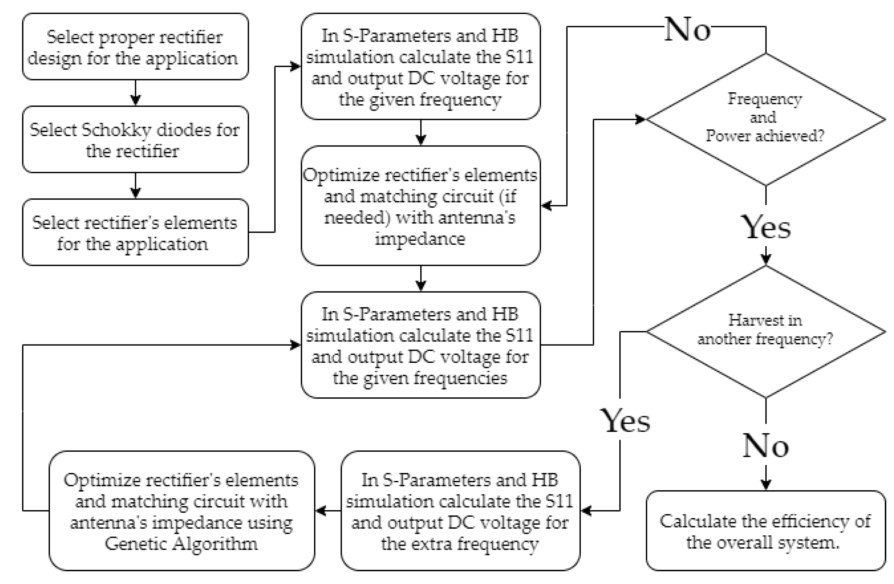
2. Radio Frequency Energy-Harvesting Design
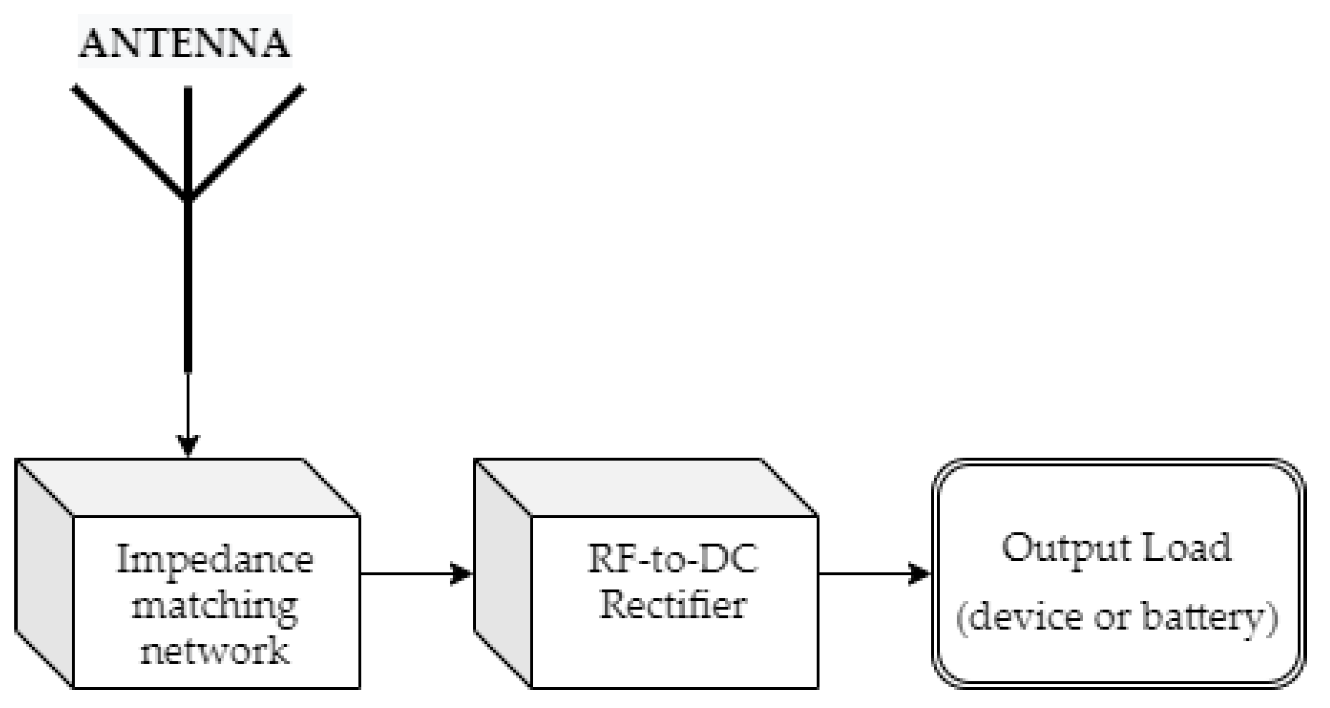
2.1. Rectenna System Design
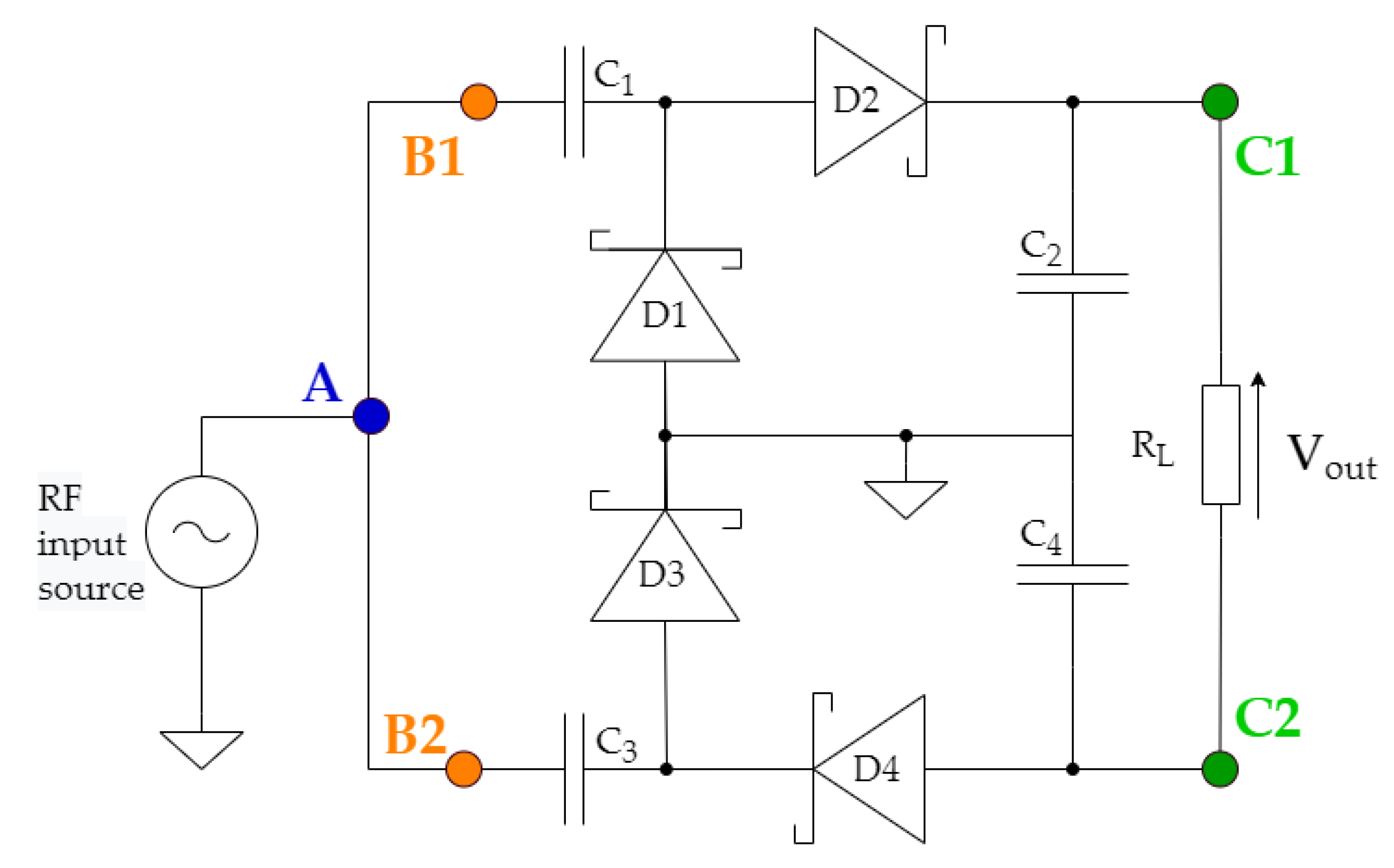
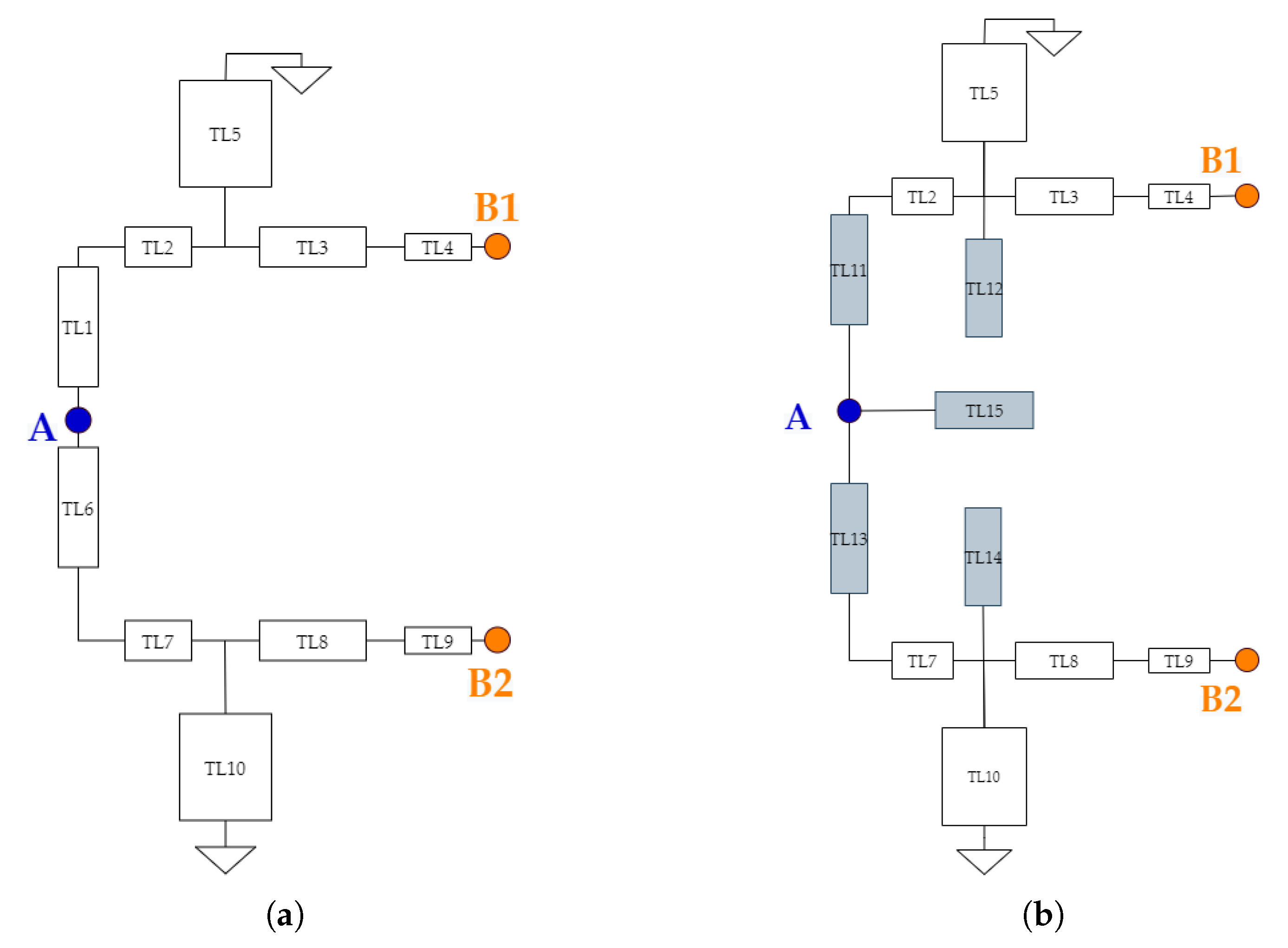
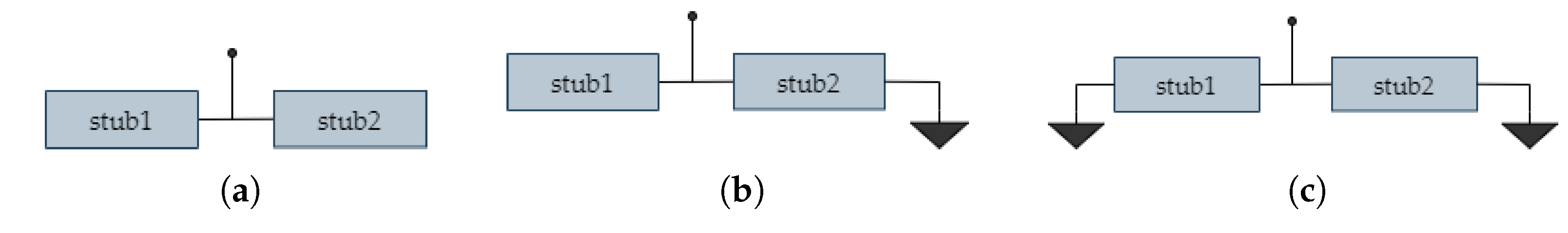
2.2. Dual-Band Rectifier Design
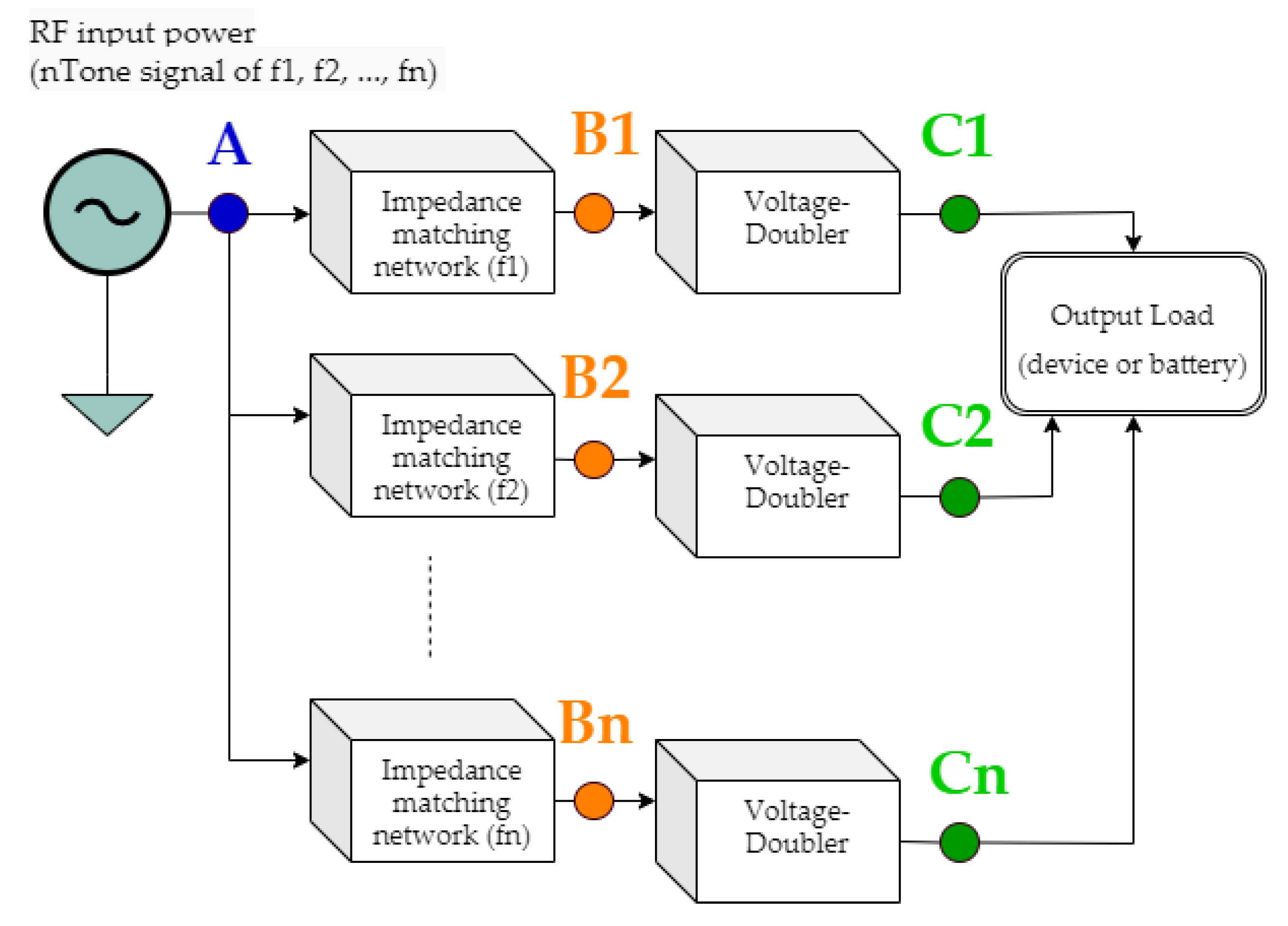
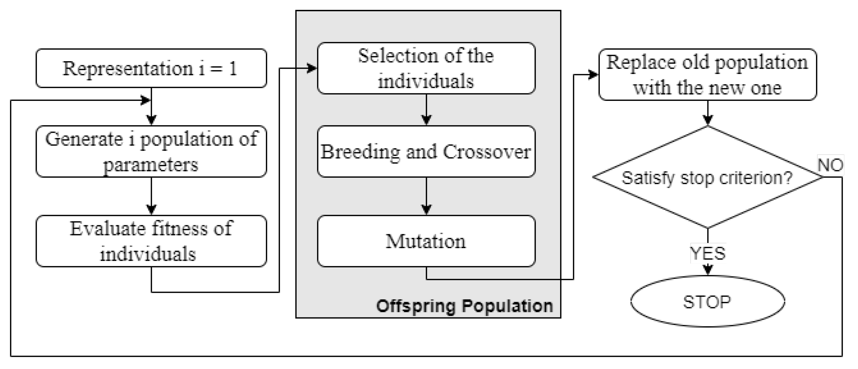
2.3. Triple-Band Rectifier Design
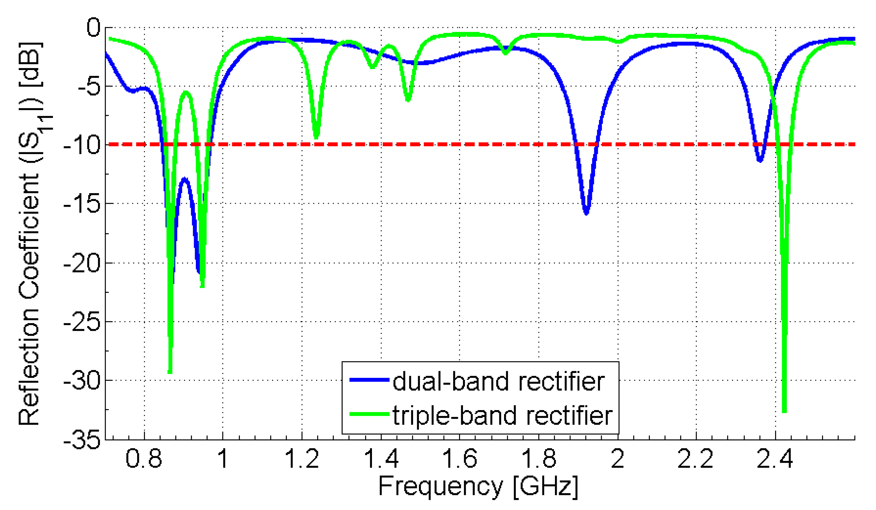
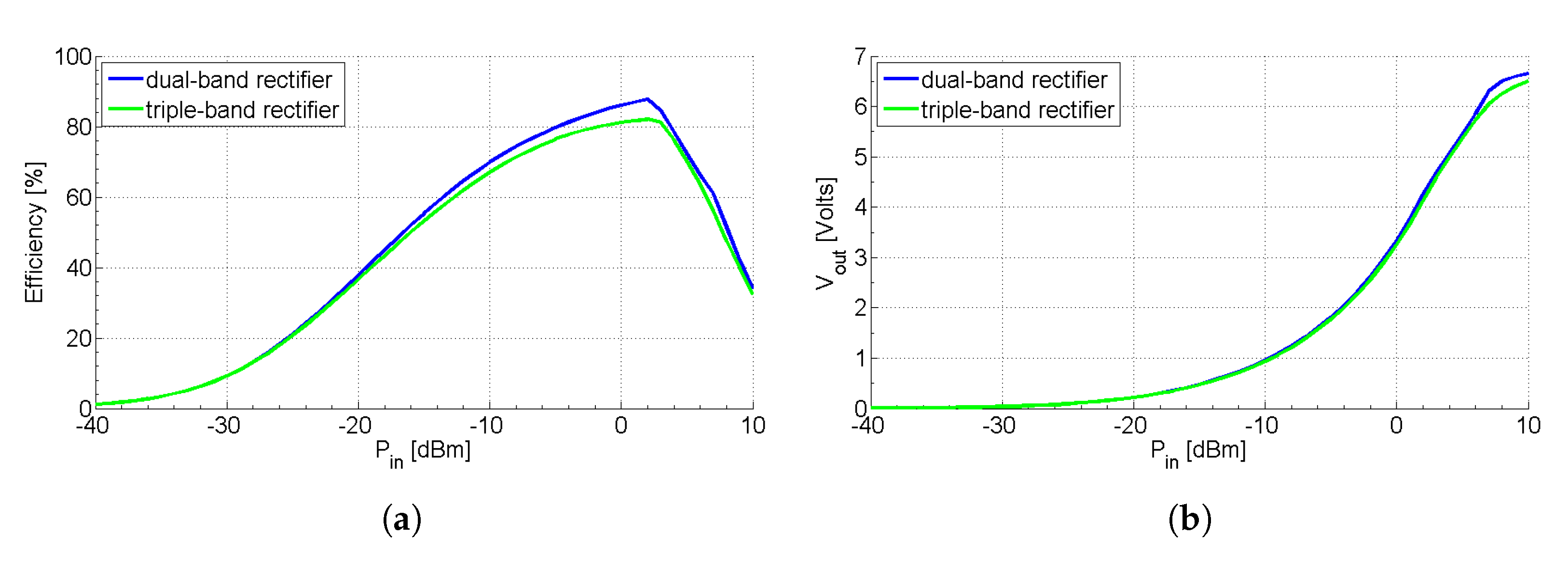
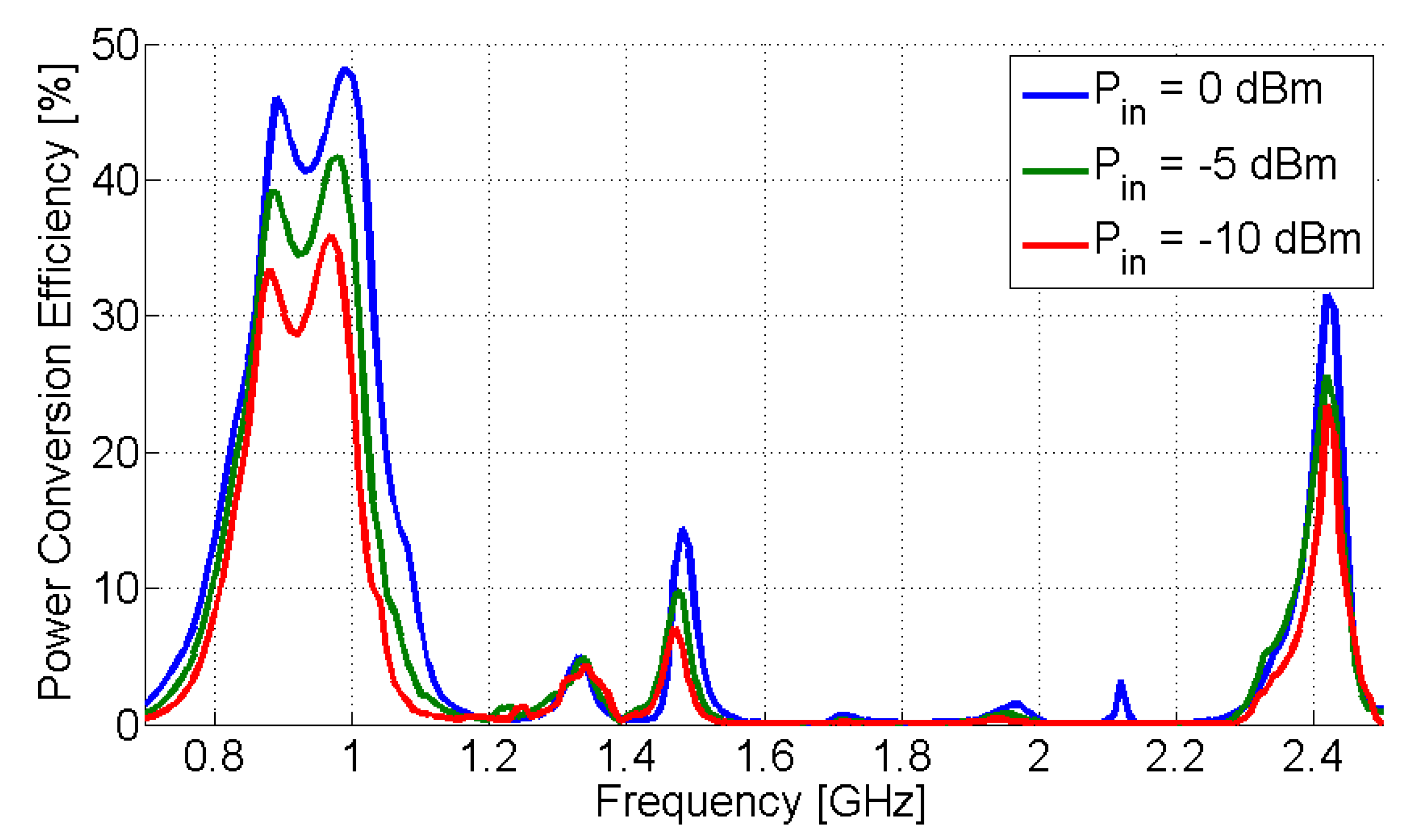
3. Results and Discussion
4. Conclusions
Author Contributions
Funding
Institutional Review Board Statement
Informed Consent Statement
Data Availability Statement
Conflicts of Interest
References
- Kim, S.; Vyas, R.; Bito, J.; Niotaki, K.; Collado, A.; Georgiadis, A.; Tentzeris, M.M. Ambient RF Energy-Harvesting Technologies for Self-Sustainable Standalone Wireless Sensor Platforms. Proc. IEEE 2014, 102, 1649–1666. [Google Scholar] [CrossRef]
- Wagih, M.; Weddell, A.S.; Beeby, S. Rectennas for Radio-Frequency Energy Harvesting and Wireless Power Transfer: A Review of Antenna Design [Antenna Applications Corner]. IEEE Antennas Propag. Mag. 2020, 62, 95–107. [Google Scholar] [CrossRef]
- Harb, A. Energy harvesting: State-of-the-art. Renew. Energy 2011, 36, 2641–2654. [Google Scholar] [CrossRef]
- Yuen, C.; Elkashlan, M.; Qian, Y.; Duong, T.Q.; Shu, L.; Schmidt, F. Energy harvesting communications: Part 1 [Guest Editorial]. IEEE Commun. Mag. 2015, 53, 68–69. [Google Scholar] [CrossRef]
- Boursianis, A.D.; Papadopoulou, M.S.; Pierezan, J.; Mariani, V.C.; Coelho, L.S.; Sarigiannidis, P.; Koulouridis, S.; Goudos, S.K. Multiband Patch Antenna Design Using Nature-Inspired Optimization Method. IEEE Open J. Antennas Propag. 2020. [Google Scholar] [CrossRef]
- Doanis, P.; Boursianis, A.; Huillery, J.; Bréard, A.; Duroc, Y.; Goudos, S. Differential Evolution in Waveform Design for Wireless Power Transfer. Telecom 2020, 1, 96–113. [Google Scholar] [CrossRef]
- Mishra, D.; De, S.; Jana, S.; Basagni, S.; Chowdhury, K.; Heinzelman, W. Smart RF energy harvesting communications: Challenges and opportunities. IEEE Commun. Mag. 2015, 53, 70–78. [Google Scholar] [CrossRef] [Green Version]
- Khansalee, E.; Zhao, Y.; Leelarasmee, E.; Nuanyai, K. A dualband rectifier for RF energy harvesting systems. In Proceedings of the 2014 11th International Conference on Electrical Engineering/Electronics, Computer, Telecommunications and Information Technology (ECTI-CON), Nakhon Ratchasima, Thailand, 14–17 May 2014; pp. 1–4. [Google Scholar] [CrossRef]
- Huang, X.; Wang, J.; Wu, X.; Liu, M. A dual-band rectifier for low-power Wireless Power Transmission system. In Proceedings of the 2015 Asia-Pacific Microwave Conference (APMC), Nanjing, China, 6–9 December 2015; pp. 1–3. [Google Scholar] [CrossRef]
- Tissier, J.; Latrach, M. Broadband rectenna for ambient RF energy harvesting applications. In Proceedings of the 2017 XXXIInd General Assembly and Scientific Symposium of the International Union of Radio Science (URSI GASS), Montreal, QC, Canada, 19–26 August 2017; pp. 1–3. [Google Scholar] [CrossRef]
- Aboualalaa, M.; Mansour, I.; Mansour, M.; Bedair, A.; Allam, A.; Abo-Zahhad, M.; Elsadek, H.; Yoshitomi, K.; Pokharel, R.K. Dual-band Rectenna Using Voltage Doubler Rectifier and Four-Section Matching Network. In Proceedings of the 2018 IEEE Wireless Power Transfer Conference (WPTC), Montreal, QC, Canada, 3–7 June 2018; pp. 1–4. [Google Scholar] [CrossRef]
- Huang, M.; Lin, Y.L.; Ou, J.; Zhang, X.; Lin, Q.W.; Che, W.; Xue, Q. Single- and Dual-Band RF Rectifiers with Extended Input Power Range Using Automatic Impedance Transforming. IEEE Trans. Microw. Theory Tech. 2019, 67, 1974–1984. [Google Scholar] [CrossRef]
- Papadopoulou, M.S.; Boursianis, A.D.; Goudos, S.K.; Psannis, K. Dual-Band Rectifier Design for Ambient RF Energy Harvesting. In Proceedings of the 2020 3rd World Symposium on Communication Engineering (WSCE), Thessaloniki, Greece, 9–11 October 2020; pp. 7–11. [Google Scholar] [CrossRef]
- Boursianis, A.D.; Papadopoulou, M.S.; Gotsis, A.; Wan, S.; Sarigiannidis, P.; Nikolaidis, S.; Goudos, S.K. Smart Irrigation System for Precision Agriculture—The AREThOU5A IoT Platform. IEEE Sens. J. 2020. [Google Scholar] [CrossRef]
- Sarma, S.S.; Chandravanshi, S.; Akhtar, M.J. Triple band differential rectifier for RF energy harvesting applications. In Proceedings of the 2016 Asia-Pacific Microwave Conference (APMC), New Delhi, India, 5–9 December 2016; pp. 1–4. [Google Scholar] [CrossRef]
- Shen, S.; Chiu, C.; Murch, R.D. A Dual-Port Triple-Band L-Probe Microstrip Patch Rectenna for Ambient RF Energy Harvesting. IEEE Antennas Wirel. Propag. Lett. 2017, 16, 3071–3074. [Google Scholar] [CrossRef]
- Chandravanshi, S.; Sarma, S.S.; Akhtar, M.J. Design of Triple Band Differential Rectenna for RF Energy Harvesting. IEEE Trans. Antennas Propag. 2018, 66, 2716–2726. [Google Scholar] [CrossRef]
- Liu, J.; Zhang, X.Y. Compact Triple-Band Rectifier for Ambient RF Energy Harvesting Application. IEEE Access 2018, 6, 19018–19024. [Google Scholar] [CrossRef]
- Tafekirt, H.; Pelegri-Sebastia, J.; Bouajaj, A.; Reda, B.M. A Sensitive Triple-Band Rectifier for Energy Harvesting Applications. IEEE Access 2020, 8, 73659–73664. [Google Scholar] [CrossRef]
- Shen, S.; Zhang, Y.; Chiu, C.; Murch, R. A Triple-Band High-Gain Multibeam Ambient RF Energy Harvesting System Utilizing Hybrid Combining. IEEE Trans. Ind. Electron. 2020, 67, 9215–9226. [Google Scholar] [CrossRef]
- Papadopoulou, M.S.; Boursianis, A.D.; Skoufa, A.; Volos, C.K.; Stouboulos, I.N.; Nikolaidis, S.; Goudos, S.K. Dual-Band RF-to-DC Rectifier with High Efficiency for RF Energy Harvesting Applications. In Proceedings of the 2020 9th International Conference on Modern Circuits and Systems Technologies (MOCAST), Bremen, Germany, 7–9 September 2020; pp. 1–4. [Google Scholar] [CrossRef]
- Brown, W.C. The History of Power Transmission by Radio Waves. IEEE Trans. Microw. Theory Tech. 1984, 32, 1230–1242. [Google Scholar] [CrossRef] [Green Version]
- Jabbar, H.; Song, Y.S.; Jeong, T.T. RF energy harvesting system and circuits for charging of mobile devices. IEEE Trans. Consum. Electron. 2010, 56, 247–253. [Google Scholar] [CrossRef]
- Xu, H.; Ortmanns, M. A Temperature and Process Compensated Ultralow-Voltage Rectifier in Standard Threshold CMOS for Energy-Harvesting Applications. IEEE Trans. Circuits Syst. II Express Briefs 2011, 58, 812–816. [Google Scholar] [CrossRef]
- Hameed, Z.; Moez, K. Hybrid Forward and Backward Threshold-Compensated RF-DC Power Converter for RF Energy Harvesting. IEEE J. Emerg. Sel. Top. Circuits Syst. 2014, 4, 335–343. [Google Scholar] [CrossRef]
- Broadcom Limited. HSMS-2850, Surface Mount Zero Bias Schottky Detector Diodes. Available online: https://docs.broadcom.com/doc/AV02-1377EN (accessed on 20 December 2020).
- Pavone, D.; Buonanno, A.; D’Urso, M.; Corte, F.D. Design Considerations for Radio Frequency Energy Harvesting Devices. Prog. Electromagn. Res. 2012, 45, 19–35. [Google Scholar] [CrossRef] [Green Version]
- Park, J.; Kim, Y.; Yoon, Y.J.; So, J.; Shin, J. Rectifier design using distributed Greinacher voltage multiplier for high frequency wireless power transmission. J. Electromagn. Eng. Sci. 2014, 14, 25–30. [Google Scholar] [CrossRef] [Green Version]
- Boursianis, A.D.; Papadopoulou, M.S.; Koulouridis, S.; Rocca, P.; Georgiadis, A.; Tentzeris, M.M.; Goudos, S.K. Triple-Band Single-Layer Rectenna for Outdoor RF Energy Harvesting Applications. Sensors 2021, 21, 3460. [Google Scholar] [CrossRef]
- Liu, Y.; Zhao, Y.; Liu, S.; Zhou, Y.; Chen, Y. Multi-Frequency Impedance Transformers for Frequency-Dependent Complex Loads. IEEE Trans. Microw. Theory Tech. 2013, 61, 3225–3235. [Google Scholar] [CrossRef]
- Song, C.; Huang, Y.; Carter, P.; Zhou, J.; Yuan, S.; Xu, Q.; Kod, M. A Novel Six-Band Dual CP Rectenna Using Improved Impedance Matching Technique for Ambient RF Energy Harvesting. IEEE Trans. Antennas Propag. 2016, 64, 3160–3171. [Google Scholar] [CrossRef] [Green Version]
- Weile, D.S.; Michielssen, E. Genetic algorithm optimization applied to electromagnetics: A review. IEEE Trans. Antennas Propag. 1997, 45, 343–353. [Google Scholar] [CrossRef]
- Sun, H.; Guo, Y.; He, M.; Zhong, Z. A Dual-Band Rectenna Using Broadband Yagi Antenna Array for Ambient RF Power Harvesting. IEEE Antennas Wirel. Propag. Lett. 2013, 12, 918–921. [Google Scholar] [CrossRef]
- Boaventura, A.; Collado, A.; Carvalho, N.B.; Georgiadis, A. Optimum behavior: Wireless power transmission system design through behavioral models and efficient synthesis techniques. IEEE Microw. Mag. 2013, 14, 26–35. [Google Scholar] [CrossRef]


| Parameter | Width/Length | Parameter | Width/Length |
|---|---|---|---|
| TL1 | 3/35 | TL6 | 3/35 |
| TL2 | 3/4 | TL7 | 3/6 |
| TL3 | 3/29 | TL8 | 3/17 |
| TL4 | 1/3 | TL9 | 1/13 |
| TL5 | 48/21 | TL10 | 39/24 |
| Parameter | Width/Length |
|---|---|
| TL11 | 3/39 |
| TL12 | 3/24.3 |
| TL13 | 3/25 |
| TL14 | 1/7.5 |
| TL15 | 48/18.3 |
| Rectifier’s Input Impedance (Ohm) | Frequency (MHz) | % Deviation from 50 Ohm | ||
|---|---|---|---|---|
| Real Part | Imaginary Part | |||
| without impedance matching | ||||
| 11.42 | −66.36 | 866 | 77.16 | |
| 27.1 | −65.4 | 937 | 45.8 | |
| with impedance matching | ||||
| dual-band (gradient optimizer) | 44.3 | 6.1 | 866 | 11.4 |
| 55 | 8.5 | 937 | 10 | |
| triple-band (genetic optimizer) | 53.48 | 0.44 | 866 | 6.96 |
| 48.81 | 9.66 | 948 | 2.38 | |
| 48.19 | −1.6 | 2423 | 3.62 | |
| Ref. | Impedance Matching | Schottky Diode | Efficiency @ Frequency | Input Power (dBm) | Load (kOhm) |
|---|---|---|---|---|---|
| [8] * | multistub | HSMS285C | 24% @ 2.1 GHz 18% @ 2.45 GHz | 10.0 | 1.60 |
| [9] * | cross- and T-shaped stubs | HSMS2850 | 57.60% @ 2.45 GHz 33.62% @ 5.8 GHz 30% @ 2.45 GHz 28% @ 5.8 GHz | 0.0 10.0 | 2.00 |
| [10] | broadband matching network | HSMS285X | ∼68% @ 975 MHz ∼55% @ 1.9 GHz | −10.0 | 15.00 |
| [11] | open and shorted stubs | HSMS2850 | 63% @ 1.95 GHz 69% @ 2.5 GHz | 7.0 3.5 | 1.00 |
| [12] * | /4 T-junction and shorted stubs | HSMS2822, HSMS2852 | 66% @ 915 MHz 58% @ 2.45 GHz | ∼30.0 ∼31.0 | 0.62 4.70 |
| [13] | microstrip line-based | HSMS2852, HSMS285C | 56.11% @ 2.67 GHz 57.95% @ 3.591 GHz | 6.0 | 2.00 |
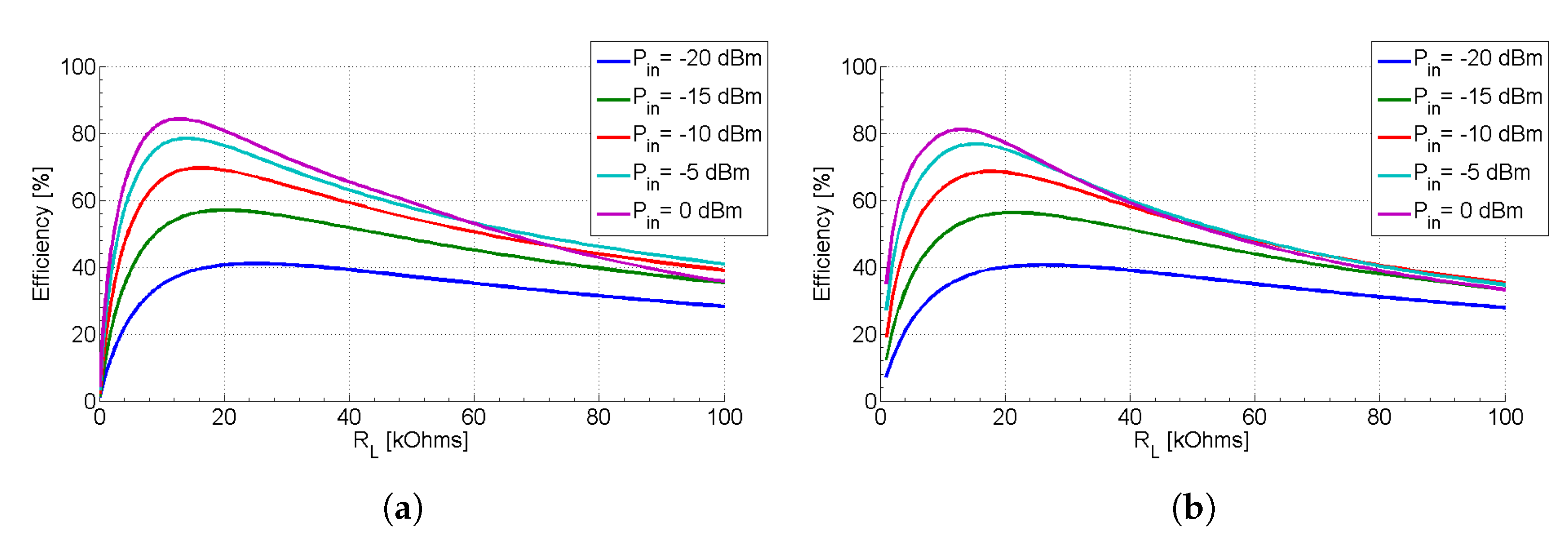
| this work | shunted stubs | HSMS285C | 48% @ 866 MHz 65% @ 940 MHz | 2.0 | 13.00 |
| Ref. | Sub. | Impedance Matching | Efficiency @ Frequency | Input Power (dBm) | Load (kOhm) |
|---|---|---|---|---|---|
| [15] | FR-4 | microstrip lines | 42% @ 3-tone signal 1.95 GHz | 10.0 | 3.00 |
| [16] * | Duroid 5880 | triple-stub, tuning and inductor | ∼41% @ 925 MHz ∼32% @ 1.82 GHz ∼26% @ 2.17 GHz | −10.0 | 5.00 |
| [17] | FR-4 | meander line, open and radial stubs | 68% @ 3-tone signal 2.0 GHz 2.47 GHz 3.6 GHz | −7.0 | 1.10 |
| [18] | Duroid 5880 | open and shorted stubs | 61.9% @ 0.85 GHz 71.5% @ 1.77 GHz 60.5% @ 2.07 GHz | 0.0 | 2.20 |
| [19] * | FR-4 | radial and shorted stubs | 54% @ 0.9 GHz 51% @ 1.8 GHz 48% @ 2.45 GHz | 4.0 | 3.80 |
| [20] * | Duroid 5880 | open and shorted stubs | ∼42% @ 1.85 GHz ∼45% @ 2.15 GHz ∼38% @ 2.48 GHz ∼48% @ 3-tone signal | −10.0 | 5.00 |
| this work | FR-4 | shunted stubs | 58% @ 866 MHz 68% @ 948 MHz 47% @ 2.423 GHz 81% @ 3-tone signal | 0.0 | 13.00 |
Publisher’s Note: MDPI stays neutral with regard to jurisdictional claims in published maps and institutional affiliations. |
© 2021 by the authors. Licensee MDPI, Basel, Switzerland. This article is an open access article distributed under the terms and conditions of the Creative Commons Attribution (CC BY) license (https://creativecommons.org/licenses/by/4.0/).
Share and Cite
Papadopoulou, M.S.; Boursianis, A.D.; Volos, C.K.; Stouboulos, I.N.; Nikolaidis, S.; Goudos, S.K. High-Efficiency Triple-Band RF-to-DC Rectifier Primary Design for RF Energy-Harvesting Systems. Telecom 2021, 2, 271-284. https://doi.org/10.3390/telecom2030018
Papadopoulou MS, Boursianis AD, Volos CK, Stouboulos IN, Nikolaidis S, Goudos SK. High-Efficiency Triple-Band RF-to-DC Rectifier Primary Design for RF Energy-Harvesting Systems. Telecom. 2021; 2(3):271-284. https://doi.org/10.3390/telecom2030018
Chicago/Turabian StylePapadopoulou, Maria S., Achilles D. Boursianis, Christos K. Volos, Ioannis N. Stouboulos, Spyridon Nikolaidis, and Sotirios K. Goudos. 2021. "High-Efficiency Triple-Band RF-to-DC Rectifier Primary Design for RF Energy-Harvesting Systems" Telecom 2, no. 3: 271-284. https://doi.org/10.3390/telecom2030018
APA StylePapadopoulou, M. S., Boursianis, A. D., Volos, C. K., Stouboulos, I. N., Nikolaidis, S., & Goudos, S. K. (2021). High-Efficiency Triple-Band RF-to-DC Rectifier Primary Design for RF Energy-Harvesting Systems. Telecom, 2(3), 271-284. https://doi.org/10.3390/telecom2030018