Article

High-Efficiency Triple-Band RF-to-DC Rectifier Primary Design for RF Energy-Harvesting Systems

by
Maria S. Papadopoulou
*,†,
Achilles D. Boursianis
*,†,
Christos K. Volos
,
Ioannis N. Stouboulos
,
Spyridon Nikolaidis
and
Sotirios K. Goudos
School of Physics, Aristotle University of Thessaloniki, 54124 Thessaloniki, Greece
*
Authors to whom correspondence should be addressed.
These authors contributed equally to this work.
Telecom 2021, 2(3), 271-284; https://doi.org/10.3390/telecom2030018
Submission received: 4 January 2021 / Revised: 19 June 2021 / Accepted: 6 August 2021 / Published: 9 August 2021
(This article belongs to the Special Issue Modern Circuits and Systems Technologies on Communications 2020)

Abstract

:
Radio Frequency (RF) energy harvesting has been emerged as a potentially reliable method to replace the costly and difficult to maintain source of low-power wireless sensor networks. A plethora of dual-band rectifier designs has been proposed in the literature operating in various frequency bands. In this paper, a triple-band RF-to-DC rectifier that operates in the frequency bands of LoRaWAN, GSM-900, and WiFi 2.4 GHz is presented. The system is composed of an impedance-matching circuit, an RF-to-DC rectifier, that converts the ambient RF energy into DC voltage able to feed low-power devices, and an output load. The proposed system resonates at three different frequencies of 866 MHz, 948 MHz and 2423 MHz, which fall within the aforementioned frequency bands of interest. The feasible solution of the proposed system was based on a dual-band rectifier operating in the frequency bands of LoRaWAN and GSM-900. A series of shunt stubs was utilized in the initial design to form the feasible solution of the proposed system. The proposed triple-band rectifier was optimized using a powerful optimization algorithm, i.e., the genetic algorithm. The overall system exhibited improved characteristics compared to the initial design in terms of its resonance. Numerical results demonstrated that the overall system exhibited an efficiency of 81% with 3.23 V of the output voltage, for an input power of 0 dBm and a load of 13 kOhm.

1. Introduction

Ambient RF sources in an urban environment are mostly incident sources such as TV/radio broadcast stations, mobile base stations, and handheld stations [1]. Ambient Electromagnetic (EM) energy harvesting has emerged as a potentially reliable method to replace the costly and quite difficult to maintain source of wireless sensor networks [2,3]. Unlike other harvesting techniques that are strongly dependent on exogenous factors, such as climate or environmental conditions, RF energy harvesting and Wireless Power Transfer (WPT) are mostly related to the radio propagation channel [1,4,5,6], so it is better suited to supporting Quality-of-Service (QoS)-based applications [7].
Recently, a plethora of dual-band rectifier designs has been proposed in the literature. In 2014 [8], an RF rectifier for energy harvesting applications that operated at 2.10 GHz and 2.45 GHz was presented. The system was comprised of a multistub impedance-matching network, a Schottky diode, and a DC pass filter. The authors reported that their proposed rectifier achieved an efficiency of 24% and 18% at 2.10 GHz and 2.45 GHz, respectively, for an input power of 10 dBm and a load impedance of 1.6 kOhm. In 2015 [9], a rectifier that resonated at 2.45 GHz and 5.8 GHz was presented. The rectifier consisted of a matching circuit, a Schottky HSMS2850 diode, a DC pass filter, and a load. The authors achieved an efficiency of 57.6% and 33.6% for an input power of 0 dBm and 30% and 28% for an input power of 10 dBm, at 2.45 GHz and 5.80 GHz, respectively. In 2017 [10], Tissier et al. introduced a dual-band rectifier in the GSM-900 and GSM-1800 bands. The rectifier topology was based on a Latour doubler. The efficiency obtained was greater than 30% at 942 MHz and greater than 20% at 1805 MHz for an input power greater than −10 dBm and an output load equal to 15 kOhm. In 2018 [11], a voltage-doubler circuit as a rectifier was introduced, which consisted of two Avago HSMS2850 Schottky diodes and two capacitors. The results demonstrated that the RF-to-DC maximum efficiency was 63% at 1.95 GHz and 69% at 2.50 GHz, for an input power of 7.0 dBm and 3.5 dBm, respectively, and a resistive load of 1.0 kOhm. In 2019, Huang et al. [12] utilized a λ /4 T-junction power divider to connect two branches of a rectifier, to extend the range of input power of the system with high conversion efficiency. They applied their proposed technique to both single- and dual-band rectifiers. They reported a measured peak efficiency of 68% for the single-band rectifier (915 MHz) and an input power range from −5 dBm to 31 dBm by setting an efficiency threshold of more than 70% of its peak efficiency of 66% for an input power range from −6 dBm to 33 dBm (efficiency threshold greater than 70%) at 915 MHz and a peak efficiency of 58% for an input power range from 10 dBm to 32 dBm (efficiency threshold greater than 70%) at 2.45 GHz. In 2020 [13], a system was proposed that resonated in the frequency bands of 4G (2.67 GHz) and 5G (3.591 GHz) mobile communication systems. Numerical results demonstrated that the RF-to-DC maximum efficiency was 56.11% at 2.67 GHz and 57.95% at 3.591 GHz, for an input power of 6.0 dBm and a resistive load of 2.0 kOhm. The same year, Boursianis et al. [14] introduced a rectenna system for precision agriculture. The two-stage rectifier circuit was based on the Greinacher voltage-doubler and operated in the LoRaWAN (863 MHz–870 MHz) and EGSM-900 (925 MHz–960 MHz) mobile communication frequency bands. The maximum simulated and measured efficiency of 75% and 73.6% were achieved for input power P i n = 2 dBm and 4.8 dBm, respectively, for an output load equal to 7 kOhm.
The ever-increasing demand for more energy, as well as the remarkable augmentation of ambient RF energy sources led the scientific community to consider triple-band rectifiers as an efficient technique to harvest even more power. In 2016 [15], a triple-band differential rectifier using a single-stage Villard topology was designed. They used microstrip lines to implement an impedance-matching network and achieved a maximum efficiency of 42% for an input power of 14 dBm. In 2017 [16], a triple-band rectifier operating at 925 MHz (GSM-900), 1820 MHz (GSM-1800), and 2170 MHz (UMTS), respectively, was proposed. Numerical results indicated that the peak efficiency was 41%, 32%, and 26% for an input power of −10 dBm and for the three aforementioned bands, respectively. In 2018, Chandravanshi et al. [17] designed a triple-band rectifier with an impedance-matching network comprised of meander lines and open- and radial-stubs. A peak efficiency of 68% was achieved for a three-tone signal and input power of −7 dBm, whereas the output load was equal to 1.1 kOhm. The same year, Liu et al. [18] introduced a rectifier design with a triple-band impedance-matching network. The system resonated at 0.85 GHz, 1.77 GHz, and 2.07 GHz, whereas the well-known Schottky diode HSMS2850 from Avago Technologies was selected due to its low biasing voltage. They achieved maximum efficiencies of 61.9%, 71.5%, and 60.5% at the three frequencies of interest. In 2020 [19], the authors presented a triple-band system that simultaneously harvested ambient RF energy at relatively low and medium input power densities. For an input power level of −10 dBm, they achieved a power conversion efficiency of 33.7%, 21.8%, and 20% at 0.9 GHz, 1.8 GHz, and 2.45 GHz, respectively. For an input power of 4 dBm, a maximum efficiency of 54%, 51%, and 48% was achieved for the above frequencies. Finally, the same year, Shen et al. [20], to overcome the challenge of battery recharging and/or replacement in industry, proposed a triple-band high-gain multibeam ambient RF-to-DC rectifier for the GSM-1800, UMTS-2100, and WiFi 2.4 GHz frequency bands. They managed a maximum power conversion efficiency of 42%, 45%, and 38% for an input power of −10 dBm and an output load of 5.0 kOhm at 1.85 GHz, 2.15 GHz, and 2.48 GHz, respectively.
In this work, a novel triple-band rectifier that operates in the frequency bands of the LoRaWAN network, the GSM-900 mobile communication network, and the WiFi 2.4 GHz wireless network is presented. It is an extended version of the work presented in [21]. The RF-to-DC rectifier resonates at three different frequencies, i.e., 866 MHz, 948 MHz, and 2.423 GHz, which fall into the previously mentioned frequency bands. For the rectification unit, a single-layer voltage-doubler circuit was utilized that operates in the previously mentioned frequencies. A series of shunt stubs was applied to the initial design of the RF-to-DC rectifier to form the proposed triple-band system. A feasible solution of the proposed system was obtained by the utilization of a powerful genetic algorithm optimizer.
The remainder of the paper is as follows. In Section 2, a detailed description of the proposed radio frequency energy-harvesting system is presented, indicating the Schottky diode-based dual- and triple-band rectifying circuits. Section 3 summarizes the main results of the proposed rectifier and evaluates its performance. Finally, Section 4 concludes with the findings of the paper.

2. Radio Frequency Energy-Harvesting Design

2.1. Rectenna System Design

The rectifying antenna (rectenna) is a joint system of an antenna and an RF-to-DC rectifier. The antenna is responsible for capturing the ambient RF electromagnetic energy, whereas the rectifier converts the input AC voltage into DC voltage, able to feed low-power electronic devices. In many cases, an impedance-matching network intervenes between the RF-to-DC rectifier and the antenna, to adjust the impedance between these two elements. Brown [22] invented the first rectenna in the early 1960s. Since then, the technological revolution has encouraged researchers to design and fabricate more efficient and sophisticated circuits. Figure 1 illustrates the basic block diagram of a rectenna system.

2.2. Dual-Band Rectifier Design

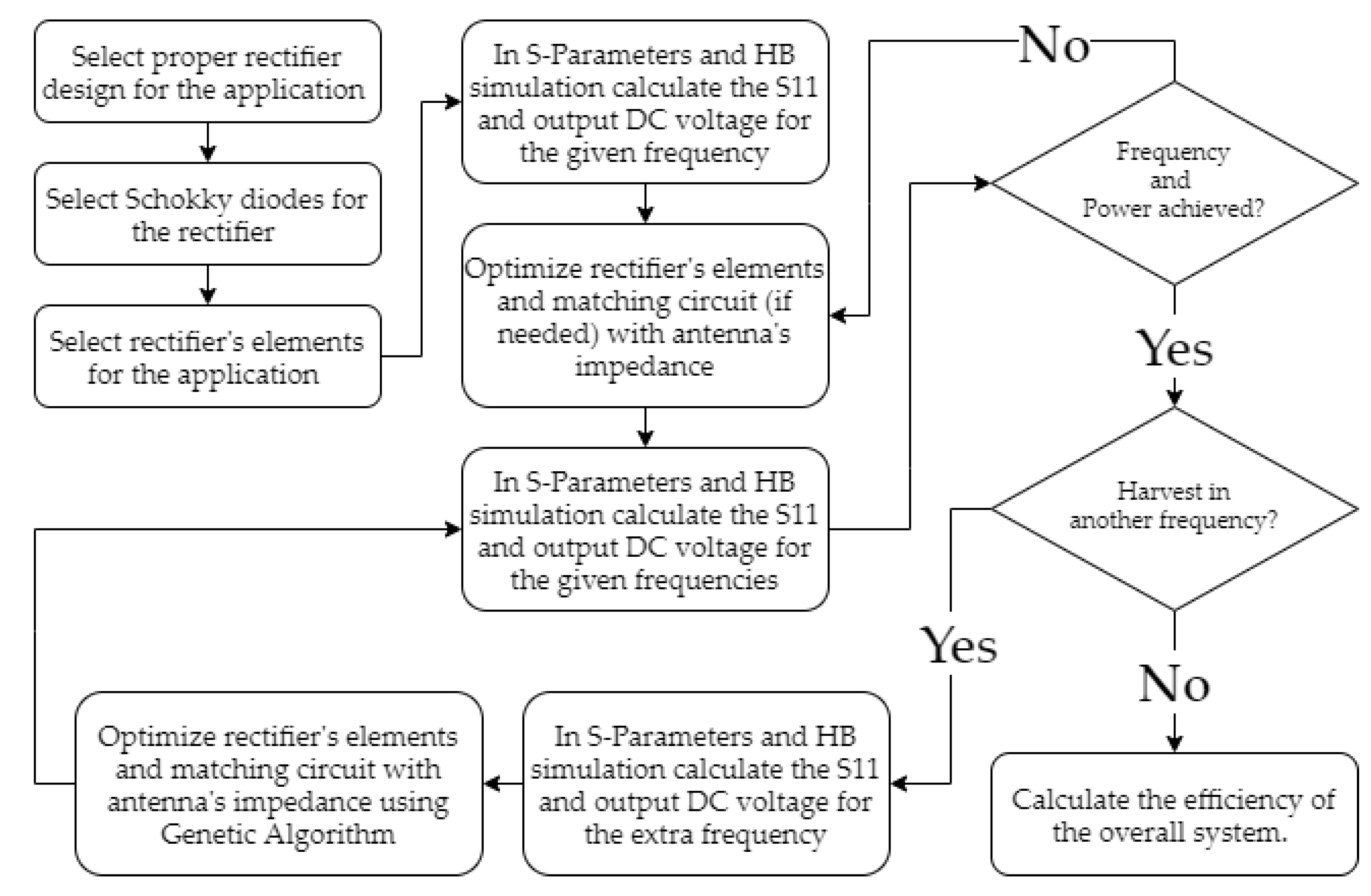
The rectifier circuit is at the heart of an energy-harvesting module. It is responsible for converting the received RF power into DC voltage, sufficiently enough to charge a battery or feed battery-free low-power electronics. It is decisive in providing high values of RF-to-DC power conversion efficiency and operating in multifrequency bands to convert as much ambient RF energy as possible. One of the most established approaches to design an RF-to-DC rectifier is the Schottky diode-based rectifying circuit [23]. Figure 2 illustrates the design process of the proposed Schottky diode-based rectifier, as well as the main considerations that are taken into account. Based on Figure 2, the first steps of a rectifier’s design were to select the appropriate circuit type and elements (Schottky diodes, resistors, capacitors). The Schottky diode, to which is attributed a low forward voltage drop and low substrate leakage, can improve the RF-to-DC conversion efficiency, as well as the DC output voltage [24,25]. Thereinafter, we calculated the S-parameters, the power conversion efficiency (PCE), and the DC output voltage of the system using the Advanced Design System (ADS-© Keysight Technologies 2000–2021). The variations of the rectifier’s input impedance with the RF input power resulted in the use of the Large-Signal S-Parameter simulation tool of ADS. Depending on the outcomes, the next steps involved the tuning of the physical parameters of the impedance-matching network to adjust to a standard antenna port of 50 Ohm and the recalculation of the previously mentioned parameters. We repeated the same procedure for every frequency of interest until we met the desired criteria. Finally, we computed the efficiency and DC output voltage of the overall circuit as a function of the incident RF input signal.
In this work, the HSMS285C (SOT-323) Schottky barrier diode, which has a low forward voltage value of V F = 150 mV, was utilized [26]. The generalized configuration approach of the utilized rectifier is illustrated in Figure 3. Two different impedance-matching circuits were designed to interconnect the antenna module with the branches of the rectifier [21]. The system was designed using the Harmonic Balance (HB) method in the Advanced Design System software (ADS-© Keysight Technologies 2000–2021). An FR-4 substrate (dielectric constant ( ϵ r ) = 4.4, substrate thickness = 1.6 mm, dielectric loss tangent ( t a n δ ) = 0.02, and copper thickness = 0.07 mm) was applied for the design of the utilized system. Furthermore, the Greinacher voltage-doubler topology was selected due to its higher output DC voltage against other alternative topologies for a given input power level [27]. Moreover, Park et al. [28] reported that the Greinacher voltage multiplier can be employed in high-power WPT systems, while Boursianis et al. [29] presented an output DC voltage over 420 mV for an input power equal to −10 dBm. In some cases, if we consider low-power values at the input of the rectifier, single-diode topologies may outperform voltage-doubler topologies. However, the single-diode topology was not considered in this work, due to the comparative DC output voltage characteristic of the Greinacher topology.
Figure 4 portrays the configuration of the Greinacher voltage-doubler that was utilized in the presented rectifier [21]. The voltage-doubler uses 2 zero-bias Schottky surface-mounted Avago HSMS285C series diodes and 2 capacitors C 1 = C 2 = 100 pF (AVX 08053K) with 1% tolerance. The rest of the voltage-doubler components are several conductor lines of the appropriate width (W) and length (L) to ensure a compact layout design. The input RF AC signal was rectified by the voltage-doubler circuit. The latter was comprised of a voltage clamp (diode D 1 and capacitor C 1 ) and a peak rectifier (diode D 2 and capacitor C 2 ).
To ensure that maximum power conversion efficiency and maximum sensitivity will be achieved, an impedance-matching network should be utilized. We considered a standard antenna port of Z A = 50 Ohm. The overall system performance can be evaluated by the RF-to-DC power conversion efficiency versus the incident RF signal ( P i n ) at the input port A. Figure 5a illustrates the geometry of the proposed impedance-matching circuit for the corresponding operating frequencies of the dual-band rectifying circuit, whereas Table 1 presents the optimal physical parameters of the transmission lines obtained by the S-parameter simulation controller toolbox (ADS-© Keysight Technologies 2000–2021), which is based on the Gradient optimizer.

2.3. Triple-Band Rectifier Design

Liu et al. [30] realized dual- and triple-band circuits by using one or more parallel shunt stubs. They proved that when impedance matching is required on more than one frequency bands, more circuit freedoms are necessary for the design. They obtained the extra triple- and quad-frequency bands from a dual-band design by applying a parallel combination of two stubs to provide the needed susceptances. Figure 6 illustrates the three basic topologies of two shunt combinations, open-open (Figure 6a), open-shorted (Figure 6b), and shorted-shorted (Figure 6c). Furthermore, Song et al. [31] designed a six-band rectifier with only three voltage-doubler circuits connected in series. The presented system had an excellent performance in various conditions, such as multiple frequency bands and a wide range of input power levels.
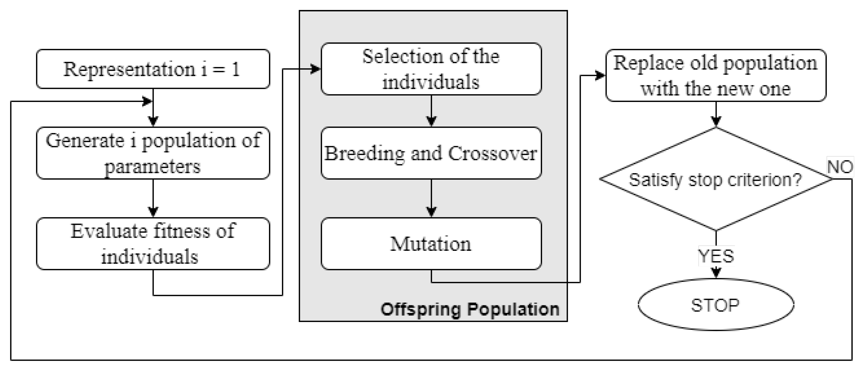
The main idea of the proposed design is to add a tuning frequency to the dual-band impedance-matching network illustrated in Figure 5a without increasing the complexity of the derived triple-band system by adding an extra branch. Therefore, we proposed the triple-band impedance-matching network topology of Figure 5b, where a combination of shunt stubs is introduced to achieve the third resonating frequency. To design the triple-band rectifier, we utilized the genetic optimizer in the Advanced Design System software (ADS-© Keysight Technologies 2000–2021) by obtaining a feasible solution of the corresponding parameters, including the sizes (length, width) of the shunt stubs. It is worth mentioning that there is no unique winning strategy for the optimization due to the complexity of the system design. The application of these optimization techniques requires many tuning parameters. Genetic optimization techniques have proven to be effective for many complex optimization problems. The Genetic Algorithm (GA) optimization method is a procedure where a set of parameters, the chromosomes, can evolve to a new set of parameters [32]. The basic idea is that with each change in the parameter population, the performance improves, so the survival of the fittest is achieved. It is a five-step process: (1) representation, (2) evaluation, (3) reproduction, (4) breeding and crossover, and (5) mutation. Figure 7 demonstrates the genetic optimization algorithm. Having the previous dual-band design as a starting point, we applied the shunt stubs technique along with the genetic algorithm optimizer to obtain a feasible geometry for the impedance-matching network of the triple-band rectifier (Figure 5b). The stopping criterion was set to 1000 iterations, whereas the average computational time for each iteration was about 3 min. Table 2 lists the optimized physical parameters of the transmission lines for the triple-band rectifier design of Figure 5b.

3. Results and Discussion

The voltage-doubler input impedance for the dual-band design was computed using the S-parameters simulator of the Advanced Design System (ADS) software. The derived values before the impedance matching were 11.42 j 66.36 and 27.1 j 65.4 at 866 MHz and 937 MHz, respectively. We considered a standard antenna port of 50 Ohm. The size of the impedance-matching circuits was optimized and adjusted to the input impedance of the overall system. The derived values after the impedance matching were 44.3 + j 6.1 and 55.0 + j 8.5 at the two frequencies of interest. To obtain the impedance matching of the overall system, a simple short-circuited stub was included, as depicted in Figure 5b. Additionally, the input impedance for the triple-band design was computed, and the derived values were 53.48 + j 0.44 , 48.81 + j 9.66 , and 48.19 j 1.6 at 866 MHz, 948 MHz, and 2.423 GHz, respectively. Table 3 lists the previously mentioned input impedance values of the dual- and triple-band rectifier, with and without the impedance-matching network, at the frequencies of interest. We can derive that the percent deviation of the input impedance of the dual-band rectifying circuit, calculated using the gradient optimizer, was greater than 10%. Simultaneously, the percent deviation of the computed input impedance using genetic algorithm optimizer for the triple-band rectifying circuit was less than 7%.
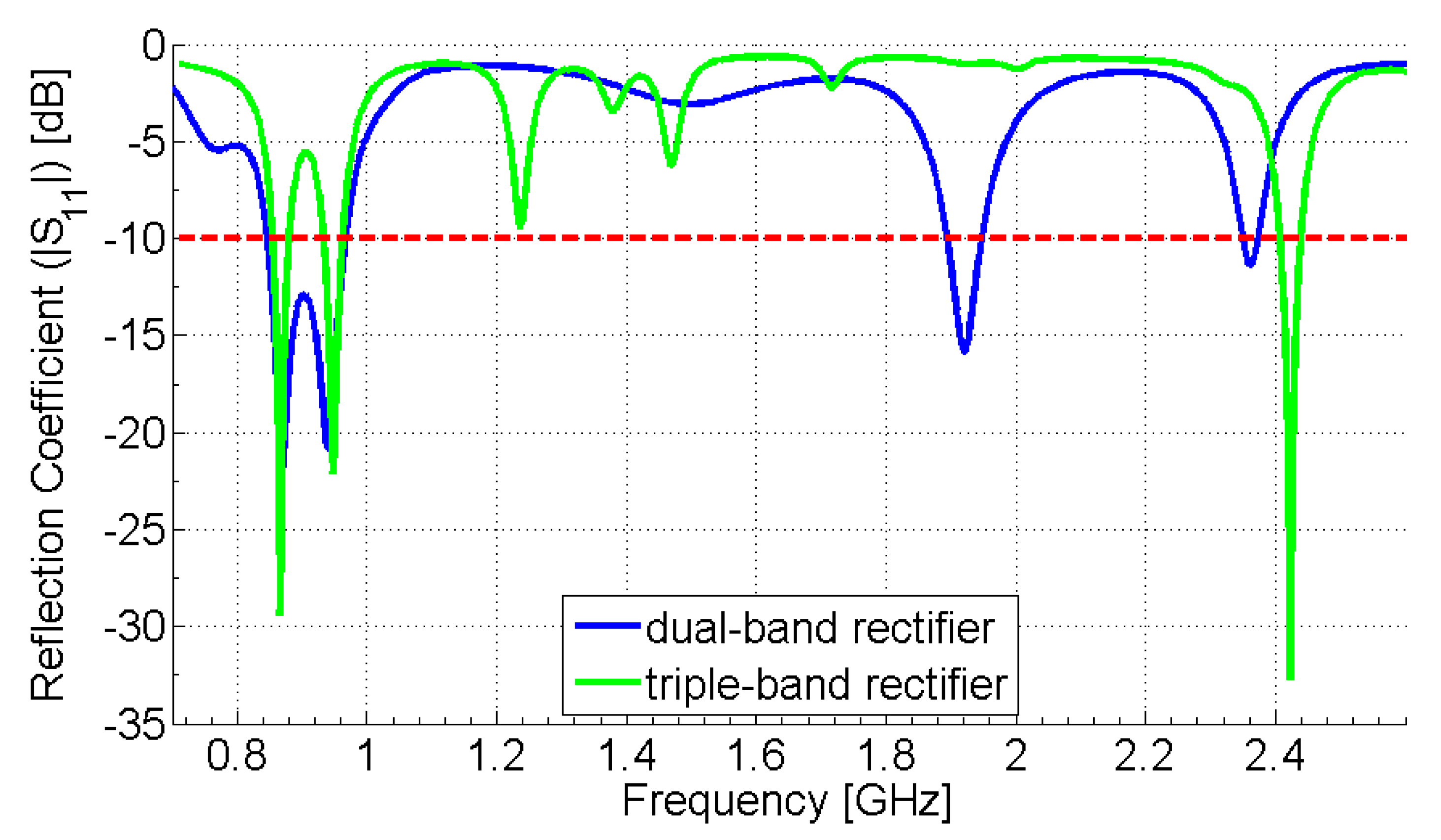
Figure 8 illustrates the S11 magnitude (reflection coefficient) of the proposed dual- and triple-band RF-to-DC rectifier versus frequency. From the presented graph, we can derive that the dual-band rectifying circuit operates satisfactorily in the European LoRaWAN frequency band (863–870 MHz), as well as in the GSM-900 mobile communication frequency band (880–960 MHz). The utilized rectifier has a dual-frequency operation (−21.89 dB at 869 MHz and −20.87 dB at 940 MHz) that falls into the previously mentioned frequency bands. It is also noteworthy that the −10 dB bandwidth of the proposed rectifier extends to 121 MHz (846–967 MHz).
Furthermore, we can observe that the triple-band rectifying circuit operates satisfactorily in the European LoRaWAN frequency band (863–870 MHz), the GSM-900 (880–960 MHz) mobile communication frequency band, and the WiFi 2.4 GHz wireless network frequency band. The proposed rectifier has a triple-frequency operation (−29.4 dB at 866 MHz, −22.13 dB at 948 MHz, and −32.75 dB at 2.423 GHz) within the previously mentioned frequency bands. The −10 dB bandwidth of the proposed rectifier in the three distinguished regions is 27 MHz (853–880 MHz), 29 MHz (933–962 MHz), and 33 MHz (2.406–2.439 GHz), respectively. We should also point out that, besides the third tuning operation achieved by the shunt stubs method along with the GA optimizer, the tuning operation in the first two frequency bands was improved by 7.51 dB and 1.96 dB, respectively.
The overall system RF-to-DC efficiency n is computed as follows:
n = P D C P i n
P D C = V o u t 2 R L
where P D C is the total output DC power, calculated by the sum of each RF power P D C , f 1 , P D C , f 2 , and P D C , f 3 corresponding to an RF input power at a frequency of f 1 = 866 MHz, f 2 = 948 MHz, and f 3 = 2423 MHz, respectively, P i n is the RF input power, V o u t is the output DC voltage, and R L is the load resistance. We should point out that for an input signal of two (dual-band rectifier) or three tones (triple-band rectifier), the total power of the two or three tones is counted as the input power P i n , respectively [33].
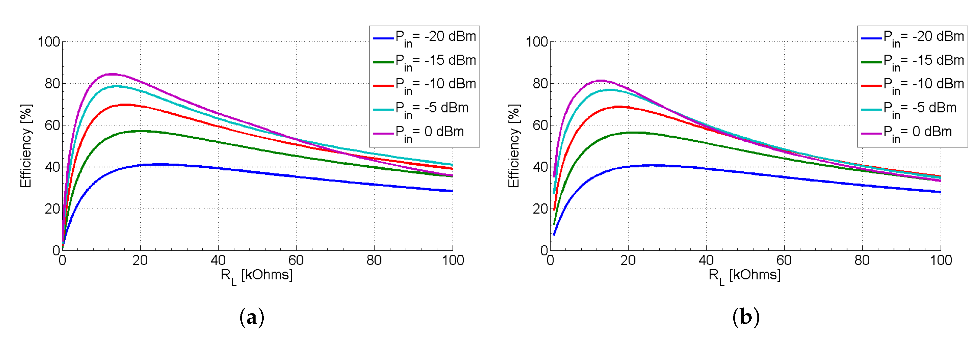
Figure Figure 9 displays the RF-to-DC efficiency versus the R L output load of the dual-band (Figure 9a: two-tone signal) and triple-band (Figure 9b: three-tone signal) rectifying circuit.
From the presented curves of the graph, we can easily derive that the maximum efficiency of the proposed dual-band rectifier for an input power of 2 dBm is 85.9%, whereas the optimum output load is equal to 13 kOhm. At −20 dBm, −15 dBm, −10 dBm, and −5 dBm, the obtained conversion efficiencies are 38%, 55%, 69%, and 78%, respectively. For the triple-band rectifier, the maximum power conversion efficiency is 81.9%. Additionally, at −20 dBm, −15 dBm, −10 dBm, and −5 dBm, the obtained conversion efficiencies for an output load of 13 kOhm are 36%, 53%, 67%, and 76%. Therefore, we can conclude that the given topology of the rectifier design has the features of stability and durability if we consider the efficiency values at different input power values.
Finally, Figure 10a,b portrays the RF-to-DC efficiency and the DC output voltage V o u t versus the RF input power P i n , respectively. From Figure 10a, we can observe that the efficiency of the dual-band rectifier is 85% for an input power level of 0 dBm (two-tone signal), whereas in the triple-band system, it is 81% (three-tone signal). For an input power equal to 2 dBm, the maximum power conversion efficiency of the dual- and triple-band circuits is 85.9% and 81.9%, respectively. One may notice that there is a reduction in the PCE of the triple-band system compared to the PCE of the dual-band system; however, this variation is indiscernible. From the results of Figure 10b, we can conclude that the DC output voltage for an RF input power level greater than −15 dBm is above 0.5 V, whereas for an input power of 0 dBm, it is 3.32 V and 3.24 V for the dual- and triple-band rectifier, respectively. Additionally, Figure 11 illustrates the RF-to-DC efficiency versus frequency for various input power levels P i n . From the presented curves, we can verify the system’s performance in the frequency bands of interest.
Table 4 lists the comparative results of this work against previous studies that were based on dual-band rectifiers. It is noteworthy that, among the designs, the proposed system exhibits quite satisfactory performance, and it is one of the three circuits that displays the maximum conversion efficiency for an input power signal below 6 dBm (about 4.0 mW). Furthermore, the maximum power conversion efficiency of the dual-band proposed rectifier in a two-tone signal (concurrent) is 85.9% for an input power of 2 dBm and a load of 13 kOhm.
Table 5 lists the comparative results of this work against previous studies that were based on triple-band rectifiers. It is noteworthy that, among the designs with the low-cost substrate of FR-4, the proposed system exhibits quite satisfactory performance. Furthermore, it is one of the designs that achieves the maximum conversion efficiency for an input power signal below 4 dBm (about 2.5 mW). Furthermore, the maximum power conversion efficiency of the triple-band proposed rectifier in a three-tone signal (concurrent) is 81.9% for an input power of 2 dBm and an output load of 13 kOhm. This result surpasses the rest of the circuits described in the studies that are included in Table 4.

4. Conclusions

In this work, a Schottky diode-based triple-band rectifier was proposed. The feasible solution of the proposed system was based on an initial design of a dual-band rectifier. It consisted of an impedance-matching circuit, an RF-to-DC rectifier that converts ambient RF energy into DC voltage, and an output load. A series of shunt stubs was applied to the initial design of the dual-band rectifier to form the proposed system. The transmission lines of the triple-band rectifier were optimized by utilizing a genetic algorithm optimizer. The obtained feasible solution of the proposed system operated satisfactorily in the frequency bands of LoRaWAN networks, GSM-900 mobile communication networks, and WiFi 2.4 GHz wireless networks. The numerical results of the proposed system exhibited a triple-frequency operation (−29.4 dB at 866 MHz, −22.13 dB at 948 MHz, and −32.75 dB at 2.423 GHz), whereas the power conversion efficiency reached up to 81% for an input power level of 0 dBm. It is worth mentioning that the DC output voltage for an RF input power level greater than −15 dBm was above 0.5 V, whereas for an input power of 0 dBm, was equal to 3.24 V. The presented results of the proposed triple-band rectifier demonstrate the system’s stability and durability in the frequency bands of interest. Future work includes the fabrication of the proposed system, as well as its experimental validation by combining various antenna prototypes in a rectenna system. Furthermore, knowing that, depending on the total input power of the rectifier, topologies with a reduced number of rectifying elements may lead to better RF-to-DC PCE [34], we will incorporate the above study to assess the performance of the new circuit design in our future work.

Author Contributions

The conceptualization of the paper was by M.S.P. and A.D.B.; M.S.P. performed the theoretical analysis and the simulations. A.D.B., S.N., and S.K.G. validated the theoretical analysis and the simulation results. A.D.B., S.N., and S.K.G. supervised the process. M.S.P., A.D.B., and S.K.G. analyzed the results and contributed to writing the manuscript. All authors contributed to reviewing the manuscript. All authors read and agreed to the published version of the manuscript.

Funding

This research was cofinanced by the European Union and Greek national funds through the Operational Program Competitiveness, Entrepreneurship and Innovation, under the call RESEARCH-CREATE-INNOVATE (project code: T1EDK-05274).

Institutional Review Board Statement

Not applicable.

Informed Consent Statement

Not applicable.

Data Availability Statement

No new data were created or analyzed in this study. Data sharing is not applicable to this article.

Conflicts of Interest

The authors declare no conflict of interest.

References

  1. Kim, S.; Vyas, R.; Bito, J.; Niotaki, K.; Collado, A.; Georgiadis, A.; Tentzeris, M.M. Ambient RF Energy-Harvesting Technologies for Self-Sustainable Standalone Wireless Sensor Platforms. Proc. IEEE 2014, 102, 1649–1666. [Google Scholar] [CrossRef]
  2. Wagih, M.; Weddell, A.S.; Beeby, S. Rectennas for Radio-Frequency Energy Harvesting and Wireless Power Transfer: A Review of Antenna Design [Antenna Applications Corner]. IEEE Antennas Propag. Mag. 2020, 62, 95–107. [Google Scholar] [CrossRef]
  3. Harb, A. Energy harvesting: State-of-the-art. Renew. Energy 2011, 36, 2641–2654. [Google Scholar] [CrossRef]
  4. Yuen, C.; Elkashlan, M.; Qian, Y.; Duong, T.Q.; Shu, L.; Schmidt, F. Energy harvesting communications: Part 1 [Guest Editorial]. IEEE Commun. Mag. 2015, 53, 68–69. [Google Scholar] [CrossRef]
  5. Boursianis, A.D.; Papadopoulou, M.S.; Pierezan, J.; Mariani, V.C.; Coelho, L.S.; Sarigiannidis, P.; Koulouridis, S.; Goudos, S.K. Multiband Patch Antenna Design Using Nature-Inspired Optimization Method. IEEE Open J. Antennas Propag. 2020. [Google Scholar] [CrossRef]
  6. Doanis, P.; Boursianis, A.; Huillery, J.; Bréard, A.; Duroc, Y.; Goudos, S. Differential Evolution in Waveform Design for Wireless Power Transfer. Telecom 2020, 1, 96–113. [Google Scholar] [CrossRef]
  7. Mishra, D.; De, S.; Jana, S.; Basagni, S.; Chowdhury, K.; Heinzelman, W. Smart RF energy harvesting communications: Challenges and opportunities. IEEE Commun. Mag. 2015, 53, 70–78. [Google Scholar] [CrossRef] [Green Version]
  8. Khansalee, E.; Zhao, Y.; Leelarasmee, E.; Nuanyai, K. A dualband rectifier for RF energy harvesting systems. In Proceedings of the 2014 11th International Conference on Electrical Engineering/Electronics, Computer, Telecommunications and Information Technology (ECTI-CON), Nakhon Ratchasima, Thailand, 14–17 May 2014; pp. 1–4. [Google Scholar] [CrossRef]
  9. Huang, X.; Wang, J.; Wu, X.; Liu, M. A dual-band rectifier for low-power Wireless Power Transmission system. In Proceedings of the 2015 Asia-Pacific Microwave Conference (APMC), Nanjing, China, 6–9 December 2015; pp. 1–3. [Google Scholar] [CrossRef]
  10. Tissier, J.; Latrach, M. Broadband rectenna for ambient RF energy harvesting applications. In Proceedings of the 2017 XXXIInd General Assembly and Scientific Symposium of the International Union of Radio Science (URSI GASS), Montreal, QC, Canada, 19–26 August 2017; pp. 1–3. [Google Scholar] [CrossRef]
  11. Aboualalaa, M.; Mansour, I.; Mansour, M.; Bedair, A.; Allam, A.; Abo-Zahhad, M.; Elsadek, H.; Yoshitomi, K.; Pokharel, R.K. Dual-band Rectenna Using Voltage Doubler Rectifier and Four-Section Matching Network. In Proceedings of the 2018 IEEE Wireless Power Transfer Conference (WPTC), Montreal, QC, Canada, 3–7 June 2018; pp. 1–4. [Google Scholar] [CrossRef]
  12. Huang, M.; Lin, Y.L.; Ou, J.; Zhang, X.; Lin, Q.W.; Che, W.; Xue, Q. Single- and Dual-Band RF Rectifiers with Extended Input Power Range Using Automatic Impedance Transforming. IEEE Trans. Microw. Theory Tech. 2019, 67, 1974–1984. [Google Scholar] [CrossRef]
  13. Papadopoulou, M.S.; Boursianis, A.D.; Goudos, S.K.; Psannis, K. Dual-Band Rectifier Design for Ambient RF Energy Harvesting. In Proceedings of the 2020 3rd World Symposium on Communication Engineering (WSCE), Thessaloniki, Greece, 9–11 October 2020; pp. 7–11. [Google Scholar] [CrossRef]
  14. Boursianis, A.D.; Papadopoulou, M.S.; Gotsis, A.; Wan, S.; Sarigiannidis, P.; Nikolaidis, S.; Goudos, S.K. Smart Irrigation System for Precision Agriculture—The AREThOU5A IoT Platform. IEEE Sens. J. 2020. [Google Scholar] [CrossRef]
  15. Sarma, S.S.; Chandravanshi, S.; Akhtar, M.J. Triple band differential rectifier for RF energy harvesting applications. In Proceedings of the 2016 Asia-Pacific Microwave Conference (APMC), New Delhi, India, 5–9 December 2016; pp. 1–4. [Google Scholar] [CrossRef]
  16. Shen, S.; Chiu, C.; Murch, R.D. A Dual-Port Triple-Band L-Probe Microstrip Patch Rectenna for Ambient RF Energy Harvesting. IEEE Antennas Wirel. Propag. Lett. 2017, 16, 3071–3074. [Google Scholar] [CrossRef]
  17. Chandravanshi, S.; Sarma, S.S.; Akhtar, M.J. Design of Triple Band Differential Rectenna for RF Energy Harvesting. IEEE Trans. Antennas Propag. 2018, 66, 2716–2726. [Google Scholar] [CrossRef]
  18. Liu, J.; Zhang, X.Y. Compact Triple-Band Rectifier for Ambient RF Energy Harvesting Application. IEEE Access 2018, 6, 19018–19024. [Google Scholar] [CrossRef]
  19. Tafekirt, H.; Pelegri-Sebastia, J.; Bouajaj, A.; Reda, B.M. A Sensitive Triple-Band Rectifier for Energy Harvesting Applications. IEEE Access 2020, 8, 73659–73664. [Google Scholar] [CrossRef]
  20. Shen, S.; Zhang, Y.; Chiu, C.; Murch, R. A Triple-Band High-Gain Multibeam Ambient RF Energy Harvesting System Utilizing Hybrid Combining. IEEE Trans. Ind. Electron. 2020, 67, 9215–9226. [Google Scholar] [CrossRef]
  21. Papadopoulou, M.S.; Boursianis, A.D.; Skoufa, A.; Volos, C.K.; Stouboulos, I.N.; Nikolaidis, S.; Goudos, S.K. Dual-Band RF-to-DC Rectifier with High Efficiency for RF Energy Harvesting Applications. In Proceedings of the 2020 9th International Conference on Modern Circuits and Systems Technologies (MOCAST), Bremen, Germany, 7–9 September 2020; pp. 1–4. [Google Scholar] [CrossRef]
  22. Brown, W.C. The History of Power Transmission by Radio Waves. IEEE Trans. Microw. Theory Tech. 1984, 32, 1230–1242. [Google Scholar] [CrossRef] [Green Version]
  23. Jabbar, H.; Song, Y.S.; Jeong, T.T. RF energy harvesting system and circuits for charging of mobile devices. IEEE Trans. Consum. Electron. 2010, 56, 247–253. [Google Scholar] [CrossRef]
  24. Xu, H.; Ortmanns, M. A Temperature and Process Compensated Ultralow-Voltage Rectifier in Standard Threshold CMOS for Energy-Harvesting Applications. IEEE Trans. Circuits Syst. II Express Briefs 2011, 58, 812–816. [Google Scholar] [CrossRef]
  25. Hameed, Z.; Moez, K. Hybrid Forward and Backward Threshold-Compensated RF-DC Power Converter for RF Energy Harvesting. IEEE J. Emerg. Sel. Top. Circuits Syst. 2014, 4, 335–343. [Google Scholar] [CrossRef]
  26. Broadcom Limited. HSMS-2850, Surface Mount Zero Bias Schottky Detector Diodes. Available online: https://docs.broadcom.com/doc/AV02-1377EN (accessed on 20 December 2020).
  27. Pavone, D.; Buonanno, A.; D’Urso, M.; Corte, F.D. Design Considerations for Radio Frequency Energy Harvesting Devices. Prog. Electromagn. Res. 2012, 45, 19–35. [Google Scholar] [CrossRef] [Green Version]
  28. Park, J.; Kim, Y.; Yoon, Y.J.; So, J.; Shin, J. Rectifier design using distributed Greinacher voltage multiplier for high frequency wireless power transmission. J. Electromagn. Eng. Sci. 2014, 14, 25–30. [Google Scholar] [CrossRef] [Green Version]
  29. Boursianis, A.D.; Papadopoulou, M.S.; Koulouridis, S.; Rocca, P.; Georgiadis, A.; Tentzeris, M.M.; Goudos, S.K. Triple-Band Single-Layer Rectenna for Outdoor RF Energy Harvesting Applications. Sensors 2021, 21, 3460. [Google Scholar] [CrossRef]
  30. Liu, Y.; Zhao, Y.; Liu, S.; Zhou, Y.; Chen, Y. Multi-Frequency Impedance Transformers for Frequency-Dependent Complex Loads. IEEE Trans. Microw. Theory Tech. 2013, 61, 3225–3235. [Google Scholar] [CrossRef]
  31. Song, C.; Huang, Y.; Carter, P.; Zhou, J.; Yuan, S.; Xu, Q.; Kod, M. A Novel Six-Band Dual CP Rectenna Using Improved Impedance Matching Technique for Ambient RF Energy Harvesting. IEEE Trans. Antennas Propag. 2016, 64, 3160–3171. [Google Scholar] [CrossRef] [Green Version]
  32. Weile, D.S.; Michielssen, E. Genetic algorithm optimization applied to electromagnetics: A review. IEEE Trans. Antennas Propag. 1997, 45, 343–353. [Google Scholar] [CrossRef]
  33. Sun, H.; Guo, Y.; He, M.; Zhong, Z. A Dual-Band Rectenna Using Broadband Yagi Antenna Array for Ambient RF Power Harvesting. IEEE Antennas Wirel. Propag. Lett. 2013, 12, 918–921. [Google Scholar] [CrossRef]
  34. Boaventura, A.; Collado, A.; Carvalho, N.B.; Georgiadis, A. Optimum behavior: Wireless power transmission system design through behavioral models and efficient synthesis techniques. IEEE Microw. Mag. 2013, 14, 26–35. [Google Scholar] [CrossRef]
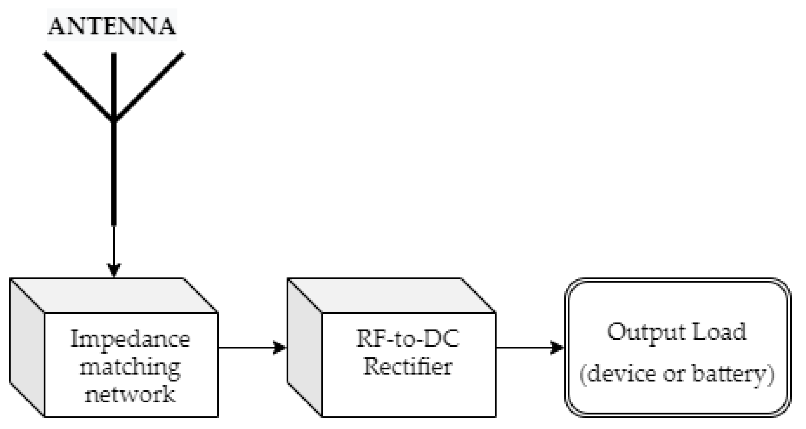
Figure 1. Basic block diagram of a rectenna system.
Telecom 02 00018 g001
Figure 2. The design process of the proposed Schottky diode-based rectifier.
Telecom 02 00018 g002
Figure 3. The generalized approach of a multiband rectenna system block diagram.
Telecom 02 00018 g003
Figure 4. The Greinacher voltage-doubler configuration.
Telecom 02 00018 g004
Figure 5. Proposed impedance-matching circuits of the dual- and triple-band rectifying circuits at: (a) 869 MHz and 940 MHz (dual-band); (b) 866 MHz, 948 MHz, and 2.423 GHz (triple-band).
Telecom 02 00018 g005
Figure 6. Basic topologies of two shunt combinations: (a) open-open; (b) open-shorted; (c) shorted-shorted.
Telecom 02 00018 g006
Figure 7. Flowchart for a typical genetic algorithm optimization.
Telecom 02 00018 g007
Figure 8. Obtained S11 parameter (reflection coefficient) of the proposed Schottky diode-based dual- and triple-band rectifier for R L = 13 kOhm (blue solid line: dual-band S11 parameter, green solid line: triple-band S11 parameter, red dash line: −10 dB limit).
Telecom 02 00018 g008
Figure 9. RF-to-DC efficiency vs. R L output load of the demonstrated (a) dual-band (for a two-tone signal: 869 MHz and 940 MHz) and (b) triple-band (for a three-tone signal: 866 MHz, 948 MHz, and 2.423 GHz) rectifying circuit for various RF input power values ( P i n ).
Telecom 02 00018 g009
Figure 10. (a) RF-to-DC efficiency vs. input power P i n ; (b) DC output voltage vs. the input power of the dual-band (two-tone signal: 869 MHz and 940 MHz) and the proposed triple-band (three-tone signal: 866 MHz, 948 MHz, and 2.423 GHz) rectifier for R L = 13 kOhm (blue solid line: dual-band, green solid line: triple-band).
Telecom 02 00018 g010
Figure 11. RF-to-DC efficiency versus frequency for various input power levels ( P i n ).
Telecom 02 00018 g011
Table 1. Physical dimensions of the microstrip lines for the impedance-matching network of Figure 5a: dual-band circuit (width/length values are expressed in mm).
ParameterWidth/LengthParameterWidth/Length
TL13/35TL63/35
TL23/4TL73/6
TL33/29TL83/17
TL41/3TL91/13
TL548/21TL1039/24
Table 2. Physical dimensions of the microstrip lines for the impedance-matching network of Figure 5b: triple-band circuit (width/length values are expressed in mm).
ParameterWidth/Length
TL113/39
TL123/24.3
TL133/25
TL141/7.5
TL1548/18.3
Table 3. Input impedance values of the dual- and triple-band rectifier, with and without the impedance-matching network.
Rectifier’s Input Impedance (Ohm)Frequency
(MHz)
% Deviation
from 50 Ohm
Real PartImaginary Part
without impedance matching
11.42−66.3686677.16
27.1−65.493745.8
with impedance matching
dual-band
(gradient optimizer)
44.36.186611.4
558.593710
triple-band
(genetic optimizer)
53.480.448666.96
48.819.669482.38
48.19−1.624233.62
Table 4. Comparative results of the proposed dual-band rectifier against related work.
Ref.Impedance
Matching
Schottky
Diode
Efficiency
@ Frequency
Input
Power
(dBm)
Load
(kOhm)
[8] *multistubHSMS285C24% @ 2.1 GHz
18% @ 2.45 GHz
10.01.60
[9] *cross- and
T-shaped
stubs
HSMS285057.60% @ 2.45 GHz
33.62% @ 5.8 GHz
30% @ 2.45 GHz
28% @ 5.8 GHz
0.0

10.0
2.00
[10] broadband
matching
network
HSMS285X∼68% @ 975 MHz
∼55% @ 1.9 GHz
−10.015.00
[11] open and
shorted
stubs
HSMS285063% @ 1.95 GHz
69% @ 2.5 GHz
7.0
3.5
1.00
[12] * λ /4 T-junction
and shorted
stubs
HSMS2822,
HSMS2852
66% @ 915 MHz
58% @ 2.45 GHz
∼30.0
∼31.0
0.62
4.70
[13] microstrip
line-based
HSMS2852,
HSMS285C
56.11% @ 2.67 GHz
57.95% @ 3.591 GHz
6.02.00
this work shunted
stubs
HSMS285C48% @ 866 MHz
65% @ 940 MHz
2.013.00
† simulated results, * measured results.
Table 5. Comparative results of the proposed triple-band rectifier against related work.
Ref.Sub.Impedance
Matching
Efficiency
@ Frequency
Input
Power
(dBm)
Load
(kOhm)
[15] FR-4microstrip
lines
42% @ 3-tone
signal 1.95 GHz
10.03.00
[16] *Duroid
5880
triple-stub,
tuning and
inductor
∼41% @ 925 MHz
∼32% @ 1.82 GHz
∼26% @ 2.17 GHz
−10.05.00
[17] FR-4meander line,
open and
radial stubs
68% @ 3-tone signal
2.0 GHz
2.47 GHz
3.6 GHz
−7.01.10
[18] Duroid
5880
open and
shorted stubs
61.9% @ 0.85 GHz
71.5% @ 1.77 GHz
60.5% @ 2.07 GHz
0.02.20
[19] *FR-4radial and
shorted stubs
54% @ 0.9 GHz
51% @ 1.8 GHz
48% @ 2.45 GHz
4.03.80
[20] *Duroid
5880
open and
shorted stubs
∼42% @ 1.85 GHz
∼45% @ 2.15 GHz
∼38% @ 2.48 GHz
∼48% @ 3-tone signal
−10.05.00
this work FR-4shunted stubs58% @ 866 MHz
68% @ 948 MHz
47% @ 2.423 GHz
81% @ 3-tone signal
0.013.00
† simulated results, * measured results.
Publisher’s Note: MDPI stays neutral with regard to jurisdictional claims in published maps and institutional affiliations.