Article

Reliability of Fine-Pitch Cu-Microbumps for 3D Heterogeneous Integration: Effect of Solder, Pitch Scaling and Substrate Materials

1
School of Mechanical Engineering, Purdue University, West Lafayette, IN 47906, USA
2
School of Material Science Engineering, Purdue University, West Lafayette, IN 47906, USA
*
Author to whom correspondence should be addressed.
Electron. Mater. 2025, 6(4), 18; https://doi.org/10.3390/electronicmat6040018
Submission received: 8 September 2025 / Revised: 19 October 2025 / Accepted: 23 October 2025 / Published: 3 November 2025

Abstract

A new and transformative era in semiconductor packaging is underway, wherein, there is a shift from transistor scaling to system scaling and integration through advanced packaging. For advanced packaging, interconnect scaling is a key driver, with interconnect density requirements for chip-to-substrate microbump pitch below 5 μm and half-line pitch below 1 μm for Cu redistribution layer (RDL). Here, we present a comprehensive theoretical comparison of thermal cycling behavior in accordance with JESD22-A104D standard, intermetallic thickness evolution, and steady-state thermal analysis of Cu-microbump assembly for different bonding materials and substrates. Bonding materials studied include solder caps such as SAC105 (Sn98.5Ag1.0Cu0.5), eutectic Sn-Pb (Sn63Pb37), eutectic Sn-Bi (Sn42Bi58), Pb95Sn5, Indium, and Cu-Cu TCB structure. Effect of substrates including Si, glass and FR-4 is evaluated for various microbump structures with varying pitches (85 µm, 40 µm, 10 µm, and 5 µm) on their fatigue life. Results indicate that for Cu-microbump assemblies at an 85 µm pitch. The Pb95Sn5 exhibits the longest predicted fatigue life (3267 cycles by Engelmaier and 452 cycles by Darveaux), while SAC105 shows the shortest (320 and 103 cycles). Additionally, the Cu-Cu TCB structure achieves an estimated lifetime of approximately 7800 cycles, which is significantly higher than all solder-based Cu-microbump assemblies. The findings contribute to advanced packaging applications by providing valuable theoretical references for optimizing solder materials and structural configurations.

1. Introduction

Since the inception of Moore’s Law in 1965, semiconductor integrated circuits (ICs) have consistently advanced in alignment with this principle for over half a century [1,2,3]. In 2022, both Samsung and TSMC announced the mass production of 3 nm process technology, marking a significant milestone as semiconductor fabrication nodes approach atomic-scale dimensions [4]. While transistor miniaturization has remained an effective strategy for enhancing chip integration and performance, it has also led to exponentially increasing costs and escalating technical challenges [5]. As Moore’s Law approaches its physical limitations, the demand for higher performance, lower power consumption, and more compact packaging has become increasingly pressing.
Advanced packaging technologies, particularly Chip-to-Substrate (C2S) interconnects, are emerging as critical enablers for the continued evolution of semiconductor technology in the post-Moore era. The interconnect pitch has shrunk from over 200 μm to below 10 μm, driving innovation and expanding applications in the semiconductor industry [6]. In the early stages of IC development, low integration density, limited input/output (I/O) pads, and large interconnect pitches positioned wire bonding and tape automated bonding as the predominant C2S interconnect technologies [7]. Technologies such as flip-chip and ball grid array (BGA) enabled the reduction of interconnect pitch to below 100 μm, significantly enhancing signal transmission speed and system performance [8]. From the 2000s to the 2010s, copper pillar bump (CPB) and microbump technologies gained traction, further advancing C2S interconnect technology [9]. Intel pioneered CPB technology for the 65 nm process of Yonah chips in 2006, reducing the interconnect pitch to 50 μm, markedly improving data transmission efficiency and heat dissipation performance [10]. TSMC has further demonstrated 20–40 μm Cu-microbump pitch and enhanced high-performance computing efficiency in its 20 nm and 16 nm processor chips [11]. Current technological trends emphasize thermocompression bonding (TCB) and hybrid bonding for advanced 3D IC stacking, with continued shrinking of interconnect pitch for C2S bonding [12]. Sony pioneered the application of these technologies in commercial production of stacked CMOS image sensors [13], integrating CPB and microbump technologies to achieve sub-10 μm pitch, with recent research demonstrating interconnect pitches as small as 0.5 μm [14,15]. Meanwhile, 3D ICs achieve ultra-high-density integration by stacking multiple chips and leveraging vertical interconnect technologies such as through-silicon vias (TSV), resulting in superior performance and reduced resistance-capacitance (RC) delay. NVIDIA has adopted 3D IC technology in its latest graphics processing units (GPUs), significantly enhancing processing capabilities and energy efficiency [16]. Although Cu-Cu hybrid bonding is well-suited for die-to-die, die-to-wafer, and wafer-to-wafer bonding, Cu-microbumps with solder TCB interconnect technology remain crucial for achieving high-density chip-to-substrate integration.
In advanced packaging systems, microbumps play a critical role as both electrical interconnects and mechanical support. However, reliability concerns can arise under thermal cycling conditions due to stress concentrations caused by mismatched coefficients of thermal expansion (CTE) among materials, leading to failures such as cracking, interfacial fracture, or solder cap fracture, compromising the device reliability [17]. Huang et al. systematically studied SAC305 (Sn96.5Ag3.0Cu0.5) microbump assemblies with four capping materials: Ni/Au, Sn, Sn-2.5Ag, and organic solderability preservative (OSP) [18]. Results showed that Cu-microbump structures treated with OSP capping exhibited superior structural integrity during thermal cycling, with no signs of cracking or void formation. Liu et al. investigated strain evolution and fatigue life in indium solder joints using finite element analyses (FEA) at various length scales, highlighting the impact of pitch scaling [19]. Similarly, Chen et al. demonstrated that increasing the height of high-lead solder joints improves reliability, though the effect is not strictly proportional [20]. Depiver et al. compared the creep fatigue behavior of lead-free SAC solders (SAC305, SAC387, SAC396, and SAC405) and lead-based eutectic solder based on various fatigue life prediction models [21].
The mechanical properties of microbumps are closely linked to intermetallic compound (IMC) characteristics, as IMCs serve as initiation sites for microcracks. The growth of IMCs degrades the mechanical integrity of interconnects, significantly reducing the fatigue life and solder joint strength, ultimately compromising reliability [22,23,24]. Chen et al. examined the relationship between IMC evolution and shear strength in Sn-Ag solder Cu-microbumps, showing that increasing IMC thickness weakens microbump strength [25]. Bertheau et al. further demonstrated that, beyond thickness, IMC composition and morphology also critically impact interconnect reliability [22]. Additionally, researchers have highlighted that IMC proportion has already become a key factor in solder joint failure, particularly in fine-pitch solder arrays [26,27,28]. When the IMC thickness is relatively thin (<1 μm), cracks typically initiate at the solder/IMC interface due to localized stress concentration. As thickness increases, residual stress from phase transformation further amplifies stress concentration, driving crack propagation into the solder and forming dimple fractures, which eventually evolve into cleavage fractures. Once the IMC exceeds 10 μm, the interface roughens significantly, leading to cleavage fractures [25,29]. Therefore, with the continued miniaturization and fine-pitch trends in bump technology, quantitatively determining IMC types and thicknesses is crucial for assessing reliability and lifetime prediction of microbump assemblies.
In this work, the structural reliability and failure mechanisms of Cu-microbump assemblies at varying interconnect pitches are analyzed using four solder types: lead-free solders (SAC105 and Sn42Bi58), lead-based eutectic solder (Sn63Pb37), high-lead solders (Pb95Sn5), and Indium. The Cu-Cu TCB structure is also examined in comparison with solder-based interconnections for die-to-substrate bonding. To ensure the accuracy of the predictions and to authentically reflect the mechanical behavior of microbump assemblies under thermal variations, IMC thickness is estimated using a diffusion-based kinetic model for the selected solder compositions. Additionally, considering the impact of CTE mismatch between the die and substrate on thermal fatigue life, substrate effects are incorporated to enhance the understanding of microbump reliability.

2. Finite Element Modeling and Scheme Design

2.1. Constitutive Equations

Solder joints in Cu-microbump assemblies experience combined elastic (reversible) and inelastic (irreversible) deformation during thermal cycling. The predominant inelastic deformation comprises both time-independent plasticity and time-dependent creep. From a continuum-mechanics perspective, both deformations originate from dislocation motion. To accurately capture the thermo-mechanical behavior of solder, the unified viscoplastic and constitutive model is employed [30], characterized by the following key features:
  • The model eliminates the need for explicit yield criteria and loading/unloading rules [31].
  • A single scalar internal variable represents the isotropic resistance to plastic flow, reflecting the material’s internal state [31].
And constitutive equation is formulated as follows [32]:
The deformation resistance is proportional to the equivalent stress:
σ   =   cs ,   c   <   1
where σ is the equivalent stress for steady plastic flow, c is the material parameter representing the strain rate function, and s is the deformation resistance with stress dimension. Under constant strain rate conditions, c can be expressed as:
c =   1 ξ sin h 1 ε ˙ p A exp Q RT m
where ξ is the stress factor, ε ˙ p is the effective inelastic strain rate, A is the pre-exponential factor, Q is the activation energy, R is the gas constant, T is the absolute temperature, and m is the strain rate sensitivity exponent.
Combining Equations (1) and (2), the flow equation of the Anand constitutive model adopts a hyperbolic sine law:
ε ˙ p   =   A exp Q RT sin h ξ σ s 1 / m
Additionally, the rate-dependent evolution of the internal variables is assumed to follow:
s ˙   =   h σ ,   s ,   T ε ˙ p
where the hardening function h   ( σ ,   s ,   T ) is related to the dynamic strain hardening and recovery process of the material, with its specific form as:
h =   h 0 1 s s * a   si nh 1 s s * ,   a     1
where h and a represent material strain hardening parameters, and s* is the saturation value of s.
By combining Equations (4) and (5), the specific form of the evolution equation for s can be obtained as:
s ˙   =   h 0 1     s s * a   si nh 1     s s *     ε ˙ p ,   a     1
s   ˙ = s ^ ε ˙ p A exp Q RT n
where s   ˙ describes the saturation value of s associated with a set of given temperature and strain rate, h0 is the hardening/softening constant, a is the strain rate sensitivity of hardening/softening, s ^ is a coefficient, and n is the strain rate sensitivity exponent of the saturation value of deformation resistance.
Based on Equations (2), (3), and (7), and σ* = cs*, the following equation can be derived:
σ *   =   c s *   =   s ^ ξ ε ˙ p A exp Q RT n sin h 1 ε ˙ p A exp Q RT m
This equation is related to the saturation stress, temperature, and strain rate. Under isothermal conditions where s* > s, by combining Equations (4) and (8), the following equation can be obtained:
d σ d ε p   =   c h 0 1     σ σ * a   si nh 1     σ σ * ,   a     1
Further integrating Equation (9), the general form of the Anand viscoelastic constitutive model, which integrates the preceding flow and hardening relations, can be expressed as:
σ   =   σ *     σ *     c s 0 1 a   +   a 1 c h 0 σ * a ε ˙ p 1 / 1 a ,   a     1
where σ0 = cs0, and s0 represents the initial deformation resistance.
The viscoplastic and constitutive model thus includes nine parameters: s0, Q, A, ξ, m, h0, s ^ , n, and a, which are defined in the material property module for implementation. The specific values for the solder used in this study are provided in Table S1 [19,33,34,35,36].

2.2. Finite Element Analysis

The FEA models for the Cu-microbump assembly and Cu-Cu TCB structure were developed using the SpaceClaim module within ANSYS Workbench 2023. The global model consists of 256 microbumps arranged in a 14 × 14 matrix with an 85 μm interconnect pitch, with detailed geometric parameters summarized in Table 1. To optimize computational efficiency while maintaining accuracy, a local model was strategically extracted from the global configuration by leveraging the inherent symmetry of the microbump array. The geometric structures of both the global and local models are depicted in detail in Figure 1. The Cu-microbump assembly features a nine-layer architecture comprising the die, Cu-trace, Cu-pillar, diffusion barrier, upper IMC layer, solder, lower IMC layer, Cu-pad, and substrate. Each pair of pillars is connected by a trace, forming groups that are further linked via Cu-metal lines embedded in the substrate, completing the daisy-chain interconnection. The Cu-Cu TCB structure consists of an upper Cu-layer, a lower Cu-layer, and a Cu-pad, forming a direct metallic bond without an intermediate solder layer. To accurately capture stress distribution and failure mechanisms, appropriate material properties were assigned. Most materials were treated as isotropic, linear elastic, with properties shown in Table 1. For the copper material, a bilinear isotropic plasticity model is employed, with a yield strength and tangent modulus of 172.3 MPa and 517 MPa [37]. In addition to the material parameters presented in this section, a comprehensive summary of representative solder alloys is provided in Table S2 of the Supplementary Information (SI), which compiles their composition, melting point, typical application, and key findings from the previous literature to provide a clear reference for the subsequent reliability comparison and discussion.
Meshing was performed using Hypermesh, and the generated mesh was imported into ANSYS Workbench as an .inp file for finite element analysis. The model employs Solid186 20-node hexahedral elements with an average size of 2.03 μm, with the local model consisting of 2,397,229 nodes and 1,915,618 elements for thermo-mechanical analysis. A mesh independence study, shown in Figure S1, confirmed sufficient convergence at this resolution, which was adopted for all subsequent analyses.
In this study, temperature cycling was applied as the loading condition following the JEDEC JESD22-A104D standard [51]. The temperature range spanned −55 °C to +125 °C, with a cycle duration of 34 min, a temperature change rate of 15 °C/min, and dwell times of 5 min at both extremes. The initial reference temperature for the zero-stress state was set at 25 °C (room temperature). Since thermal fatigue life prediction for solder joints typically relies on the range of equivalent plastic strain and plastic strain energy density observed during the initial thermal cycles. These ranges tend to stabilize after the 4th or 5th cycle for most solder materials, enabling reliable life estimation based on their stabilized values, so the simulation was conducted over six cycles. The specific temperature profile is illustrated in Figure S2a. To accurately represent the characteristics of the thermal load, 35 load steps were employed in this simulation. The number of sub-steps within each load step is determined through step-size sensitivity analysis, ensuring convergence and reliable results.
FEA was performed using the local model, with symmetric boundary conditions applied at the cut boundaries to accurately capture the mechanical response of the global model. To account for potential substrate warpage, fixed constraints were imposed in the x, y, and z directions at the center of the model’s bottom surface to prevent rigid body motion, specifically at the corner of the local model. The boundary and loading conditions are shown in detail in Figure S2b.

2.3. Lifetime Prediction Models

During thermal cycling, solder layers in microbump structures experience repetitive deformation due to thermal stress, leading to the progressive accumulation of internal damage that results in crack initiation and propagation. This study employs two life prediction models, the Engelmaier-modified Coffin–Manson model [52,53] and the Darveaux model [54], to evaluate the fatigue life of various solder materials under thermal cycling. The Engelmaier model is based on fracture toughness criteria, primarily predicting fatigue life based on plastic strain while accounting for temperature and thermal effects, as expressed by the following equation:
N f   =   1 2 Δ γ 2 ε f 1 / c
where Nf represents the fatigue life of the solder joint, Δγ denotes the range of shear plastic strain, given by Δ γ   =   3 Δ ε and Δ ε   signifies the range of equivalent plastic strain. εf is the fatigue ductility coefficient, while c is the fatigue ductility exponent, which depends on temperature and frequency.
In comparison, the Darveaux model incorporates both creep and fatigue interactions, predicting fatigue life based on energy density. This model integrates both crack initiation and propagation, addressing the limitations of earlier energy-based fatigue models that focus solely on crack initiation. The failure cycle life in the Darveaux model is the sum of the cycles required for crack initiation and those needed for complete crack propagation to failure [55]. The specific formulas are as follows:
N 0   =   k 1 Δ W ave k 2
da dN = k 3 Δ W ave k 4
N a   = a da / dN
N f   = N 0   + N a
where Nf denotes the characteristic fatigue life of the solder joint, N0 represents the number of cycles to crack initiation, and Na is the number of cycles for complete crack propagation. The parameters K1, K2, K3, and K4 are experimentally determined constants, and ΔWave is the average inelastic strain energy density increment, expressed as:
Δ W ave = i = 1 n v i Δ W i i = 1 n v i
where vi is the volume of the ith element, and ΔWi is its corresponding inelastic strain energy density. The FEA implementation for predicting the fatigue life of Cu-microbump assemblies is shown in Figure S3.
This study investigates the reliability of microbump interconnect structures with an 85 μm pitch, focusing on four solder types: lead-free solders (SAC105 and Sn42Bi58), lead-based eutectic solder (Sn63Pb37), high-lead solder (Pb95Sn5), and Indium solder. Key mechanical parameters, including maximum equivalent stress, equivalent plastic strain, and strain energy density, were extracted from the corresponding FEA models to systematically evaluate thermo-mechanical behaviors and failure modes under thermal cycling, as shown in detail in Table S3. To investigate scaling effects in fine-pitch models, global-local simulations were conducted for SAC105, Indium, Sn63Pb37, Pb95Sn5, Sn42Bi58 solders, and Cu-Cu TCB at pitches of 85 μm, 40 μm, 10 μm, and 5 μm, following Saint–Venant’s principle (Figure 1c) [56,57]. To ensure consistency in variables, all models maintained a constant total interconnect area and aspect ratio under identical loading and boundary conditions, resulting in an increase in the number of microbumps as the pitch decreased. To examine substrate effects, FEA models were developed for the same pitch sizes across Si, glass, and organic substrates to assess the impact of CTE mismatch on interconnect lifetime and substrate warpage. Steady-state thermal analysis further examined temperature gradient and heat flux distribution across different substrates and solders, providing a foundation for experimental validation and optimization.

2.4. IMC Growth Kinetics

As electronic devices continue to miniaturize, IMCs play an increasingly critical role in interconnect reliability [58]. Accurate estimation of IMC thickness is therefore essential for evaluating the service life and reliability of interconnect structures. The growth kinetics of interface IMCs typically adhere to either linear or parabolic diffusion laws. A linear relationship between IMC growth and reaction time indicates an interface–controlled process, whereas a parabolic relationship suggests diffusion–controlled growth [59]. In the Cu-Sn system, where the aging temperature is lower than the melting point of the reacting components, IMC formation predominantly occurs through solid-state diffusion. In this study, with thermal stress as the sole external load, atomic diffusion and IMC growth are primarily driven by thermally induced diffusion resulting from the temperature gradient. Therefore, the IMC growth parameters for the studied solders are determined using the empirical power-law equation and the Arrhenius equation, expressed as [60,61]:
d   =   d 0   +   Dt
D = D 0 exp ( Q RT )
The thickness of the IMC layer is proportional to the square root of the thermal aging time. In the above equations, d represents the IMC thickness at time t during thermal aging, d0 is the initial IMC thickness, D is the thermal diffusion coefficient, t is the duration of thermal aging, D0 denotes the diffusion constant, Q is the activation energy for IMC growth, R is the gas constant (8.314 J·mol−1·K−1), and T is the absolute temperature.
Lead-free solders (SAC105 and Sn42Bi58) and lead-based eutectic solder (Sn63Pb37) primarily form Cu6Sn5 IMCs, while high-lead solder (Pb95Sn5) predominantly forms Cu3Sn. Under identical conditions, Indium solder generates Cu11In9 IMCs. Since SAC, tin-bismuth, and eutectic tin-lead solders may simultaneously form both Cu6Sn5 and Cu3Sn during thermal aging [62,63,64,65,66], a combined IMC thickness is incorporated into the FEA model.
Following the identification of IMC types, the IMC thickness for each solder is calculated using Equations (17) and (18). To minimize the influence of reflow processes, surface treatments, and interface cleanliness on IMC formation and growth, while ensuring consistency in kinetic parameters, the initial IMC thickness (d0) is set to 0, the thermal aging duration (t) is set to 1389 h, and the absolute temperature (T) is set to 373 K. Due to limited studies on IMC formation in high-lead solders at 100 °C, the IMC thickness for Pb95Sn5 is estimated based on existing data at 150 °C (Figure S4), and the primary calculation steps are detailed in the SI [62,67,68].
Based on the reported values of D100 °C and Q100 °C [67,68], the IMC thickness evolution with thermal aging time was plotted for five solder types (Figure S4d). The results show an initial rapid increase in IMC thickness, followed by a gradual deceleration as the growth stabilizes. Among the solders, Indium exhibits the most significant IMC thickening, likely due to its high reactivity with Cu and low melting point, allowing more time for Cu11In9 phase formation, which promotes the formation of a thicker IMC layer. Rodrigues et al. observed that Indium additions to SAC solder enhance fracture toughness and shear strength while increasing IMC thickness [69]. In terms of lead-free solders, a higher Sn content leads to more substantial IMC growth during thermal aging compared to high-lead solders. Due to the limited availability of IMC kinetic parameters for Sn42Bi58 in existing research, an IMC thickness of 1 μm is used, estimated based on a diffusion coefficient of 1.84 × 10⁻¹⁹ m2/s. The specific IMC thickness values are summarized in Table 2.
Upon completing the IMC thickness calculations, the data were integrated into the corresponding solder microbumps to finalize the FEA model.

3. Effect of Cu-Microbump Pitch on Thermal Cycling Behavior

3.1. Failure Mode Analysis

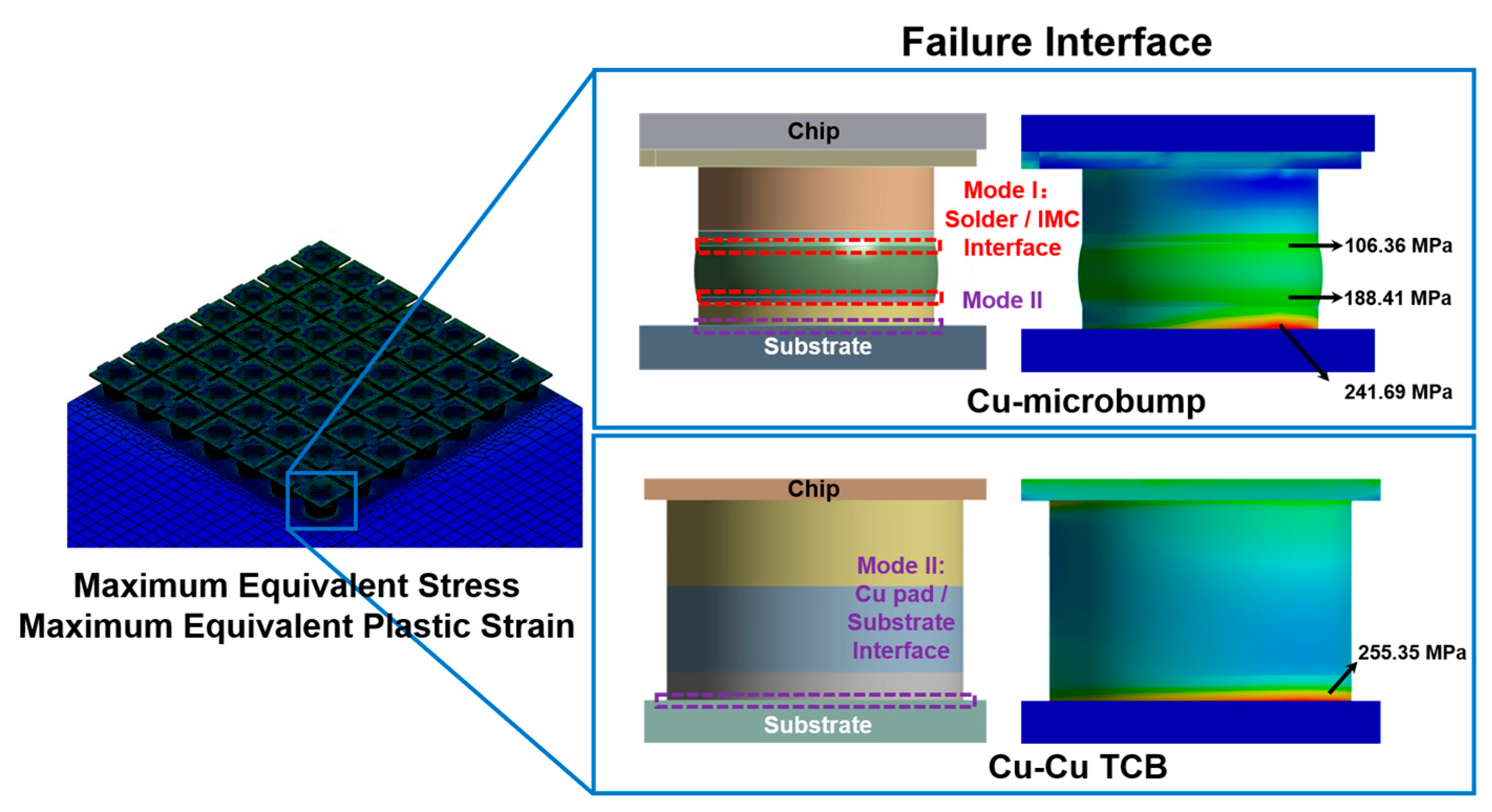
During thermal cycling in microbump assemblies, maximum damage localizes at corner solder bumps due to synergistic effects of stress concentration, CTE mismatch, and thermal gradients. Geometric discontinuities at corners amplify localized stress concentration, while CTE mismatch between materials drives plastic deformation. Enhanced thermal gradients at corners further exacerbate differential expansion/contraction, compounded by inherent weaknesses at the bump–substrate interface. These factors collectively render corner bumps more susceptible to fatigue failure, thereby establishing them as critical sites for fatigue life evaluation [71]. FEA reveals two dominant failure modes in Cu-microbump systems: (1) Mode I: Solder-IMC interfacial failure. IMC exhibits a higher Young’s modulus (Table 1) and a lower strain to failure compared to ductile solder alloys, promoting brittle fracture at interfaces. CTE mismatch-induced thermal stress concentration is primarily observed at the solder/lower IMC interface, which promotes crack nucleation and interfacial delamination (Figure 2). (2) Mode II: Cu-pad/substrate interfacial failure due to the CTE mismatch between Cu and substrate. Geometric discontinuities at the Cu-pad edge intensify stress concentrations, yielding a maximum equivalent stress of 241.69 MPa (Cu-pad/substrate) under thermal extremes. For the Cu-Cu TCB structure, thermal loading induces a stress concentration of 255.35 MPa at the Cu-microbump/substrate interface (Figure 2) due to the difference in thickness and planar dimensions of the die and substrate. This localized stress concentration can result in interface cracking at the microbump-under-bump metallurgy (UBM) interface.

3.2. Multiphysics Field Distributions in Critical Microbump

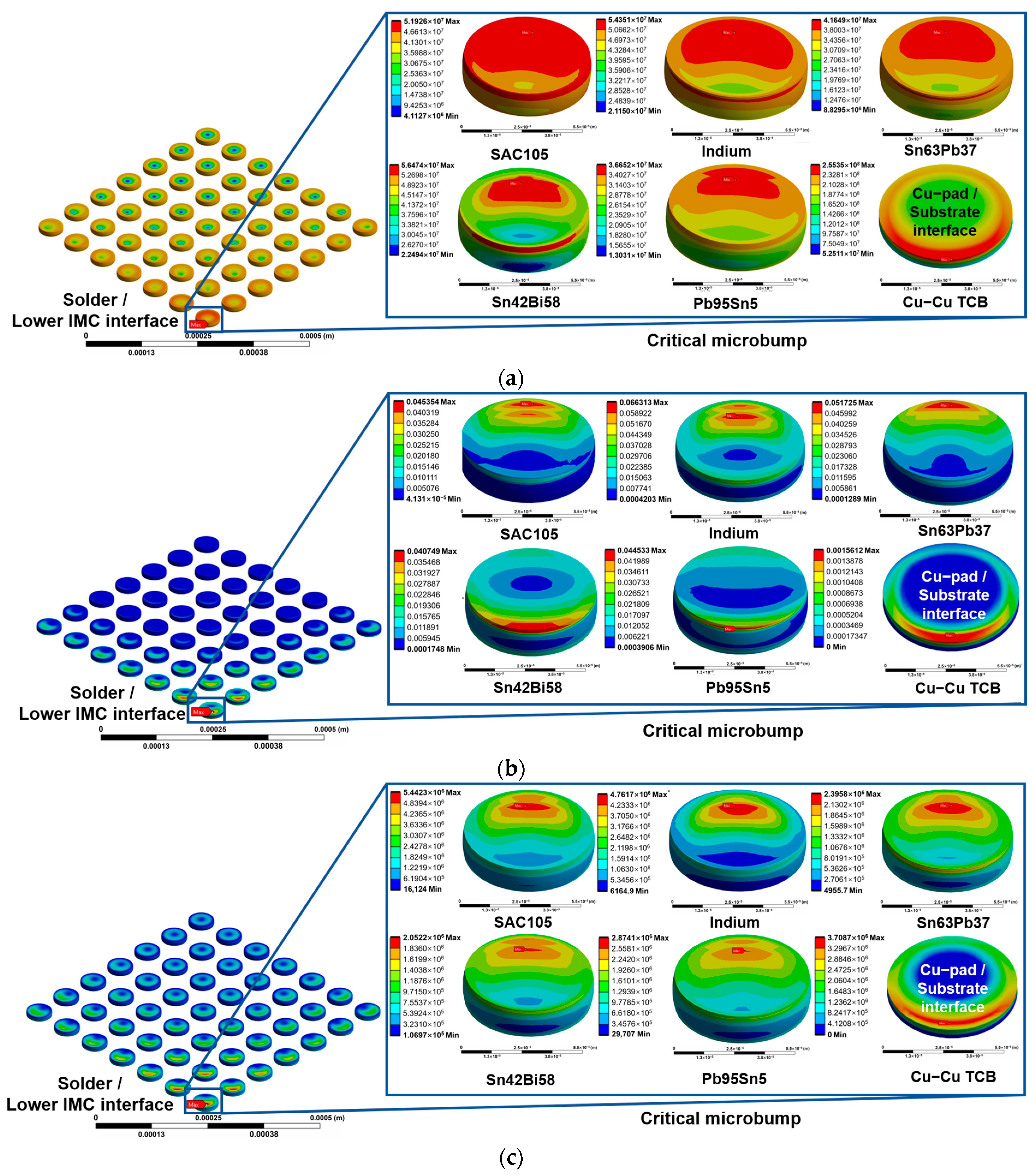
Figure 3a illustrates the maximum von Mises stress distribution in the critical microbump across five Cu-microbump assemblies and Cu-Cu TCB structure during the sixth thermal cycle. The maximum stress is localized at the outermost Cu-microbump in all scenarios, aligning with previous research findings on solder joints [71]. Among the evaluated solder alloys, Sn42Bi58 exhibited the highest stress concentration of 56.47 MPa, while Pb95Sn5 demonstrated the lowest value at 36.65 MPa. Stress analysis of the critical microbump reveals stress concentration along the outer edge of the solder/IMC interface. Thermal cycling induces progressive stress redistribution toward the central region, intensifying interfacial stress gradients, promoting crack nucleation at the interface periphery, followed by inward propagation under cyclic loading. In the case of Cu-Cu TCB structure, peak stress concentration of 255.35 MPa is observed at the outer-ring region of the Cu-pad/substrate interface, significantly larger than the solder-based structure (Figure S5a).
Figure S6a illustrates the temporal evolution of von Mises stress at the critical microbump, showing progressive accumulation with each thermal cycle, exhibiting a diminishing rate of increase that asymptotically approaches convergence. During cooling phases, an increase in contact stiffness and elastic modulus drives stress concentration, with SAC105 exhibiting a peak stress of 51.92 MPa. Conversely, heating phases induce stress relaxation due to reduced elastic modulus, lowering stress in SAC105 to 2.87 MPa. This cyclic asymmetry underscores the temperature-dependent stress behavior, where lower temperatures exacerbate crack initiation risks through intensified stress accumulation. Notably, Sn42Bi58 and Indium exhibit distinctly different stress evolution behaviors during thermal cycling. Indium, characterized by the highest CTE of 32 ppm/°C among all solders, generates substantial initial thermal stresses during cooling. However, its superior ductility enables stress dissipation through relaxation at elevated temperatures and plastic deformation at low temperatures, ultimately maintaining residual stresses below 20 MPa after the second thermal cycle, as shown in Figure S6b. In contrast, Sn42Bi58 demonstrates limited plasticity, leading to pronounced early-cycle stress accumulation of 56.42 MPa. Progressive plastic deformation in subsequent cycles partially relieves stress, yet constrained relaxation effects gradually diminish the effectiveness of stress relaxation.
Figure 3b shows the maximum equivalent plastic strain distribution in the critical microbump across five Cu-microbump assemblies and Cu-Cu TCB structure during the sixth thermal cycle. Maximum plastic strain localizes at the solder/IMC interface in the critical microbump, spreading progressively from the periphery to the central region, consistent with the stress distribution patterns. Among the solder alloys, indium demonstrates the highest strain value of 0.066131, while Sn42Bi58 shows the lowest strain value of 0.040739. Figure S7a illustrates the temporal evolution of plastic strain at the maximum strain location, revealing cyclic fluctuations synchronized with stress variations. This cyclic stress-strain coupling induces progressive fatigue damage, ultimately leading to microbump failure. Notably, the equivalent plastic strain range stabilizes after the fourth or fifth thermal cycle, allowing fatigue life prediction based on the stabilized strain range extracted from the sixth cycle. In contrast, Cu-Cu TCB structure exhibits its maximum equivalent plastic strain during the first thermal cycle, with a peak value of 0.00156 (Figure S7b), which is approximately one order of magnitude lower than that of solder-based microbumps. Copper experiences relatively pronounced plastic deformation during the initial thermal cycles. However, plastic strain stabilizes in subsequent cycles due to strain hardening.
Figure 3c shows the maximum strain energy density distribution in the critical microbump across five Cu-microbump assemblies during the sixth thermal cycle. The critical microbump exhibits maximum strain energy density localization at the solder/IMC interface, with strain energy spreading from the outer edge toward the central region, consistent with the spatial patterns of stress and strain distributions. Among the solder alloys, SAC105 demonstrates the highest strain energy density of 5.44 × 10⁶ J/m3, while Sn42Bi58 shows the lowest value of 2.05 × 10⁶ J/m3. Figure S8a depicts the temporal evolution of strain energy density at the maximum energy location, which increases linearly with the number of thermal cycles, with SAC105 showing the highest increase. Notably, the strain energy range stabilizes between the second and third thermal cycles. Based on this stabilization behavior, the fatigue life of the microbump is estimated to use the inelastic strain energy density range in the sixth cycle. For the Cu-Cu TCB structure, the strain energy density exhibits an overall parabolic trend, progressively approaching a stable plateau with increasing thermal cycles (Figure S8b). Further details on the equivalent stress, equivalent plastic strain, and strain energy density across different interconnect pitches are provided in Table S3.

3.3. Thermal Fatigue Life Prediction

The fatigue life of five solder alloys was predicted in this study through comparative application of the Engelmaier model (Equation (11)) and the Darveaux model (Equations (12)–(16)). In the Engelmaier framework, the fatigue ductility coefficient (εf) and exponent (c) were assigned values of 0.325 and −0.442 for lead-based alloys, and 0.325 and −0.4213 for Indium [34,72,73]. Lead-free solders utilized modified parameters (εf = 0.24, and c = −0.5708) to account for their unique fatigue response [74]. In the Darveaux model, the constants K1, K2, K3, and K4, derived from experimental fitting, are listed in Table 3 [75,76,77,78]. Given that the current research into constitutive relationships on tin-bismuth solder is limited, further studies are necessary to accurately determine the constants required for its fatigue life prediction using the Darveaux model. Therefore, fatigue-life predictions for Sn42Bi58 were derived exclusively from plastic strain analysis.
The Engelmaier–modified Coffin–Manson and Darveaux fatigue life prediction models were applied to each solder material, as illustrated in Figure 4. The results indicate that SAC105 exhibits the shortest fatigue life, followed by Indium and Sn42Bi58. Lead-based solders demonstrate superior fatigue resistance: Sn63Pb37 outperforms the aforementioned alloys, while Pb95Sn5 achieves the longest fatigue life, with Engelmaier model predictions reaching 3267 cycles. SAC alloys exhibit significant plastic deformation under high stress-strain conditions, accelerating fatigue damage accumulation. In contrast, high-lead solders exhibit minimal stress concentration due to their high stiffness and creep resistance. Notably, predictions from the Engelmaier and Darveaux models diverge substantially, with fatigue life estimates differing by a factor of 3–7. The Engelmaier model, dependent on strain amplitude and ductility parameters, shows high sensitivity to inelastic shear strain variations, potentially overestimating life in cases with significant CTE-mismatch-induced shear deformation. Conversely, the Darveaux model, grounded in plastic work and energy distribution principles, provides more conservative predictions.
Coffin–Manson model [79,80] is used to predict the thermal fatigue life of Cu-Cu TCB structure, with primary focus on low-cycle fatigue (LCF) dominated by plastic strain, without explicitly accounting for creep–fatigue interactions. Given that the thermal cycling temperature profile in this study ranges from −55 °C to 125 °C, the creep effects in copper are relatively insignificant. Hence, fatigue life within this temperature range is predominantly governed by plastic deformation, making the Coffin–Manson model appropriate for fatigue life prediction.
N f = C Δ ε i m
The fatigue life (Nf) is calculated using the fatigue ductility coefficient (C) and the equivalent plastic strain range per cycle (Δεi), with m as the fatigue exponent. For Cu, C is set to 2.18 and m to −0.66 [81]. Since the equivalent plastic strain range stabilizes between the fourth and fifth cycles, a stabilized value of Δεi = 4.13 × 10⁻⁶ is extracted. Substituting all these values into Equation (19) yields a fatigue life of 7797 cycles for the Cu-Cu TCB structure. Compared to solder-based microbump assemblies, the Cu-Cu TCB structure demonstrates significantly enhanced fatigue resistance, primarily attributed to the superior mechanical properties of Cu [37].

3.4. Pitch Effect on Lifetime Prediction

The thermal fatigue life of Cu-microbump with five solders and Cu-Cu TCB structure at various interconnect pitches (85 μm, 40 μm, 10 μm, and 5 μm) is estimated and compared using the Engelmaier and Darveaux models, as shown in Table 4. A significant reduction in estimated fatigue life is observed with decreasing interconnect pitch. SAC105 exhibits the shortest lifetime across all pitches, with Engelmaier model predictions declining from 320 cycles at 85 μm to 29 cycles at 5 μm, and Darveaux model predictions dropping from 103 cycles to 1 cycle, due to limited plastic deformation. In contrast, Indium demonstrates enhanced stress redistribution capabilities at 40 μm pitch due to its high ductility (σvM = 64.32 MPa), resulting in extended service life. Sn42Bi58, Sn63Pb37, and Pb95Sn5 exhibit progressively improved fatigue resistance, with Pb95Sn5 achieving the longest lifetime among Cu-microbump assemblies, attributed to its exceptional toughness. Cu-Cu TCB structure outperforms all solder-based interconnects, demonstrating the highest fatigue life across all pitches, as evidenced by Coffin–Manson predictions declining from 7797 cycles at 85 μm to 2163 cycles at 5 μm pitch. Figure S9 shows the predicted decrease in solder fatigue life with decreasing interconnect pitch based on both fatigue models. The Engelmaier model, based on strain-controlled fatigue, is more sensitive to variations in strain amplitude, whereas the Darveaux model, which considers strain energy dissipation, provides more conservative lifetime predictions. Some studies suggest that the Engelmaier model yields more conservative lifetime estimates than the Darveaux model [82], whereas others report the opposite [83]. In this study, the Darveaux model predicts shorter fatigue lifetimes under fine-pitch and high-stress conditions. It should be noted that although a small pitch allows the applied load to be distributed among more microbumps on a global scale, the reduced bump size at fine pitches increases the local geometric constraint and intensifies stress and strain concentration at the critical bumps. During thermal cycling, the CTE mismatch among different materials induces substrate warpage, which amplifies the thermal stress and strain in the outermost and corner regions. In addition, the creep–fatigue interaction under cyclic thermal loading further accelerates the accumulation of inelastic strain and crack propagation, leading to a reduced fatigue lifetime for fine-pitch interconnects.
Among the three fatigue life prediction models employed in this study, the Darveaux model most accurately reflects the actual service behavior of microbump interconnects with solder assembly under thermal cycling. This model incorporates both plastic deformation and creep effects through the inelastic strain energy density, enabling a simultaneous description of the crack initiation and propagation mechanisms that dominate microbump failure. From a mechanistic standpoint, this energy-based framework provides a more realistic representation of the actual evolution of fatigue damage compared with the strain-based Engelmaier model, which is suitable for low-cycle fatigue analysis but tends to overestimate the lifetime when creep-fatigue interaction becomes significant. In contrast, for Cu-Cu TCB structures, where deformation is primarily governed by plastic fatigue and the effect of creeping is negligible, the Coffin–Manson model remains the most appropriate approach for fatigue life estimation.

3.5. Substrate Effect on Lifetime Prediction

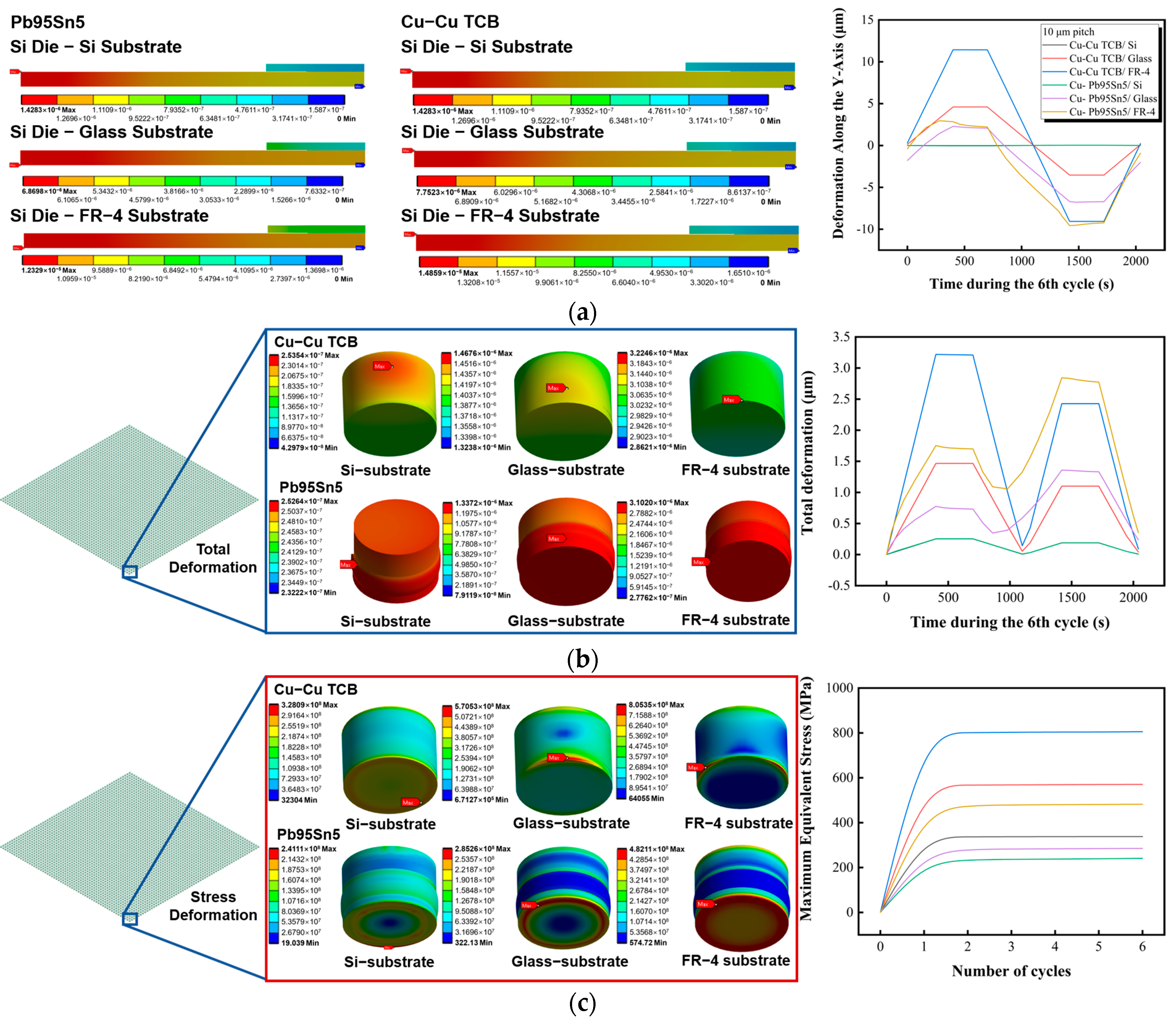
The differential thermal expansion in microbump assemblies caused by CTE mismatch among the die, microbump interconnects, and substrate induces structural warpage under cyclic thermal stress. Such warpage deformation may critically affect assembly reliability. This study systematically examines the thermo-mechanical response and fatigue lifetime of the microbump structure with three substrate materials (Si, glass, and organic) under a 10 μm pitch condition. The simulation uses Pb95Sn5 solder and a Cu-Cu TCB structure, maintaining component dimensions consistent with those in previous sections, while the substrate material properties are detailed in Table 2. Figure 5a illustrates the total deformation distribution in Pb95Sn5-based microbumps and Cu-Cu TCB with three distinct substrate materials. All configurations exhibit maximum deformation at substrate corner regions. In the Si-substrate assembly, material homogeneity between die and substrate eliminates most of the CTE mismatch, producing a uniform stress distribution and resulting in minimal deformation of 1.42 μm. Comparatively, glass and organic substrates exhibit amplified CTE values relative to Si, driving asymmetric thermal expansion gradients. This mismatch mechanism induces concentrated stress fields at substrate corners, with deformation magnitudes reaching 6.86 μm for glass and 12.32 μm for organic substrates. Relatively, the Cu-Cu TCB structure exhibits a comparable total deformation of 1.42 μm for the Si-substrate, but slightly increased deformation of 7.75 μm for the glass and 14.85 μm for the organic substrates.
The deformation characteristics of substrates critically influence the shape evolution of microbumps during thermal cycling. A quantitative analysis of total deformation distribution and maximum equivalent stress evolution was performed on the critical microbump using three substrate configurations, as detailed in Figure 5. In Pb95Sn5-based microbump assemblies with glass and organic substrates shown in Figure 5b, the total deformation during the cooling phase is greater than that during the heating phase, with the maximum values reaching 2.41 μm and 2.85 μm. This behavior originates from the significant CTE mismatch between the die, substrate, and interconnect bumps. The constrained horizontal expansion induces compressive stress at both the die and substrate interfaces, which are further amplified by the combined effects of the microbump interconnect geometry and mechanical constraints, ultimately leading to a convex-down curvature with central deflection surpassing edge regions for glass and organic substrates. Conversely, Si-substrate assemblies exhibit minimal deformation (maximum of 0.25 μm), producing a slightly concave-up curvature with peripheral deflection exceeding that of the central regions. However, for the Cu-Cu TCB structure, the deformation trend is reversed, with the total deformation during the cooling phase being lower than that during the heating phase. The maximum deformations observed for assemblies utilizing glass and organic substrates were 1.46 µm and 3.22 µm, both slightly exceeding the corresponding values observed in the Pb95Sn5-based microbump, with minimal deformation of 0.25 µm for the Si substrate, indicating negligible structural warpage during the thermal cycling.
The evolution of maximum equivalent stress in the critical microbump with the number of thermal cycles is shown in Figure 5c. The Si-substrate assembly exhibited the lowest stress level, with peak equivalent stresses of 241.11 MPa for the Pb95Sn5-based microbump assembly and 338.15 MPa for the Cu-Cu TCB structure. Comparatively, the glass and organic substrate assemblies exhibited substantially higher stress variations, with maximum equivalent stresses of 285.26 MPa and 482.11 MPa for Pb95Sn5-based microbump assemblies, and 570.53 MPa and 805.35 MPa for Cu-Cu TCB structure. The exceptionally high equivalent stress observed in the Cu-Cu TCB structure exceeds the typical ultimate tensile strength (UTS) of copper, primarily due to the absence of damage criteria in the current model. Although bilinear plasticity is applied, stress continues to accumulate at this potential damage site under thermal cycling without failure modeling.
Figure 6 shows a comparison of estimated fatigue life using Engelmaier, Darveaux, and Coffin Manson models, revealing substantial lifetime variations across substrate types. Substrates with higher CTE induce greater thermo-mechanical stresses and deformations in microbumps, directly accelerating failure mechanisms and reducing operational lifetime relative to Si-substrate assembly.

4. Thermal Performance Analysis

Electronic device thermal management predominantly relies on convective heat transfer rather than radiative mechanisms, as reflected in the substrate model, which exclusively considers convective exchange with ambient air. This paper adopts a simplified thermal framework by neglecting external perturbations and assuming the die as a constant-temperature heat source at 125 °C with stable thermal dissipation. Internal heat transfer follows Fourier’s conduction law across material interfaces, while external surfaces obey Newton’s cooling law with ambient temperature maintained at 25 °C. The convective heat transfer coefficient is specified as 10 W/m2·°C [45] with substrate bottom surfaces thermally anchored to ambient conditions. Component thermal conductivities for this steady-state model are summarized in Table 1, with detailed boundary conditions and thermal loading schematics presented in Figure S10.
Figure 7a–c comparatively illustrates the temperature distribution along the arc length of the Cu-microbump assembly during steady-state thermal conduction among various substrate materials and solder types. In Si-substrate assembly, the high thermal conductivity of Si enables efficient heat dissipation, allowing observable thermal gradients along microbump arc length with the choice of solder materials. Sn42Bi58 solder alloy, characterized by its relatively low thermal conductivity (17 W/m·°C), induces a substantial temperature gradient, whereas Cu-Cu TCB promotes a more gradual temperature transition. Conversely, assemblies employing glass and organic substrates are limited by thermal gradients in the substrate due to their inherently lower thermal conductivities.
Figure 7d–f illustrates the steady-state thermal characteristics of Cu-microbump across three substrate configurations through temperature, heat flux, and temperature gradient distributions. The temperature drop across the microbump arc length (TmaxTmin) is observed as 50.85 °C, 0.71 °C, and 0.22 °C for Si, glass, and organic substrates. Glass and organic substrates with lower thermal conductivity result in a higher operating temperature of the Cu-microbump assembly. Table S3 presents the impact of varying solder thermal conductivity on heat flux and temperature gradient distributions in Cu-microbump assembly. As the thermal conductivity of solders increases from 58 W/m·°C to 400 W/m·°C, the heat flux within the Si-substrate assembly exhibits a substantial increase from 4.25 × 10⁸ W/m2 to 5.70 × 10⁸ W/m2 before gradually stabilizing. This contrasts sharply with glass and organic-substrate assemblies, where flux densities remain relatively constant from 1.018 × 10⁷ W/m2 to 1.021 × 10⁷ W/m2 and 3.107 × 10⁶ W/m2 to 3.110 × 10⁶ W/m2 (Figure S11a). Both cases exhibit negligible sensitivity to solder conductivity variations. The Silicon, due to its intrinsic high thermal conductivity (147 W/m·°C), achieves optimal heat transfer efficiency when paired with high-conductivity solder, whereas glass and organic materials demonstrate limited responsiveness to solder conductivity changes, as also shown in Figure S11.

5. Conclusions

This study comprehensively investigates the thermo-mechanical reliability of Cu-solder and Cu-Cu TCB microbump interconnects under thermal cycling and steady-state thermal conditions with a focus on solder types, interconnect pitch, and substrate materials. IMC thickness growth is estimated based on power-law diffusion kinetics of Cu into the solders, which is incorporated into the calculation of microbump fatigue life. The results indicate that the highest stress concentration in Cu-microbump assembly primarily occurs at the solder/IMC interface, whereas for the Cu-Cu TCB structure, failure is more likely to initiate at the Cu-pad/substrate interface. Among the evaluated solder materials, SAC105 exhibited the shortest fatigue life, whereas Pb95Sn5 achieved the longest, with the Engelmaier model predicting a lifetime of 3267 cycles and the Darveaux model estimating 452 cycles. Compared to the strain-controlled Engelmaier model, which is more sensitive to strain amplitude variations, the Darveaux model based on strain energy dissipation provides a more conservative lifetime prediction accounting for creep-fatigue deformation. Additionally, the results showed a significant pitch effect on thermal cycling reliability, wherein reducing the pitch from 85 μm to 5 μm led to a more than 73.7% reduction in fatigue life across all solder materials. However, the Cu-Cu TCB structure consistently exhibited the highest thermal cycling reliability across all pitch sizes, demonstrating a significantly longer fatigue life based on the Coffin–Manson fatigue model. Furthermore, substrate materials were found to have a substantial impact on reliability. Due to its excellent CTE matching the die, the Si-substrate exhibited the longest fatigue life, corresponding to the lowest warpage, whereas glass and organic substrates, with higher CTE mismatches, introduced greater thermal stresses and higher failure risks. Steady-state thermal analysis further confirmed that the Si-substrate provided the best thermal management performance, effectively reducing temperature gradients and enabling more uniform heat dissipation across the package. These theoretical results provide a valuable reference for existing research and support the optimization of solder selection, structural design, and thermal management strategies in advanced packaging applications. Next steps include experimental validation of promising bonding methodologies for 3D heterogeneous integration for various substrate and die materials.

Supplementary Materials

The following supporting information can be downloaded at: https://www.mdpi.com/article/10.3390/electronicmat6040018/s1, Figure S1: The relationship between the number of elements and the maximum equivalent stress; Figure S2: (a) Thermal cycling temperature profile, and (b) Boundary and loading conditions used in FEA model; Figure S3: Schematics of the fatigue life modelling process; Figure S4: (a) Cu3Sn thickness at various temperatures, (b) curve fitting of extracted data at 150 °C, (c) estimated Cu3Sn thickness at 100 °C, and (d) Evolution of IMC thickness with aging time at 100 °C for five solder types; Figure S5: Mechanical response of Cu-Cu TCB under thermal cycling: (a) Equivalent stress, (b) Equivalent plastic strain, and (c) Strain energy density; Figure S6: (a) Temporal evolution of maximum stress, and (b) End-of-cycle stress; Figure S7: (a) Temporal evolution of peak strain, and (b) End-of-cycle strain; Figure S8: (a) Temporal evolution of peak energy density, and (b) End-of-cycle energy density; Figure S9: Comparison of fatigue life prediction for different fine-pitch interconnects based on (a) Engelmaier model, and (b) Darveaux model; Figure S10: Boundary and loading conditions for steady-state thermal analysis; Figure S11: Comparison of heat flux and temperature gradient in Cu-microbump assembly across various substrate configurations under steady-state thermal analysis: (a) Heat flux distribution, (b) Temperature gradient of the entire structure, and (c) Temperature gradient of the solder layer; Table S1: Solder parameters on Anand constitutive model; Table S2: Pitch effect on mechanical performance of critical solder regions in Cu-microbump and Cu-Cu TCB during the sixth thermal cycle; Table S3: Comparison of heat flux and temperature gradient in Cu-microbump assembly across various substrate configurations under steady-state thermal analysis

Author Contributions

Conceptualization, S.B. and H.G.; methodology, H.G.; software, H.G.; validation, H.G. and S.B.; formal analysis, H.G.; investigation, H.G.; resources, S.B.; data curation, S.B. and H.G.; writing—original draft preparation, H.G. and S.B.; writing—review and editing, H.G. and S.B.; visualization, H.G.; supervision, S.B.; project administration, S.B.; funding acquisition, S.B. All authors have read and agreed to the published version of the manuscript.

Funding

This research was funded by NSF Award No. 2329784, titled U.S.-Japan University Partnership for Workforce Advancement and Research & Development in Semiconductors (UPWARDS) for the Future.

Institutional Review Board Statement

Not applicable.

Informed Consent Statement

Not applicable.

Data Availability Statement

The original contributions presented in this study are included in the article/Supplementary Materials. Further inquiries can be directed at the corresponding author(s).

Conflicts of Interest

The authors declare no conflicts of interest.

References

  1. Moore, G.E. Cramming More Components onto Integrated Circuits, Reprinted from Electronics, Volume 38, Number 8, April 19, 1965, Pp.114 Ff. IEEE Solid-State Circuits Soc. Newsl. 2006, 11, 33–35. [Google Scholar] [CrossRef]
  2. Ceruzzi, P.E. Moore’s Law and Technological Determinism: Reflections on the History of Technology. Technol. Cult. 2005, 46, 584–593. [Google Scholar] [CrossRef]
  3. Zhou, A.; Zhang, Y.; Ding, F.; Lian, Z.; Jin, R.; Yang, Y.; Wang, Q.; Cao, L. Research Progress of Hybrid Bonding Technology for Three-Dimensional Integration. Microelectron. Reliab. 2024, 155, 115372. [Google Scholar] [CrossRef]
  4. Pennisi, S. The Integrated Circuit Industry at a Crossroads: Threats and Opportunities. Chips 2022, 1, 150–171. [Google Scholar] [CrossRef]
  5. Zeng, S.; Liu, C.; Zhou, P. Transistor Engineering Based on 2D Materials in the Post-Silicon Era. Nat. Rev. Electr. Eng. 2024, 1, 335–348. [Google Scholar] [CrossRef]
  6. Nimbalkar, P.; Bhaskar, P.; Kathaperumal, M.; Swaminathan, M.; Tummala, R.R. A Review of Polymer Dielectrics for Redistribution Layers in Interposers and Package Substrates. Polymers 2023, 15, 3895. [Google Scholar] [CrossRef]
  7. Zhou, H.; Zhang, Y.; Cao, J.; Su, C.; Li, C.; Chang, A.; An, B. Research Progress on Bonding Wire for Microelectronic Packaging. Micromachines 2023, 14, 432. [Google Scholar] [CrossRef]
  8. Lau, J.H. Fan-Out Wafer-Level Packaging; Springer Singapore: Singapore, 2018; ISBN 978-981-10-8883-4. [Google Scholar]
  9. Tummala, R.R.; Raj, P.M.; Aggarwal, A.; Mehrotra, G.; Koh, S.W.; Bansal, S.; Tiong, T.T.; Ong, C.K.; Chew, J.; Vaidyanathan, K.; et al. Copper Interconnections for High Performance and Fine Pitch Flipchip Digital Applications and Ultra-Miniaturized RF Module Applications. In Proceedings of the 56th Electronic Components and Technology Conference, San Diego, CA, USA, 2 June 2006; IEEE Access: Piscataway, NJ, USA, 2006; pp. 102–111. [Google Scholar]
  10. Balucani, M.; Ciarniello, D.; Nenzi, P.; Bernardi, D.; Crescenzi, R.; Kholostov, K. New Selective Wet Processing. In Proceedings of the 2013 IEEE 63rd Electronic Components and Technology Conference, Las Vegas, NV, USA, 28–31 May 2013; IEEE Access: Piscataway, NJ, USA, 2013; pp. 247–254. [Google Scholar]
  11. Lau, J.H.; Lee, N.-C. Solder Joints in PCB Assembly and Semiconductor Packaging. In Assembly and Reliability of Lead-Free Solder Joints; Springer: Singapore, 2020; pp. 1–62. [Google Scholar]
  12. Hsiung, C.-K.; Chen, K.-N. A Review on Hybrid Bonding Interconnection and Its Characterization. IEEE Nanotechnol. Mag. 2024, 18, 41–50. [Google Scholar] [CrossRef]
  13. Kagawa, Y.; Fujii, N.; Aoyagi, K.; Kobayashi, Y.; Nishi, S.; Todaka, N.; Takeshita, S.; Taura, J.; Takahashi, H.; Nishimura, Y.; et al. Novel Stacked CMOS Image Sensor with Advanced Cu2Cu Hybrid Bonding. In Proceedings of the 2016 IEEE International Electron Devices Meeting (IEDM), San Francisco, CA, USA, 3–7 December 2016; IEEE Access: Piscataway, NJ, USA, 2016; pp. 8.4.1–8.4.4. [Google Scholar]
  14. Netzband, C.; Ryan, K.; Mimura, Y.; Ilseok, S.; Aizawa, H.; Ip, N.; Chen, X.; Fukushima, H.; Tan, S. 0.5 Μm Pitch Next Generation Hybrid Bonding with High Alignment Accuracy for 3D Integration. In Proceedings of the 2023 IEEE 73rd Electronic Components and Technology Conference (ECTC), Orlando, FL, USA, 30 May–2 June 2023; IEEE Access: Piscataway, NJ, USA, 2023; pp. 1100–1104. [Google Scholar]
  15. Ma, K.; Bekiaris, N.; Hsu, C.-H.; Xue, L.; Ramaswami, S.; Ding, T.; Probst, G.; Wernicke, T.; Uhrmann, T.; Wimplinger, M. 0.5 Μm Pitch Wafer-to-Wafer Hybrid Bonding at Low Temperatures with SiCN Bond Layer. In Proceedings of the 2024 IEEE 74th Electronic Components and Technology Conference (ECTC), Denver, CO, USA, 28–31 May 2014; IEEE Access: Piscataway, NJ, USA, 2014; pp. 331–336. [Google Scholar]
  16. Jia, X.; Ziegenhein, P.; Jiang, S.B. GPU-Based High-Performance Computing for Radiation Therapy. Phys. Med. Biol. 2014, 59, R151–R182. [Google Scholar] [CrossRef] [PubMed]
  17. Liu, F.; Meng, G. Random Vibration Reliability of BGA Lead-Free Solder Joint. Microelectron. Reliab. 2014, 54, 226–232. [Google Scholar] [CrossRef]
  18. Huang, M.; Yeow, O.G.; Poo, C.Y.; Jiang, T. Intermetallic Formation of Copper Pillar with Sn–Ag–Cu for Flip-Chip-On-Module Packaging. IEEE Trans. Compon. Packag. Technol. 2008, 31, 767–775. [Google Scholar] [CrossRef]
  19. Liu, M.; Nie, J.; Liu, Y.; Sun, J.; Li, M.; Yan, C.; Yan, Q. Research on the Reliability of Micro LED High-Density Solder Joints under Thermal Cycling Conditions. J. Phys. Conf. Ser. 2022, 2221, 012010. [Google Scholar] [CrossRef]
  20. Chen, Y.; Li, F.; Li, K.; Li, X.; Liu, M.; Liu, G. Thermal Fatigue Reliability Improvement of Leadless Ceramic Chip Carrier Solder Joints. Microelectron. Reliab. 2022, 132, 114532. [Google Scholar] [CrossRef]
  21. Adeniyi Depiver, J.; Mallik, S.; Amalu, E.H. Comparing and Benchmarking Fatigue Behaviours of Various SAC Solders under Thermo-Mechanical Loading. In Proceedings of the 2020 IEEE 8th Electronics System-Integration Technology Conference (ESTC), Tønsberg, Norway, 15 September 2020; IEEE Access: Piscataway, NJ, USA, 2020; pp. 1–11. [Google Scholar]
  22. Bertheau, J.; Hodaj, F.; Hotellier, N.; Charbonnier, J. Effect of Intermetallic Compound Thickness on Shear Strength of 25 Μm Diameter Cu-Pillars. Intermetallics 2014, 51, 37–47. [Google Scholar] [CrossRef]
  23. Che, F.X.; Pang, J.H.L. Characterization of IMC Layer and Its Effect on Thermomechanical Fatigue Life of Sn–3.8Ag–0.7Cu Solder Joints. J. Alloys Compd. 2012, 541, 6–13. [Google Scholar] [CrossRef]
  24. Bang, W.H.; Moon, M.-W.; Kim, C.-U.; Kang, S.H.; Jung, J.P.; Oh, K.H. Study of Fracture Mechanics in Testing Interfacial Fracture of Solder Joints. J. Electron. Mater. 2008, 37, 417–428. [Google Scholar] [CrossRef]
  25. Chen, Y.J.; Chung, C.K.; Yang, C.R.; Kao, C.R. Single-Joint Shear Strength of Micro Cu Pillar Solder Bumps with Different Amounts of Intermetallics. Microelectron. Reliab. 2013, 53, 47–52. [Google Scholar] [CrossRef]
  26. Yang, M.; Li, M.; Wang, L.; Fu, Y.; Kim, J.; Weng, L. Cu6Sn5 Morphology Transition and Its Effect on Mechanical Properties of Eutectic Sn-Ag Solder Joints. J. Electron. Mater. 2011, 40, 176–188. [Google Scholar] [CrossRef]
  27. Tian, Y.; Hang, C.; Wang, C.; Yang, S.; Lin, P. Effects of Bump Size on Deformation and Fracture Behavior of Sn3.0Ag0.5Cu/Cu Solder Joints during Shear Testing. Mater. Sci. Eng. A 2011, 529, 468–478. [Google Scholar] [CrossRef]
  28. Li, X.P.; Xia, J.M.; Zhou, M.B.; Ma, X.; Zhang, X.P. Solder Volume Effects on the Microstructure Evolution and Shear Fracture Behavior of Ball Grid Array Structure Sn-3.0Ag-0.5Cu Solder Interconnects. J. Electron. Mater. 2011, 40, 2425–2435. [Google Scholar] [CrossRef]
  29. Xu, L.; Pang, J.H.L.; Che, F.X. Intermetallic Growth and Failure Study for Sn-Ag-Cu/ENIG PBGA Solder Joints Subject to Thermal Cycling. In Proceedings of the Electronic Components and Technology ECTC ’05, Lake Buena Vista, FL, USA, 31 May–3 June 2005; IEEE Access: Piscataway, NJ, USA, 2005; pp. 682–686. [Google Scholar]
  30. Anand, L. Constitutive Equations for the Rate-Dependent Deformation of Metals at Elevated Temperatures. J. Eng. Mater. Technol. 1982, 104, 12–17. [Google Scholar] [CrossRef]
  31. Mahmudi, R.; Geranmayeh, A.R.; Zahiri, B.; Marvasti, M.H. Effect of Rare Earth Element Additions on the Impression Creep of Sn–9Zn Solder Alloy. J. Mater. Sci. Mater. Electron. 2010, 21, 58–64. [Google Scholar] [CrossRef]
  32. Zhang, L.; Han, J.; Guo, Y.; He, C. Anand Model and FEM Analysis of SnAgCuZn Lead-Free Solder Joints in Wafer Level Chip Scale Packaging Devices. Microelectron. Reliab. 2014, 54, 281–286. [Google Scholar] [CrossRef]
  33. Chan, D.; Nie, X.; Bhate, D.; Subbarayan, G.; Chen, W.W.; Dutta, I. Constitutive Models for Intermediate- and High-Strain Rate Flow Behavior of Sn3.8Ag0.7Cu and Sn1.0Ag0.5Cu Solder Alloys. IEEE Trans. Compon. Packag. Manuf. Technol. 2013, 3, 133–146. [Google Scholar] [CrossRef]
  34. Depiver, J.A.; Mallik, S.; Amalu, E.H. Thermal Fatigue Life of Ball Grid Array (BGA) Solder Joints Made from Different Alloy Compositions. Eng. Fail. Anal. 2021, 125, 105447. [Google Scholar] [CrossRef]
  35. Park, G.-J.; Jang, D.-M.; Jang, J.-W.; Jang, J.-S.; Jeong, J.-Y.; Kim, Y.-J. Comparison of Thermal-Fatigue Lives of Conventional and Hybrid Solder Joints: Experiment and FE Analysis. Eng. Fail. Anal. 2024, 157, 107907. [Google Scholar] [CrossRef]
  36. Guedon-Gracia, A.; Woirgard, E.; Zardini, C.; Simon, G. An Assessment of the Connection between the Working, Operations of a Thyristor System Used in a Power Plant and Accelerated Ageing Tests. In Proceedings of the 2004 IEEE International Symposium on Industrial Electronics, Ajaccio, France, 4–7 May 2004; IEEE Access: Piscataway, NJ, USA, 2004; Volume 2, pp. 803–807. [Google Scholar]
  37. Backes, B.; McDonough, C.; Smith, L.; Wang, W.; Geer, R.E. Effects of Copper Plasticity on the Induction of Stress in Silicon from Copper Through-Silicon Vias (TSVs) for 3D Integrated Circuits. J. Electron. Test. 2012, 28, 53–62. [Google Scholar] [CrossRef]
  38. Chen, C.; Hsiao, H.-Y.; Chang, Y.-W.; Ouyang, F.; Tu, K.N. Thermomigration in Solder Joints. Mater. Sci. Eng. R Rep. 2012, 73, 85–100. [Google Scholar] [CrossRef]
  39. Zhang, H.; Sun, F.; Liu, Y. Thermal and Mechanical Properties of Micro Cu Doped Sn58Bi Solder Paste for Attaching LED Lamps. J. Mater. Sci. Mater. Electron. 2019, 30, 340–347. [Google Scholar] [CrossRef]
  40. Liu, X.; Tatsumi, H.; Nishikawa, H. A Comparative Numerical Study of Thermo-Mechanical Behavior among Various IMC Joints under Thermal Cycling Condition. J. Smart Process. 2024, 13, 83–89. [Google Scholar] [CrossRef]
  41. Akhtar, M.Z.; Schmid, M.; Zippelius, A.; Elger, G. LEDs Lifetime Prediction Modeling: Thermomechanical Simulation for SAC305 and SAC105. In Proceedings of the 2024 25th International Conference on Thermal, Mechanical and Multi-Physics Simulation and Experiments in Microelectronics and Microsystems (EuroSimE), Catania, Italy, 7–10 April 2024; IEEE Access: Piscataway, NJ, USA, 2024; pp. 1–10. [Google Scholar]
  42. Mei, Z.; Morris, J.W. Characterization of Eutectic Sn-Bi Solder Joints. J. Electron. Mater. 1992, 21, 599–607. [Google Scholar] [CrossRef]
  43. Egelkraut, S.; Frey, L.; Knoerr, M.; Schletz, A. Evolution of Shear Strength and Microstructure of Die Bonding Technologies for High Temperature Applications during Thermal Aging. In Proceedings of the 2010 12th Electronics Packaging Technology Conference, Singapore, 8–10 December 2010; IEEE Access: Piscataway, NJ, USA, 2010; pp. 660–667. [Google Scholar]
  44. Mu, D.; Huang, H.; McDonald, S.D.; Nogita, K. Creep and Mechanical Properties of Cu6Sn5 and (Cu,Ni)6Sn5 at Elevated Temperatures. J. Electron. Mater. 2013, 42, 304–311. [Google Scholar] [CrossRef]
  45. Li, Q.; Zhang, Q.S.; Huang, H.Z.; Wu, B.Y. Simulation of Effect of Current Stressing on Reliability of Solder Joints with Cu-Pillar Bumps. Int. J. Mech. Aerosp. Ind. Mechatron. Manuf. Eng. 2010, 4, 68–72. [Google Scholar]
  46. Cheng, H.-C.; Yu, C.-F.; Chen, W.-H. Physical, Mechanical, Thermodynamic and Electronic Characterization of Cu11In9 Crystal Using First-Principles Density Functional Theory Calculation. Comput. Mater. Sci. 2014, 81, 146–157. [Google Scholar] [CrossRef]
  47. Singh, B.; Menezes, G.; McCann, S.; Jayaram, V.; Ray, U.; Sundaram, V.; Pulugurtha, R.; Smet, V.; Tummala, R. Board-Level Thermal Cycling and Drop-Test Reliability of Large, Ultrathin Glass BGA Packages for Smart Mobile Applications. IEEE Trans. Compon. Packag. Manuf. Technol. 2017, 7, 726–733. [Google Scholar] [CrossRef]
  48. Chung, S.; Lee, J.-H.; Jeong, J.; Kim, J.-J.; Hong, Y. Substrate Thermal Conductivity Effect on Heat Dissipation and Lifetime Improvement of Organic Light-Emitting Diodes. Appl. Phys. Lett. 2009, 94, 253302. [Google Scholar] [CrossRef]
  49. Son, H.-Y.; Kim, I.; Park, J.-H.; Lee, S.-B.; Jung, G.-J.; Park, B.-J.; Paik, K.-W. Studies on the Thermal Cycling Reliability of Fine Pitch Cu/SnAg Double-Bump Flip Chip Assemblies on Organic Substrates: Experimental Results and Numerical Analysis. In Proceedings of the 2008 58th Electronic Components and Technology Conference, Lake Buena Vista, Lake Buena Vista, FL, USA, 27–30 May 2008; IEEE Access: Piscataway, NJ, USA, 2008; pp. 2035–2043. [Google Scholar]
  50. Beng, A.L.Y.; Hong, G.S.; Devarajan, M. Optimization of Thermal Vias for Thermal Resistance in FR-4 PCBs. In Proceedings of the Fifth Asia Symposium on Quality Electronic Design (ASQED 2013), Penang, Malaysia, 26–28 August 2013; IEEE Access: Piscataway, NJ, USA, 2013; pp. 345–349. [Google Scholar]
  51. Basiron, E.; Ismail, A.A.; Jalar, A.; Bakar, M.A.; Ahmad, A. Board Level-Component Solder Joints Normalized Crack Severity Index of Solid-State Drive with Different Reliability Temperature Cycle Test Profiles. IEEE Trans. Device Mater. Reliab. 2025, 25, 473–480. [Google Scholar] [CrossRef]
  52. George, E.; Osterman, M.; Pecht, M. An Evaluation of Dwell Time and Mean Cyclic Temperature Parameters in the Engelmaier Model. Microelectron. Reliab. 2015, 55, 582–587. [Google Scholar] [CrossRef]
  53. Pang, J.H.L.; Low, T.H.; Xiong, B.S.; Che, F. Design for Reliability (DFR) Methodology for Electronic Packaging Assemblies. In Proceedings of the Proceedings of the 5th Electronics Packaging Technology Conference (EPTC 2003), Singapore, 12 December 2003; IEEE Access: Piscataway, NJ, USA, 2003; pp. 470–478. [Google Scholar]
  54. Darveaux, R. Effect of Simulation Methodology on Solder Joint Crack Growth Correlation and Fatigue Life Prediction. J. Electron. Packag. 2002, 124, 147–154. [Google Scholar] [CrossRef]
  55. Darveaux, R.; Banerji, K. Constitutive Relations for Tin-Based-Solder Joints. In Proceedings of the 1992 Proceedings 42nd Electronic Components & Technology Conference, San Diego, CA, USA, 18–20 May 1992; IEEE Access: Piscataway, NJ, USA, 1992; pp. 538–551. [Google Scholar]
  56. Toupin, R.A. Saint-Venant’s Principle. Arch. Ration Mech. Anal. 1965, 18, 83–96. [Google Scholar] [CrossRef]
  57. Chen, C.I.; Wu, S.C.; Liu, D.S.; Ni, C.Y.; Yuan, T.D. Global-to-Local Modeling and Experiment Investigation of HFCBGA Package Board-Level Solder Joint Reliability. J. Microelectron. Electron. Packag. 2007, 4, 186–194. [Google Scholar] [CrossRef]
  58. Tu, K.N. Recent Advances on Electromigration in Very-Large-Scale-Integration of Interconnects. J. Appl. Phys. 2003, 94, 5451–5473. [Google Scholar] [CrossRef]
  59. Hu, X.; Li, Y.; Min, Z. Interfacial Reaction and IMC Growth between Bi-Containing Sn0.7Cu Solders and Cu Substrate during Soldering and Aging. J. Alloys Compd. 2014, 582, 341–347. [Google Scholar] [CrossRef]
  60. Kumar, A.; Chen, Z. Interdependent Intermetallic Compound Growth in an Electroless Ni-P/Sn-3.5Ag Reaction Couple. J. Electron. Mater. 2011, 40, 213–223. [Google Scholar] [CrossRef]
  61. Xu, L.; Pang, J.H.L.; Prakash, K.H.; Low, T.H. Isothermal and Thermal Cycling Aging on IMC Growth Rate in Lead-Free and Lead-Based Solder Interface. IEEE Trans. Compon. Packag. Technol. 2005, 28, 408–414. [Google Scholar] [CrossRef]
  62. Chang, C.C.; Chung, H.Y.; Lai, Y.S.; Kao, C.R. Interaction Between Ni and Cu Across 95Pb-5Sn High-Lead Layer. J. Electron. Mater. 2010, 39, 2662–2668. [Google Scholar] [CrossRef]
  63. Wang, F.; Li, D.; Tian, S.; Zhang, Z.; Wang, J.; Yan, C. Interfacial Behaviors of Sn-Pb, Sn-Ag-Cu Pb-Free and Mixed Sn-Ag-Cu/Sn-Pb Solder Joints during Electromigration. Microelectron. Reliab. 2017, 73, 106–115. [Google Scholar] [CrossRef]
  64. Sharma, A.; Kumar, S.; Jung, D.-H.; Jung, J.P. Effect of High Temperature High Humidity and Thermal Shock Test on Interfacial Intermetallic Compounds (IMCs) Growth of Low Alpha Solders. J. Mater. Sci. Mater. Electron. 2017, 28, 8116–8129. [Google Scholar] [CrossRef]
  65. Kim, D.-G.; Lee, C.-Y.; Jung, S.-B. Interfacial Reactions and Intermetallic Compound Growth between Indium and Copper. J. Mater. Sci. Mater. Electron. 2004, 15, 95–98. [Google Scholar] [CrossRef]
  66. Sui, R.; Li, F.; Ci, W.; Lin, Q. Wetting of Cu and Cu-Sn IMCs by Sn-Bi Alloys over Wide Composition at 350 °C. J. Electron. Mater. 2019, 48, 4660–4668. [Google Scholar] [CrossRef]
  67. Gupta, D.; Vieregge, K.; Gust, W. Interface Diffusion in Eutectic Pb–Sn Solder. Acta Mater. 1998, 47, 5–12. [Google Scholar] [CrossRef]
  68. Liu, Y.; Pu, L.; Yang, Y.; He, Q.; Zhou, Z.; Tan, C.; Zhao, X.; Zhang, Q.; Tu, K.N. A High-Entropy Alloy as Very Low Melting Point Solder for Advanced Electronic Packaging. Mater. Today Adv. 2020, 7, 100101. [Google Scholar] [CrossRef]
  69. Rodrigues, F.; Watson, J.; Liu, S.; Madeni, J.C. Study of Intermetallic Compounds (IMC) That Form between Indium-Enriched SAC Solder Alloys and Copper Substrate. Weld. World 2017, 61, 603–611. [Google Scholar] [CrossRef]
  70. Güldali, D.; De Rose, A.; Oeser, S.; Kraft, A.; Tetzlaff, U. Intermetallic Phase Growth and Microhardness of Sn42Bi59 Solder Joints on Silicon Solar Cells. In Proceedings of the 40th European Photovoltaic Solar Energy Conference and Exhibition, Lisbon, Portugal, 18–22 September 2023; pp. 18–22. [Google Scholar]
  71. Wang, Y.; Yu, S.; Li, J. The Temperature Cycling Characteristic of Copper Pillar Solder Joints. IEEE Trans. Compon. Packag. Manuf. Technol. 2024, 14, 1043–1050. [Google Scholar] [CrossRef]
  72. Leger, J.-C. Thermo-Mechanical Reliability and Electrical Performance of Indium Interconnects and Under Bump Metallization. Master’ Thesis, University of New Mexico, Albuquerque, NM, USA, 2015. [Google Scholar]
  73. Liu, Y.; Yao, C.; Sun, F.; Fang, H. Numerical Simulation of Reliability of 2.5D/3D Package Interconnect Structure under Temperature Cyclic Load. Microelectron. Reliab. 2021, 125, 114343. [Google Scholar] [CrossRef]
  74. Clech, J.-P.M.; Coyle, R.J.; Arfaei, B. Pb-Free Solder Joint Thermo-Mechanical Modeling: State of the Art and Challenges. JOM 2019, 71, 143–157. [Google Scholar] [CrossRef]
  75. He, Z.; Shao, F.; Hua, T.; Liu, H.; Qiu, Y.; Li, J. Factors Influencing BGA Solder Joint Lifetime Prediction Based on the Darveaux Model. Microelectron. Comput. 2023, 40, 128–135. [Google Scholar]
  76. Low, T.H. Design-for-Reliability Methodology for Lead-Free Solder Joints. Master’s Thesis, Nanyang Technological University, Singapore, 2005. [Google Scholar]
  77. Kong, L.; Yao, Q.; Lv, X.; Zhao, W. Submodelling Method for Modelling and Simulation of High-Density Electronic Assemblies. J. Phys. Conf. Ser. 2020, 1633, 012054. [Google Scholar] [CrossRef]
  78. Chang, R.W.; Patrick McCluskey, F. Reliability Assessment of Indium Solder for Low Temperature Electronic Packaging. Cryogenics 2009, 49, 630–634. [Google Scholar] [CrossRef]
  79. Coffin, L.F. A Study of the Effects of Cyclic Thermal Stresses on a Ductile Metal. J. Fluids Eng. 1954, 76, 931–949. [Google Scholar] [CrossRef]
  80. Gektin, V.; Bar-Cohen, A.; Ames, J. Coffin-Manson Fatigue Model of Underfilled Flip-Chips. IEEE Trans. Compon. Packag. Manuf. Technol. Part A 1997, 20, 317–326. [Google Scholar] [CrossRef]
  81. Choa, S.-H.; Song, C.G.; Lee, H.S. Investigation of Durability of TSV Interconnect by Numerical Thermal Fatigue Analysis. Int. J. Precis. Eng. Manuf. 2011, 12, 589–596. [Google Scholar] [CrossRef]
  82. Jiang, L.; Zhu, W.; He, H. Comparison of Darveaux Model and Coffin-Manson Model for Fatigue Life Prediction of BGA Solder Joints. In Proceedings of the 2017 18th International Conference on Electronic Packaging Technology (ICEPT), Harbin, China, 16–19 August 2017; IEEE Access: Piscataway, NJ, USA, 2017; pp. 1474–1477. [Google Scholar]
  83. Pang, J.H.L.; Chong, D.Y.R. Flip Chip on Board Solder Joint Reliability Analysis Using 2-D and 3-D FEA Models. IEEE Trans. Adv. Packag. 2001, 24, 499–506. [Google Scholar] [CrossRef]
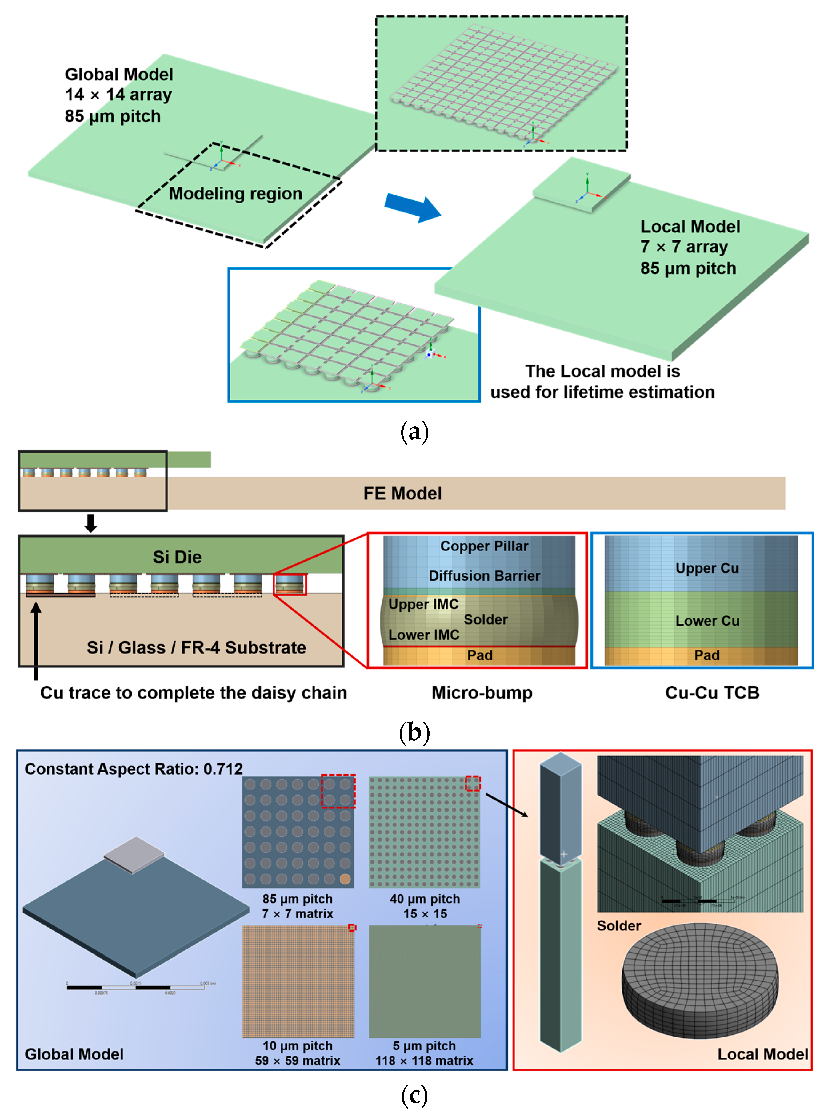
Figure 1. (a) Geometry structure of global and local model; (b) main view of local model, and magnified view of the Cu-microbump and Cu-Cu TCB structure; (c) global-local finite element modeling.
Electronicmat 06 00018 g001
Figure 2. Failure interfaces of critical interconnects: Cu-microbump with various solder materials (SAC105, Sn42Bi58, Sn63Pb37, Pb95Sn5, and Indium), and Cu-Cu TCB.
Electronicmat 06 00018 g002
Figure 3. Thermal cycling effect on (a) von Mises stress; (b) equivalent plastic strain, and (c) strain energy density in the critical microbump during the sixth thermal cycle.
Electronicmat 06 00018 g003
Figure 4. Lifetime prediction based on Engelmaier and Darveaux fatigue models.
Electronicmat 06 00018 g004
Figure 5. (a) Comparison of total and y-directional deformation in Pb95Sn5-based microbump and Cu-Cu TCB structures during the sixth thermal cycle; (b) Total deformation distribution; and (c) evolution of maximum equivalent stress in the critical microbump under three substrate configurations (Si, glass, and FR-4 substrate).
Electronicmat 06 00018 g005
Figure 6. Lifetime prediction of Pb95Sn5 and Cu-Cu TCB structures under substrate effects using the Engelmaier, Darveaux, and Coffin-Manson models (Die in all cases is silicon).
Electronicmat 06 00018 g006
Figure 7. Temperature distribution across different substrates with various solder materials, along with detailed distributions of temperature, heat flux, and temperature gradient for three substrate configurations: (a,d) Si substrate, (b,e) glass substrate, and (c,f) FR-4 substrate.
Electronicmat 06 00018 g007aElectronicmat 06 00018 g007b
Table 1. Geometric and material properties used in the FEA model.
ComponentsDimensions
(μm)
MaterialDensity
(Kg/m3)
Young’s Modulus
(E/GPa)
Poisson’s Ratio
(μ)
Coefficient of
Thermal
Expansion
a/(10−6 °C−1)
Thermal Conductivity
(W·m−1·°C−1)
Ref
Chip2000 × 1750 × 75Si23001100.242.6147[34,38]
Trace/
Pillar/
Pad
H = 4
Φ = 55, H = 15
Φ = 55, H = 5.15
Cu88891290.3417400[34,39]
Diffusion BarrierΦ = 55, H = 2Ni89022100.31213.191[40]
Solder 1Φ = 55, H = 15SAC1057400370.352060[41]
Solder 2Sn63Pb378400560.323.651[34]
Solder3Sn42Bi588700440.331517[35,42]
Solder 4Pb95Sn511,23615.70.4428.932[36,43]
Solder 5Indium7290110.453281.6[19]
IMC 1/Cu6Sn583001400.318.334.1[44,45]
IMC 2Cu3Sn89001340.331970.4[40]
IMC 3Cu11In9845090.40.3112430[46]
Substrate 17000 × 7000 × 150Si23001100.242.6147[34,38]
Substrate 2Glass2480740.239.81[47,48]
Substrate 3Organic1910220.2818.50.3[49,50]
Table 2. Kinetic parameters of IMC growth and thickness calculations.
Solder TypeIMC TypeD (m2/s)Q (KJ/mol)T (Kelvin)IMC Thickness (μm)Ref
SAC105Cu6Sn53.50 × 10−1910.4373.151.32[64]
Sn63Pb37Cu6Sn52.50 × 10−1979.8373.151.12[63]
Sn42Bi58Cu3Sn1.84 × 10−1963.5373.151[70]
Pb95Sn5Cu3Sn1.84 × 10−1952373.150.96[62]
IndiumCu11In96.45 × 10−1834.16373.155.65[65]
Table 3. Correlation constants of Darveaux constitutive model.
SolderK1 (Cycles/PsiK2)K2 (−)K3 (10−7 in/Cycles/PsiK4)K4 (−)Ref
SAC Solder40,300−1.664.261.04[75]
Lead-based eutectic solder56,300−1.623.341.04[76]
High-lead Solder71,000−1.622.761.05[77]
/K1 (cycles/PaK2)K2 (−)K3 (μm/cycles PsiK4)K4 (−)/
Indium Solder2.4 × 1011−1.370.17 × 10−50.875[78]
Table 4. Pitch effect on lifetime prediction for Cu-microbump and Cu-Cu TCB structure.
Interconnect Pitch85 μm Pitch40 μm Pitch10 μm Pitch5 μm Pitch
EngelmaierDarveauxEngelmaierDarveauxEngelmaierDarveauxEngelmaierDarveaux
SAC10532010319748733291
Indium178321712547227561822
Sn42Bi582014/1609/342/194/
Sn63Pb3728593681764123391143139
Pb95Sn53267452257114613425285820
85 μm pitch40 μm pitch10 μm pitch5 μm pitch
Coffin–MansonCoffin–MansonCoffin–MansonCoffin–Manson
Cu-Cu TCB7797526025132136
Disclaimer/Publisher’s Note: The statements, opinions and data contained in all publications are solely those of the individual author(s) and contributor(s) and not of MDPI and/or the editor(s). MDPI and/or the editor(s) disclaim responsibility for any injury to people or property resulting from any ideas, methods, instructions or products referred to in the content.