Abstract
The rising demand for increased integration and higher power outputs poses a hidden risk to the long-term reliable operation of third-generation semiconductors. Thus, the power cycling test (PCT) is widely regarded as the utmost critical test for assessing the packaging reliability of power devices. In this work, low-thermal-resistance packaging design structures of SiC devices are introduced, encompassing planar packaging with dual heat dissipation, press-pack packaging, three-dimensional (3D) packaging, and hybrid packaging. PCT methods and their control strategies are summarized and discussed. Direct-current PCT is the focus of this review. The failure mechanisms of SiC devices under PCT are pointed out. The electrical and temperature-sensitive parameters adopted to monitor the aging of SiC devices are organized. The existing international standards for PCT are evaluated. Due to the lack of authoritative statements for SiC devices, it is difficult to achieve comparison research results without consistent preconditions. Furthermore, the lifetimes of the various packaging designs of the tested SiC devices under PCTs are statistically analyzed. Additionally, problems related to parameter monitoring and test equipment are also summarized. This review explores the broader landscape by delving into the current challenges and main trends in PCTs for SiC devices.
1. Introduction
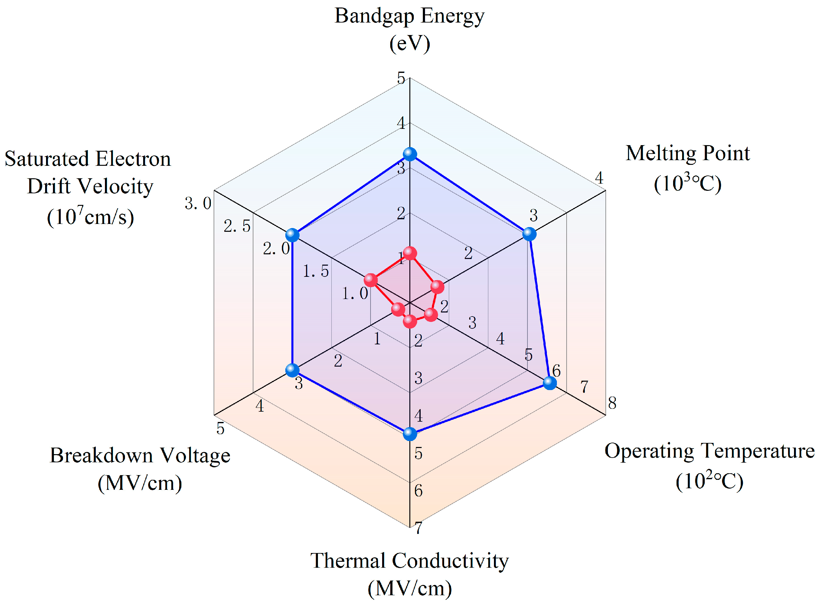
Semiconductor technology serves as the backbone of power electronics for power conversion and control [1,2]. In recent years, the paradigm shifts towards electric vehicles in transportation and the increasing development of high-efficiency photovoltaic and wind power systems in the new energy sector have highlighted the urgent need for reliable power devices that can withstand high temperatures, high power levels, and high frequencies in complex environments [3,4]. The third-generation wide-bandgap (WBG) semiconductor materials represented by SiC offer enhanced device operation at high temperatures and voltage scenarios through their lower intrinsic carrier concentration, higher breakdown electric field, superior thermal conductivity, and greater saturation electron drift speed [5,6], compared to other models, as shown in Figure 1. Si-based diodes, insulated gate bipolar transistors (IGBTs), and metal-oxide-semiconductor field-effect transistors (MOSFETs) are gradually being replaced by SiC devices, allowing for quick and cost-effective upgrades to modules and power electronic systems [7]. However, the high stiffness of SiC, with a Young modulus 3 times that of Si, leads to increased stress near the die-bonding layer [8].
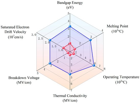
Figure 1.
Comparison of SiC and Si intrinsic properties.
Packaging, which facilitates electrical and mechanical connections, offers support and protection, provides thermal pathways, and plays a pivotal role in maximizing the performance of power devices [9]. Therefore, researchers and manufacturers have long been focused on enhancing thermal performance, interconnection processes, and attachment materials and achieving the accurate life assessment of power devices under certain operating conditions while ensuring that the failure mechanisms remain unchanged [10,11]. As a result, the long-term reliability of packaged devices has become a key focus area in the field of materials and power electronics. The operational lifetime demands for power devices to ensure a reliable performance can extend to several decades in practical working conditions [12].
PCT, a critical method for evaluating power devices, simulates the actual operating conditions by actively heating the device under test (DUT) through the application of a load current. By alternating the current’s on and off states, DUT undergoes heating and cooling cycles, leading to a junction temperature swing ΔTvj. Mismatch in the coefficients of thermal expansion (CTE) between the structural layers’ characteristics, such as “stack”, can trigger device failures [13]. Exposing the potential risk of failure caused by an inconsistent CTE in different packaging material components is regarded as the main purpose of PCT. Projects LESIT in Switzerland [14] and RAPSDRA [15] in the UK firstly emphasized the significance of PCT in assessing power device reliability and failure mechanisms. These initiatives have conducted PCTs on power devices and evaluated bonding wires and joining layers under varied load-switching conditions—ton ≤ 3 s and ton ≥ 60 s—which can be considered the earliest attempt of the two test methods illustrated in the standard. Furthermore, the power cycling life model attempted to establish incorporating the maximum junction temperature Tvjmax and a junction temperature swing ΔTvj.
To ensure consistency and reduce the disputes arising from variations in failure mechanisms, testing methods, and parameter settings, international standards such as IEC60749-34 [16], AEC-Q101 [17], AQG324 [18], JESD22-A105C [19], and JESD22-A122A [20] all provide guidelines for PCT. However, a complete and detailed authoritative description is not yet available for SiC devices. These standards establish criteria for determining device failure based on changes in on-state voltage drop and thermal resistance. The setting of the initial values is crucial and typically ranges between 5 and 100 sampling points to avoid the impact of the initial on-state electrical noise on the test outcomes. In practical working conditions, failures in SiC devices often stem from bonding wire fatigue, joining layer fatigue, and die degradation. PCT is classified into second-level and minute-level methods based on the load-switching time, allowing for reliability evaluations near and far from the source end for external packaging evaluations [16,18].
This work provides a comprehensive review of package design and PCT for SiC devices. A low-thermal-resistance package structure design that matches SiC with excellent properties is exhibited in Section 2. Then, PCT methods with their control strategies, current PCT standards, and failure behaviors under PCTs are summarized in Section 3. In Section 4, the cycling lifetimes of SiC devices with different setting conditions under PCT are counted and analyzed. Additionally, research progress and issues of PCT for SiC devices are highlighted. By reviewing the research status and challenges faced in SiC device PCTs over the past decade, this work elucidates key trends in developing SiC device’s power cycling reliability assessments.
2. SiC Power Device Package Design
2.1. SiC Device with Traditional Packaging Structures and Challenges
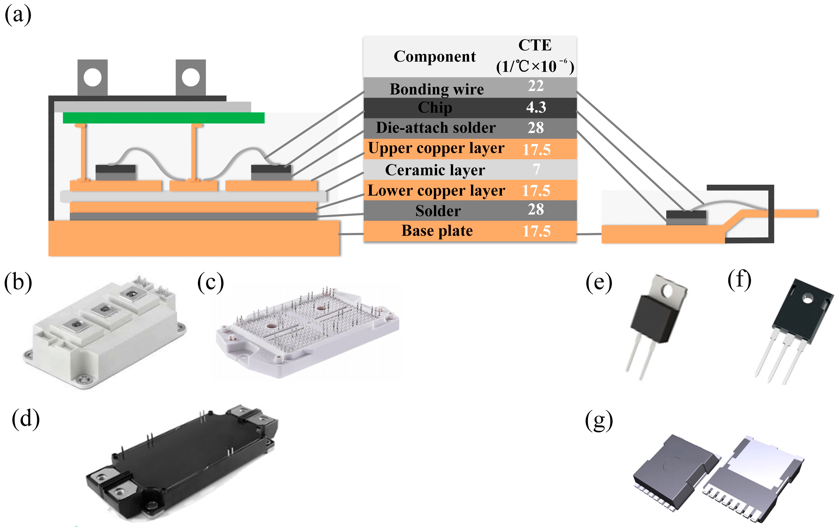
Currently, SiC devices’ manufacturing technology has matured and is being commercialized, replacing Si-based power devices in Tesla Model S and Model X [12]. Most commercial SiC power devices still adhere to the flat-packaging method of Si-based devices. As shown in Figure 2, a conventional power device is depicted where dies are mounted on the substrate using selected die attachment technology and electrical connections formed using bonding wires. However, thermal stress caused by the mismatch of CTE can damage the bonding structure, resulting in the failure of the power module. Traditional materials and processes have become a limiting factor in unleashing the full potential of SiC performance [21]. Figure 1 compares the key physical characteristics of Si and SiC. SiC exhibits excellent thermal conductivity and chemical stability under high-temperature and high-pressure operating conditions, making it an ideal material choice for maintaining high performance and stability in harsh environments.

Figure 2.
Typical power device packaging design and commercial SiC power device packages. (a) Cross-sectional view of DUT packages. (b) Semikron-1200V SiC MOSFET module—SKM500MB120SC. (c) Infineon EasyPACKTM 1200V SiC MOSFET module—FF2MR12W3M1H_B11. (d) ROHM 1200V SiC MOSFET module—BSM600D12P4G103. (e) ROHM 650V SiC Schottky diode—SCS320AH. (f) Infineon 1200V SiC Schottky diode—IDW30S120. (g) Infineon 650V SiC MOSFET—IMT65R022M1H.
The advantages of SiC are widely discussed in the current paper. However, the large Young modulus, which is about three times that of Si, poses a long-term reliability concern due to the thermal-mechanical stresses generated during the junction temperature swing ΔTvj. Herold conducted an evaluation of SiC devices through PCTs and found that they exhibited significant advantages in their electrical parameters. Nevertheless, due to their larger Young modulus and small, thin size characteristics, the plastic strain within the joining layer increased by 41%, combined with finite element analysis (FEA). Under the same packaging forms and test conditions, the reliability of SiC devices is three to four times lower than that of Si devices [22]. Similarly, there have been reports indicating that the power cycling life of SiC devices based on conventional packaging designs is merely 1/3 of that of Si-based devices [23]. In a study by Yasui, the power cycling life of SiC MOSFET and Si-diode single devices using traditional lead-rich solder was compared, revealing that the lifespan of SiC MOSFET was 2–3 times lower than that of Si-diode [24]. Therefore, developing new packaging designs to replace traditional solutions is essential to fully unleash the performance advantages of SiC devices.
Fortunately, numerous high-temperature-resistant joining materials and processes are being developed, along with new electrical interconnection materials and forms designed to align with the demanding operational environments of SiC devices. Furthermore, a packaging structure with a low thermal resistance enhances the heat dissipation capability, fully utilizes the bottom and top surface area of SiC, shortens the heat transfer path, and can significantly improve thermal management.
2.2. SiC Power Device with a Low-Thermal-Resistance Package Design
High-thermal-conductivity planar packaging, press-pack packaging, three-dimensional (3D) packaging, and hybrid packaging technologies are proposed as a trend towards the commercialization of high-reliability, high-density, and cost-effective SiC devices. The dual-sided cooling planar interconnection scheme offers enhanced thermal management and improved reliability for SiC devices without bonding wire. Woo et al. have developed a miniaturized dual-sided cooling planar packaging plan for high-power SiC inverters, which can operate at temperatures above 220 °C. As shown in Figure 3a, flip chip bonding, silver sintering, and copper clip technologies are effectively reducing the overall thermal resistance. The packaging’s thermal resistance is 0.183 K/W, only half of the traditional single-sided heat dissipation device packaging’s thermal resistance of 0.3–0.4 K/W [25]. Furthermore, a notable example is General Electric’s well-known power overlay kilowatt (POL-kW) module, which adopts a stacked planar interconnection packaging design for kilowatt-level SiC devices, exhibited in Figure 3b. Die-top interconnection is achieved through copper vias, and two active metal brazed substrates (AMB) with integrated microchannels are connected on both sides of the chip, enhancing cooling efficiency. Compared to single-sided designs, thermal resistance is reduced by approximately 50% [26,27]. Low-temperature co-fired ceramic (LTCC), an interconnection scheme for SiC devices with dual-sided cooling capabilities without bonding wires, is proposed by Zhang. The LTCC substrate, filled with high-temperature dielectric material, functions as the die carrier, with the top and bottom of the die joining to DBC using nano-silver, as shown in Figure 3c. FEAs demonstrate that the average junction temperature decreases by 32.3% compared to embedded packaging (EP) [28].

Figure 3.
Planar packaging with dual heat dissipation. (a) Miniaturized double-side cooling planar packaging based on Cu Clip interconnection. (b) Wire-bondless planar packaging module with double-side cooling. (c) LTCC-based double-side cooling planar packaging.
Press-pack packaging eliminates traditional bonding points and surfaces in packaging structures, offering a highly modular solution with a well-designed topology, which is considered a superior approach. Han evaluated the thermal characteristic parameters of high-voltage SiC devices fabricated using a press-pack packaging method that replaces wire bonding and joining, as shown in Figure 4a., The contact thermal resistances of SiC IGBT and SiC MOSFET measured by the structure function approach were only 0.6 K/W and 0.3 K/W, respectively. The thermal resistance deviation is a non-packaging factor, caused by differences in the die dimensions [29]. Gonzalez replaced the classic intermediate contact material molybdenum (Mo) with aluminum graphite (ALG), as shown in Figure 4b, and evaluated SiC devices using PCTs combined with the structure function method. Under a contact pressure of 500 N, and undergoing the same aging excitation, the thermal resistance increment in ALG contact compared to the Mo contact was reduced by 0.339 K/W, allowing the ALG device to operate at lower temperatures under the same power conditions, providing advantages for high-power-density applications [30,31]. Zhu innovatively introduced “Fuzz Button” micro-flexible pressure pads into the press-pack packaging method and combined them with a dual-sided cooling design, integrating a thin liquid-cooled heatsink with an integrated microchannel for high-power operation challenges, as shown in Figure 4c. FEAs demonstrate that the maximum junction temperature is only 85 °C, with a total dissipated power of 60 W [32].

Figure 4.
Press-pack packaging with dual heat dissipation. (a) Sandwiched configuration press-pack packaging. (b) ALG-based press-pack packaging. (c) Fuzz Button-based flexible press-pack packaging.
3D packaging effectively minimizes size and provides low-thermal-resistance packaging solutions, enhancing thermal management and system integration. As shown in Figure 5a, Fuji Electric has developed a copper pin interconnection structure to replace traditional wire bonding, combined with a silver-sintering process, significantly reducing the overall thermal resistance of SiC devices. Compared to traditional Si-based wire bonding interconnections, the overall thermal resistance is reduced by 50%, and the losses are decreased by 57–87% [33]. Mouawad, considering compact paths and effective heat management under a high power density, has proposed a highly integrated planar multi-chip 10 kV SiC MOSFET design based on stacked substrates and embedded technology, offering a strong packaging flexibility, as shown in Figure 5b. Combined with a jet-cooling design, this structure achieves junction to environmental thermal resistance of only 0.38 K/W [34]. ORNL innovatively combined genetic algorithms and 3D printing technology for optimizing a power device heatsink design and proposed a novel packaging structure for air-cooled power level 1.7 kV SiC power modules. As shown in Figure 5c, by directly connecting the device phase leg to the air-cooling component, the heat dissipation efficiency is significantly improved. The highest temperature of the semiconductor SiC bare die is only 103 °C, with the temperature variation among the MOSFETs staying within 10% under a load of 100 A and an operation above 20 kHz [35].

Figure 5.
3D packaging. (a) Cu pin interconnection-based 3D wiring packaging. (b) Wire bondless highly integrated 3D packaging with stacked substrates. (c) 3D printing technology-based air-cooled 3D packaging.
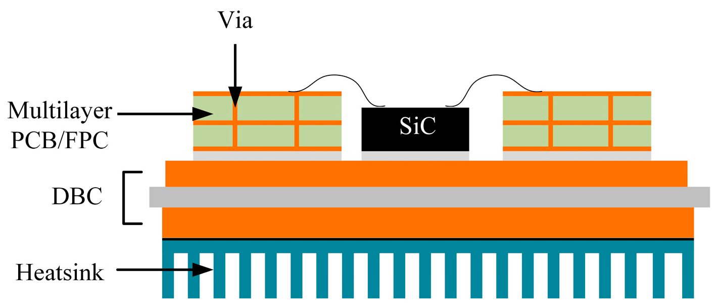
Hybrid packaging is a cost-effective strategy that significantly improves device integration and thermal management performance, while also having a lower technical complexity. Based on the DBC and the printed circuit board (PCB) hybrid packaging scheme, as well as the DBC and the flexible printed circuit (FPC) hybrid structure, there are two main hybrid packaging interconnection technologies, as shown in Figure 6. Chen has proposed connecting multi-layer grooved PCB on the DBC substrate, where SiC devices are mounted in the grooves and attached to the DBC substrate. Mature wire bonding technology is adopted to connect the top electrode of SiC with the top copper layer of the PCB [36]. The reasonably designed FPC passes through opposite currents, and this magnetic coupling response significantly reduces the parasitic inductance of the module to 0.79 nH. Furthermore, under the same driving conditions, compared to commercial modules, the switching energy loss is reduced by 1/3. This design also effectively mitigates the issue of voltage overcharge in the hybrid packaging structure, reducing it by up to 50% [37].

Figure 6.
DBC and PCB/FPC-based hybrid packaging.
3. Power Cycling Test Technology and Failure Behavior for SiC Device
3.1. Power Cycling Test Method
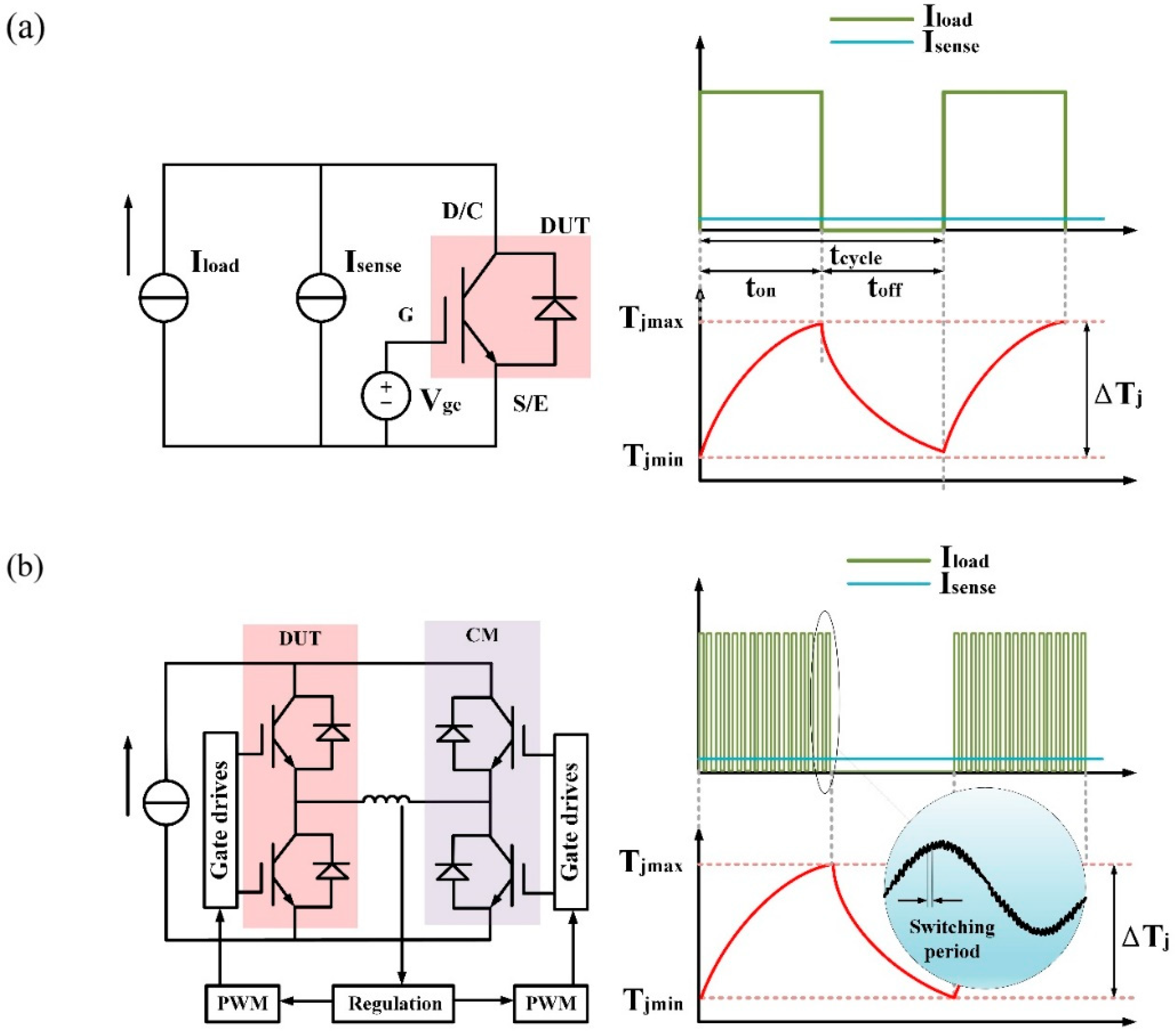
PCT can be categorized into direct-current power cycling test (DC-PCT) and pulse-width modulation power cycling test (PWM-PCT) based on variances in the current waveform input to the DUT, as shown in Figure 7. Some researchers argue that PWM-PCT is more representative of the actual operating conditions of the DUT compared to DC-PCT, as the gate control module endures frequent switching loss during transitions and high voltage levels upon deactivation [38,39]. However, there is no significant distinction in the failure modes or lifespan of the DUT between DC-PCT and PWM-PCT. The losses incurred in PWM-PCT can be addressed through thermal compensation via DC-PCT. Therefore, the reliability testing outcomes and longevity predictions derived from DC-PCT remain dependable. Moreover, DC-PCT is widely acknowledged and characterized in the industry standards. This article will concentrate on exploring DC-PCT.
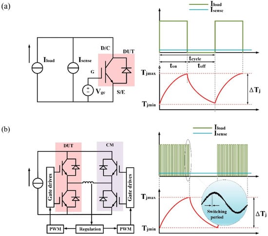
Figure 7.
Schematic diagrams of DC-PC and PWM-PCT. (a) Schematic and waveform diagrams of DC-PCT. (b) Schematic and waveform diagrams of DC-PCT.
During the conducting state, the voltage drop across the drain and source terminals of the DUT (Vds) and the thermal resistance from the junction to the substrate Rth are pivotal monitoring parameters in PCTs. These two parameters are widely regarded as indicators that can accurately reflect the aging status of DUT. However, there are controversies regarding the AQG standard definitions of failure based on a 5% increase in Vds, which is monitored in the moment before the load cutoff, and a 20% increase in Rth. These incremental monitoring parameters often combine the aging of the package and the SiC defect. Furthermore, due to the positive temperature-sensitive characteristics of DUT, the degradation effects of packaging intensify the on-state losses and ΔTvj, significantly accelerating the failure process through positive feedback loops. Therefore, the response of DUT to degradation is crucial during PCTs, and the setting of control strategies before testing is closely linked to the lifetime characteristics of DUT.
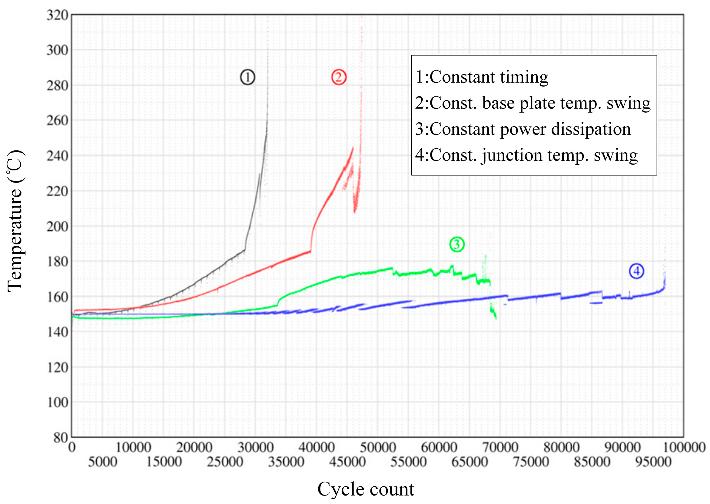
Based on the evaluation strictness level of DUT, the test strategy order from high to low is as follows: constant conduction time (Δton), constant case temperature swing (ΔTc), constant power loss (ΔP), and constant junction temperature swing (ΔTvj), as shown in Figure 8. The Δton control strategy is considered the most rigorous approach. Studies have revealed that the ΔTc control strategy compensates for the degradation of interface performance between the tested device and the heat dissipation structure by establishing a feedback relationship between the case temperature and the cooling medium’s temperature, resulting in a lifespan which is approximately 1.5 times longer than the Δton control strategy [40]. The ΔP control strategy is often combined with the Δton strategy, utilizing load current and gate voltage regulation to offset the increase in power loss due to the aging of DUT, resulting in a lifespan approximately 2 times as long as the standard test method [40]. The ΔTvj control strategy maintains the junction temperature swing of DUT through the synchronous regulation of load current, conduction on/off time, and gate voltage, with a constant aging stimulus source. Compared to the standard method, the lifespan is approximately 3 times longer than Δton [40].
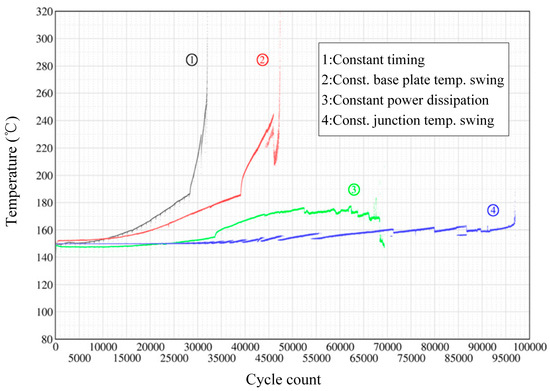
Figure 8.
Power cycling test with four different control strategies [40].
3.2. SiC Device’s Failure Behavior under the Power Cycling Test
The failure modes of SiC power devices can be divided into failures at the chip level and failures at the packaging level. Gate oxide degradation is the most significant reliability issue in PCTs at the chip level, mainly due to the high density of interface traps at the SiC/SiO2 interface [41]. WBG, combined with the small bandgap between the semiconductor material and the oxide layer, makes it easy for electrons to transition to the oxide layer, increasing the risk of gate–source short circuits [42]. Additionally, the thin gate oxide layer design increases the risk of failure under high-power applications of SiC devices [43].
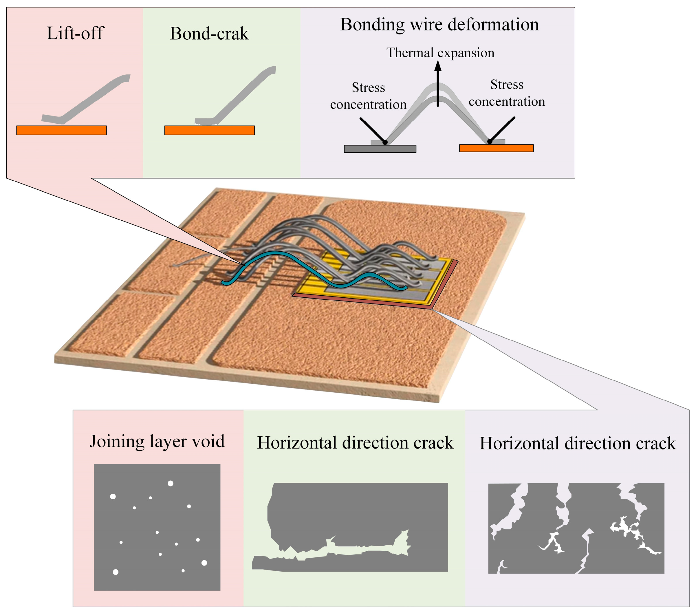
On the other hand, most SiC power devices adopt the packaging structure design for Si power devices. Therefore, the thermal-mechanical stress caused by a mismatch in the CTE between the stacked layers of materials is also a major reason for SiC device packaging failure. Prolonged cyclic thermal stress can lead to the bending, cracking, or even detachment of bond wires [44]. SiC devices’ typical failure mechanisms under PCT are shown in Figure 9. Under positive feedback, the aging of bond wires can lead to an increase in bond wire resistance, resulting in increased power consumption and causing further elevation of the junction temperature Tvjmax and the junction temperature swing ΔTvj, thus accelerating the aging of the DUT. Reference [45] measured the displacement of bond wires after thermal expansion, showing that the arcuate displacement of the bond wire was approximately 16 μm under a current of 50 A. Additionally, the formation of delamination, cracks, and voids in the joining layers can increase the thermal resistance of the device, causing further increases in the junction temperature Tvjmax and the junction temperature swing ΔTvj, which also accelerate device failure [46]. The degradation of the joining layer in PCTs is tightly related to factor ton. Furthermore, phenomena such as the ratcheting effect on the die-top metallization layer, substrate delamination, and cracking have been also observed in PCT. However, bond wires and joining layers are typically the two most vulnerable areas for failure in the packaging structure of power devices [47], underscoring the need to monitor the aging status of bond wires and joining layers during the PCT process.

Figure 9.
SiC device’s typical failure mechanisms under the power cycling test.
3.3. SiC Device Power Cycling Test’s Monitoring Method
Monitoring the aging-sensitive parameters of SiC devices in PCTs can achieve online status awareness and feedback on packaging defects of DUT. Currently, even commercialized SiC devices lack comprehensive aging records of PCT; therefore, it is crucial to select appropriate precursor parameters for aging before improving reliability assessments. The main monitoring parameters are electrical signals and thermal parameters as follows.
Electrical signals are commonly utilized to assess the electrical interconnection status, with wire bonding failure being a frequent issue in power devices which can result in internal electrical connection breakages. The status of wire bonding can be monitored by observing the static parameter Vds, which represents the voltage drop between the drain and the source. An increase in Vds signifies bonding wire degradation, while a sudden change indicates bond wire detachment failure [48]. On-state resistance (Ron) is the selected bonding wire aging characteristic parameter in standard AQG324. However, the drift in threshold voltage during the aging process of SiC devices also causes an increase in chip resistance, which, in turn, leads to an increase in Ron. As a result, Ron is not suitable in this case. Additionally, changes in dynamic parameters like gate voltage overshoot [49], collector voltage overshoot, and oscillations during the turn-off process [50], as well as collector voltage undershoot of bridge arm devices during turn-off, can also be considered as indicators of the wire bonding status [51]. Variations in the magnetic field resulting from sudden current transients during turn-on and turn-off moments can also serve as monitoring parameters, including alterations in the magnetic induction strength [52] and spectral characteristics [53]. The gate charging charge [54] and the gate charging time [55] have been explored as signals for detecting the wire bonding status in multi-chip parallel modules. When all wire bonds within a parallel branch are disconnected, there is a change in the input capacitance of the parallel chip.
The degradation of the joining layer in packaged devices typically coincides with an increase in thermal resistance Rth, junction temperature Tvjmax, case temperature Tc, and load current Iload. The junction temperature serves as the foundation for thermal resistance calculations:
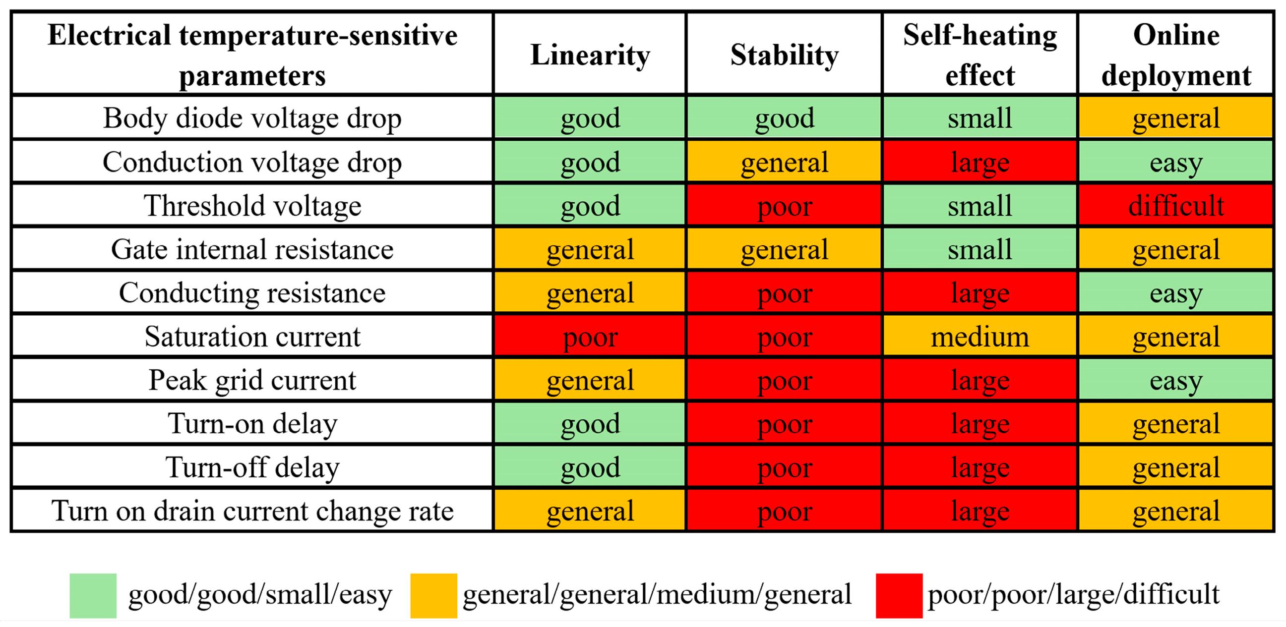
Thus, detecting the junction temperature can offer insights into the status of the joining layer. The temperature-sensitive parameter method, a non-destructive temperature measurement approach known for its rapid response and non-destructive nature, has been extensively explored by researchers. These temperature-sensitive parameters are utilized to track junction temperature changes in PCTs. Body diode voltage drop [56], conduction voltage drop [57], threshold voltage [58], gate internal resistance [59], conduction resistance [60], saturation current [61], peak grid current [62], turn-on delay [63], turn-off delay [64], and leakage current during conduction transients [65] are existing electrical temperature-sensitive parameters of SiC devices that have been studied, playing a crucial role in assessing thermal characteristics. The electroluminescence effect of SiC devices has also been investigated for the real-time detection of junction temperature [66]. Additionally, data-driven techniques based on thermal-sensitive parameters’ data are commonly employed for monitoring the condition of joining layers [67]. Figure 10 summarizes the existing electrical method’s temperature-sensitive parameters of SiC devices with the consideration of measurement effectiveness and online implementation difficulty. The methods mentioned above, such as the threshold voltage, the on-state voltage drop, and the resistance, demonstrate good versatility but are prone to couple the effects of bond wire aging [57,58,60]. The saturation current method requires a modification in the control strategy of the device, which will impacting the operational conditions [61]. The approaches based on gate parameters are susceptible to the noise interference caused by parasitic parameters within the system during the high-frequency operation of devices [59,62]. Time–temperature-sensitive parameters are limited by sensitivity and necessitate a high-resolution timer [63,64]. Similarly, detecting the di/dt of the switch-on process presents a deployment cost issue [65]. For SiC devices with an inherent diode, effectively reflecting the device junction temperature can be achieved by observing the on-state voltage drop of the diode during device turn-off [56]. Certainly, different temperature-sensitive parameter extraction methods have distinct characteristics, so the specific parameter selection should be based on the actual operating conditions and measurement requirements.
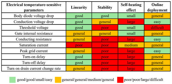
Figure 10.
Comparison of electrical temperature-sensitive parameters of SiC devices [56,57,58,59,60,61,62,63,64,65].
However, the presence of interface traps in SiC can easily cause electrical parameter drift. Currently, ongoing research is focusing on minimizing the impact of traps as much as possible and achieving more accurate junction temperature measurements. Furthermore, in the field of thermal resistance analysis, the transient dual-interface thermal resistance method and the structural function analysis method have been developed to measure the degradation of thermal resistance in a single-layer structure, especially for the joining layer [68].
3.4. Power Cycling Test Standards’ Discussion
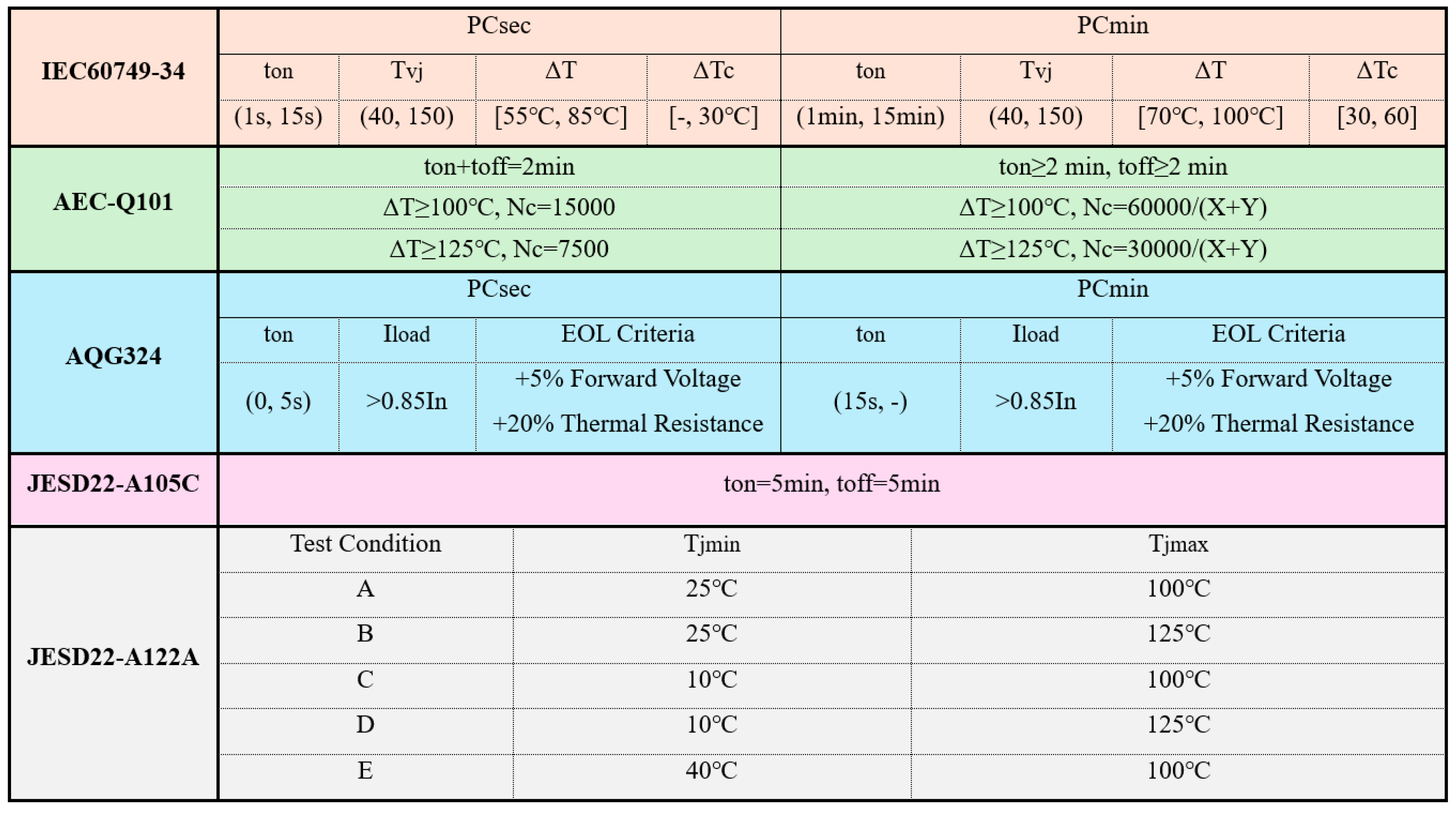
PCT standards have been developed to standardize testing conditions and measure the reliability of DUT within a uniform framework, thus improving the comparability of reliability within the same device iteration and between devices of the same type, promoting interoperability and the mutual recognition of device performance. Five standards for PCT settings are illustrated in Figure 11. According to IEC 60749-34, PCTs have been divided based on their failure behavior. Failures sensitive to wire bonding are conducted at the second level—1 s < ton < 15 s—while tests sensitive to the joining layer and wire bonding failures are conducted at the minute level, 1 min < ton < 15 min. There is no defined minimum requirement for the number of cycles, as it is considered to depend on specific application scenarios. For example, in the traction field, millions of cycles may be required. Additionally, the standard provides reference values for the junction temperature Tvj, the junction temperature swing ΔTvj, and the case temperature swing ΔTc [16]. The release of AEC-Q101 is a reliability test setting for semiconductor discrete devices. The PCT section defines the exact number of cycles, as shown in Figure 11. Similarly, the classification of the two test conditions is also based on the failure behavior of DUT, the setting of on/off times, and the junction temperature swing ΔTvj [17]. AQG324 is a standard specifically aimed at power devices for electric vehicles, published by the European Power Electronics Center. This standard focuses on the failure behavior of DUT, utilizing monitored parameters of electrical and thermal degradation to determine the cutoff criteria number of cycle, but it does not specify a minimum number of required cycles. Similar to IEC60749-34, PCTs at the second level ton < 5 s primarily address the reliability of interconnections around the die, while PCTs at the minute level ton > 15s mainly assess reliability further away from the die connections [18]. JESD22-A105C only defines the turn-on and turn-off times and the load current, and it does not specify specific requirements for other test settings [19]. JESD22-A122A is an industry PCT method for solid-state device packages. The standard explains two types of test settings: constant power and variable power. It provides typical power cycling evaluation test conditions, only defines the test temperature settings, and does not provide any other test settings or test cutoff criteria [20].
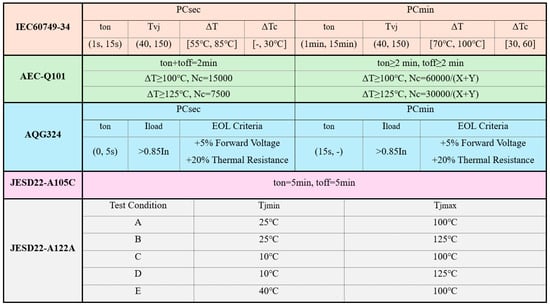
Figure 11.
Power cycling test standard summary [16,17,18,19,20].
In conclusion, the existing testing standards have been developed based on the reliability testing standards for Si-based power devices. The focus of these tests varies, and the test settings are not standardized. Different definitions are provided for the setting of the key setting parameter ton in IEC60749-34, AEC-Q101, AQG324, and JESD22-A105C. Additionally, there is inconsistency in the descriptions of the cutoff for the PCT cycle counts. Particularly, as the current standards do not provide specific guidelines for PCTs on SiC devices, the testing methods and failure criteria do not consider the unique challenges associated with SiC devices. In IEC 60749-34, the thermal interface material (TIM) and the substrate are considered parts of the device and are required not to be moved during the measurement process. This poses challenges for conducting threshold voltage drift measurements on SiC devices using a two-step method. Furthermore, limitations in the measurement points and methods for the case temperature make the physical significance of the junction temperature and the temperature gradient calculated at that temperature unclear. Due to thermal resistance being a relative value which includes the contact thermal resistance and other structural thermal resistances, the reasons for device thermal impedance degradation cannot be determined. The most critical issue is, currently, the lack of a definitive standard for the PCT conditions for SiC devices, especially regarding the junction temperature swing ΔTvj and the maximum junction temperature Tvjmax. While some researchers have utilized more demanding test conditions than those for Si-based devices to showcase the superiority of SiC power devices, this approach is not universally accepted as a reference. Therefore, there is an urgent need to clarify the range of test conditions and bridge the gap in comparative research in PCTs for SiC devices. Adjusting them while ensuring the stable operation of the equipment is of great significance for saving industry resources.
4. SiC Device Power Cycling Test’s Statistics and Challenges
4.1. Research Status in SiC Device Power Cycling Tests
The engineering field has seen significant development in the production of SiC devices, including Schottky diodes, MOSFETs, JFETs, and IGBTs, which are commercially available. In Hanif and Peyghami’s research, a 10 °C increase in the mean junction temperature Tm and a 5 °C increase in the junction temperature swing ΔTvj can substantially reduce the lifespan of DUT under PCTs, potentially cutting it in half [69,70]. As mentioned above, the degradation of SiC in PCTs can result in the forward drift in the threshold voltage and an increase in the on-state resistance. Balachandran found that, in power cycling operations, the milliamp-level currents adopted for junction temperature measurements do not trigger the degradation of SiC body diodes compared to load currents. And, with the improvement of SiC’s manufacturing processes, the phenomenon of degradation and consumption due to packaging in SiC body diodes is no longer significant [71]. Another phenomenon is that, when the applied voltage drop on the gate of DUT is less than −4 V, the voltage drop generated by the test current flowing through the body diode has been proven to be a reliable temperature-sensitive parameter. Therefore, to avoid the problem of temperature-sensitive parameters being affected by packaging and causing errors in the junction temperature measurements during PCTs, the voltage drop across the body diode under a −5 V gate bias of the SiC MOSFET is typically chosen. This parameter exhibits a linear correlation with the junction temperature and is employed for the calibration of the relationship with the junction temperature [23,72].
In the monitoring of the degradation parameters during PCTs for SiC MOSFETs, monitored parameters such as the on-state resistance and the voltage drop deteriorated, coupling the effects of power cycling excitation aging and SiC defects. Additionally, immature SiC manufacturing processes in gate oxidation can also worsen DUT failures in PCTs [73,74]. Therefore, decoupling measurements of the two types of aging issues are crucial for eliminating the misjudgment of failure modes. The literature [75,76] has attempted to propose methods for decoupling testing, where Kelvin connections have been adopted to separately measure the on-state voltage drop representing the degradation of the SiC MOSFET and the bonding wire voltage drop representing the degradation of the package. In addition, with the presence of this combined degradation effect, the standard criterion of a 5% increase in the on-state voltage drop for failure detection is no longer applicable. Luo et al. proposed using a sudden change in on-state voltage drop or a 15% increase in the on-state voltage drop as the criterion for failure detection [75]. TIMs are used in PCTs to ensure tight contact between the tested device and the cold plate to enhance heat conduction. However, the aging of TIMs can also increase the junction temperature of the device and accelerate device failure [76]. Zhang et al. proposed a concept of relative Vce(on) defined as
to avoid the interference of the testing environment and TIM aging in determining the lifespan of IGBT based on Vce(on) [77]. Therefore, the PCTs for SiC devices and the improvement of SiC devices’ power cycling reliability are systematic engineering processes.
4.2. Power Cycling Test Statistics for SiC Device’s Interconnection Technology
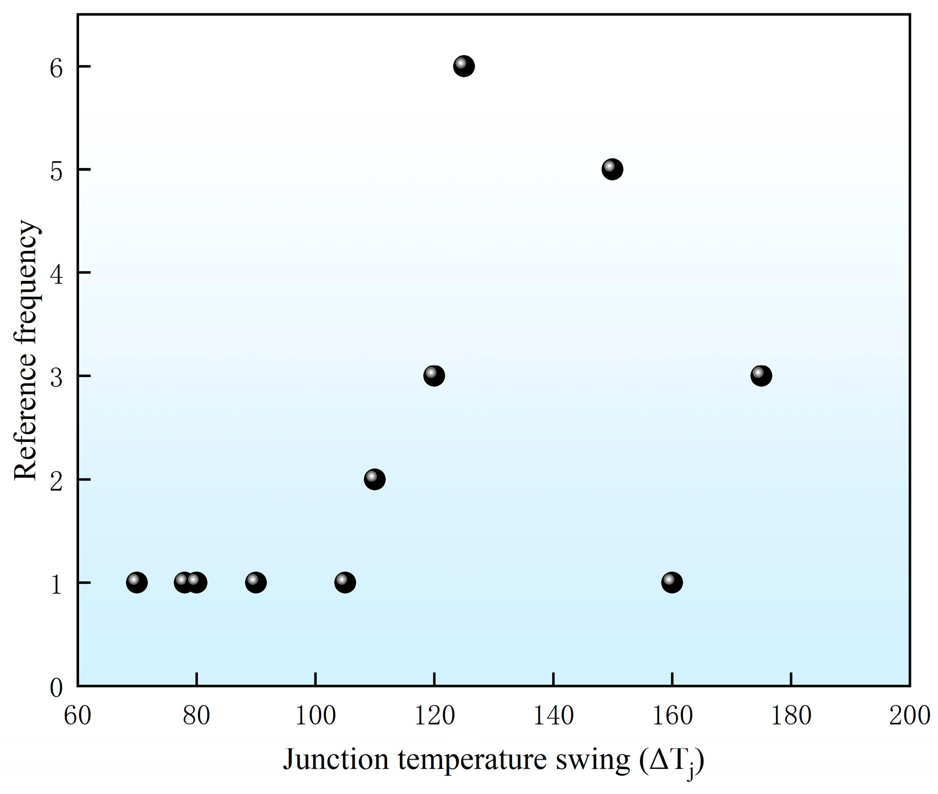
There is currently no international standard for PCTs on SiC devices. In group standards, ΔT ≥ 125 °C is typically set for SiC device’s PCTs. However, due to variations in the research objectives or points, there is inconsistency in the temperature swing ΔTvj. A statistical analysis of the operating conditions of PCTs in 25 literature sources is shown in Figure 12. Within the limited scope of SiC devices and their joining technologies, the statistical frequency of the temperature difference settings exhibits a distribution that resembles a Gaussian curve. A temperature swing range of 120 °C ≤ ΔTvj ≤ 150 °C seems to be more appropriate for SiC power devices’ PCT settings.
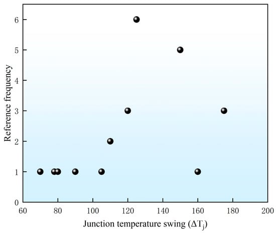
Figure 12.
Temperature swing ΔTj’ s setting frequency in studies [8,77,78,79,80,81,82,83,84,85,86,87,88,89,90,91,92,93,94,95,96,97,98].
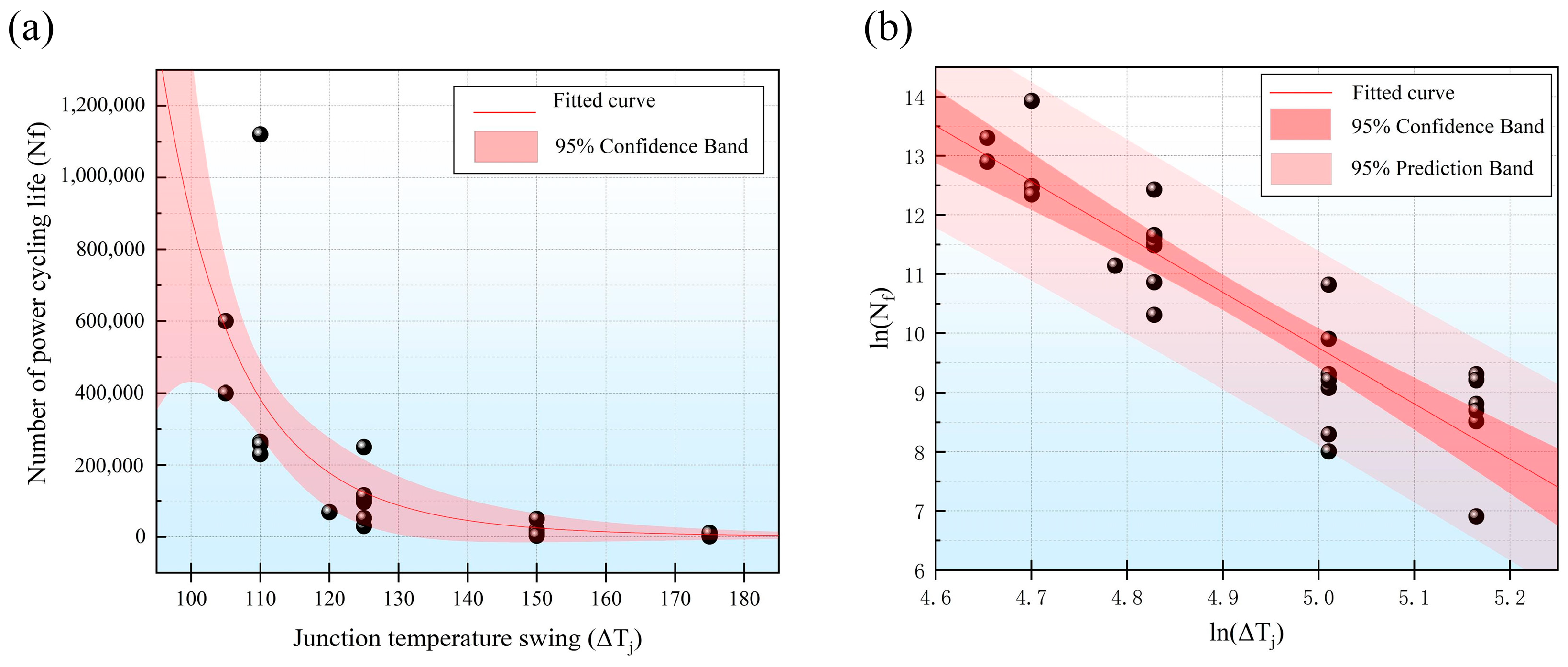
To have an overview of the impact of the temperature swing on the lifespan of SiC devices under PCTs, the relationship between the failure cycle numbers and the temperature swing from the collected literature is illustrated in Figure 13. A straightforward statistical analysis reveals a consistent inverse relationship between the cycle lifespan and the temperature swings. Furthermore, Figure 13a shows a regression analysis, revealing an exponential distribution in the fitted curve. This summary is based on a limited number of literature sources on PCT results and lacks uniform test conditions. As shown in Figure 13b, it still effectively demonstrates the correlation between the power cycling lifetime and the junction temperature swing ΔTj in the Coffin–Manson model [99], which is expressed as follows. The fitted results show that coefficients A and α are 4.2 × 10²³ and 8.8, respectively.
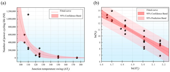
Figure 13.
Number of cycles to failure under different temperature swings ΔTvj [8,77,78,79,80,81,82,83,84,85,86,87,88,89,90,91,92,93,94,95,96,97,98]. (a) Power cycling results’ fitted curve based on the data in the references. (b) The power cycling results’ fitted curve refers to the Coffin–Manson model.
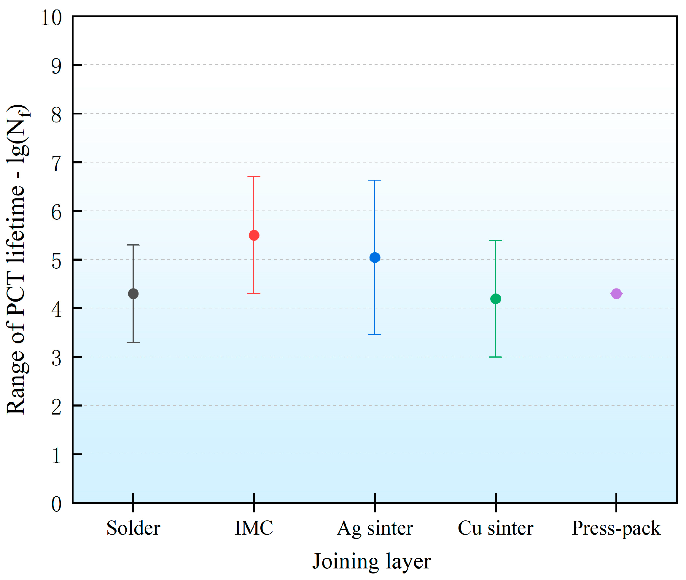
Additionally, in most publications focusing on SiC devices’ PCTs, significant attention is given to the joining layer. Despite the influence of the test conditions and the monitoring methods on the measurement outcomes, the standardization of the die-top interconnection form as a key test condition enables the statistical analysis of the PCT lifespan ranges for four different joining layers. As shown in Figure 14, the highest lifespan of 5,100,510 is achieved with the combination of the intermetallic compound (IMC) and transient liquid-phase bonding technology (TLPB) [89]. However, concerns arise from the complex and slow diffusion processes, questioning its efficiency as a packaging technology. Fortunately, the pulsed laser deposition technology, as well as other auxiliary accelerated diffusion technologies, provide the potential for rapid IMC joint preparation. Nano-silver and nano-copper are focal points in commercial packaging material research, with the statistical evidence shown in Figure 14 seemingly suggesting that nano-silver surpasses nano-copper in terms of maximum cycle lifespan. However, under unified testing conditions, nano-copper demonstrates a significant power cycling reliability. Yasui used sintered copper and sintered silver as alternative options to traditional solder paste mounting processes and conducted PCTs for evaluation [94]. Sintered copper showed more stable temperature fluctuations than sintered silver, with a lifespan 2.5 times longer than sintered silver. The cracks in sintered copper were limited to the die perimeter and did not cause thermal resistance degradation or the exacerbation of temperature fluctuation aging like thin cracks between the sintered silver device’s joining layer and the die bottom layer [94]. Therefore, effective conclusions can be drawn within a unified framework; otherwise, there will be controversy. The literature on PCTs for press-pack packaging is insufficient. While press-pack technology avoids the fatigue of joining layers under thermal cycling stress, it shows a potential in PCTs that is comparable to soldering processes. In the research conducted by Dai, as the aging process of PCTs progresses, both the on-state resistance and the contact resistance increase. The resistance between the plate and the emitter shows a linear growth trend. Additionally, the degradation of branches with an insufficient contact status is more severe compared to chips with an adequate contact status, particularly in situations with a lower clamping force and a longer heating time [98]. Therefore, contact pressure and heating time settings have a significant impact on critical contact aging parameters for press-pack packaging devices under PCTs. In addition to the information mentioned above, novel materials with significant commercial potential and comprehensive performance in the joining layer, such as multi-peak nanoparticles [100], reinforced nano paste [101], and composite nanomaterials [102,103], are being studied.
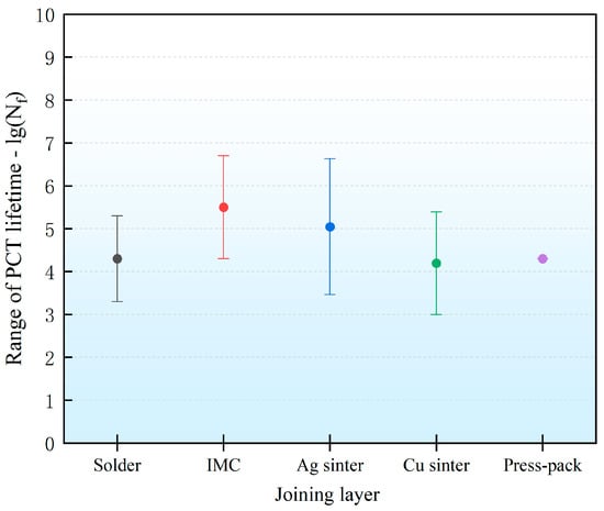
Figure 14.
Power cycling lifetime statistics with different joining layers [8,77,78,79,80,81,82,83,84,85,86,87,88,89,90,91,92,93,94,95,96,97,98].
4.3. Challenges in SiC Devices’ Design and Power Cycling Tests
To meet the demands for enhanced energy efficiency and power density in industrial settings, there is a pressing need for swift replacement with cost-effective alternatives to facilitate efficient upgrades to power devices. The issue of PCT in traditional Si-based packaging is inherited in SiC devices and fully exposed. High-power-density and thermal management challenges of SiC devices under high-temperature operations pose demands for package heat dissipation design [104]. Additionally, the high switching speed imposes requirements on layout and interconnection design. As illustrated in Figure 15, a quantitative comparison of dv/dt and di/dt for Si IGBT and SiC MOSFET devices with the same rate of power was performed. The outstanding switching frequency characteristics of SiC devices make them more susceptible to the influence of parasitic parameters [105]. On the other hand, most of the SiC currently available on the market are designed for Al wire bonding, which is incompatible with wireless interconnections in excellent heat dissipation designs. Additionally, the high cost and risks associated with the further metallization of SiC wafer-level solder pads pose a significant challenge.
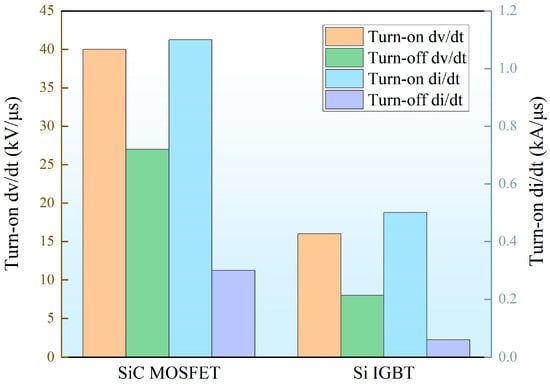
Figure 15.
Conversion speed of SiC MOSFET and Si IGBT [104].
Currently, judging the degree of packaging degradation based on the precursor parameters of the tested device before aging, such as the on-state voltage drop, the conduction resistance, etc., couples the SiC defect and packaging degradation issues. Commercial PCT platforms cannot effectively differentiate the failure behavior of the tested device caused by the two types of degradation reasons: chip and packaging. Limited by the testing methods, regarding the measurement of the threshold voltage for SiC devices, the existing research mostly adopts a two-stage offline measurement method. Since the threshold voltage drift in the device couples reversible and irreversible parts, turning off PCT and shorting the gated-source circuit eliminate the reversible drift. Therefore, only the irreversible drift can be measured, which cannot provide an effective reference for the threshold voltage changes in SiC devices under continuous operation, especially in serial application scenarios. Furthermore, TIM undergoes aging along with the PCT, as the increase in thermal resistance couples with the TIM degradation factors. Moreover, applying the TIM before testing and reinstalling it after an interruption in measurements can both change the PCT conditions, introducing test errors. The structure function method is commonly utilized to monitor variations in the thermal resistance of multilayer structures. However, due to the impact of measurement errors and noise introduced by algorithm conversion, the resulting structure function curve may contain inaccuracies. This can result in disparities between the thermal resistance values of multilayer structures derived from changes in the curve slope and the actual values. Last but not least, most of the current research on the power cycling reliability of SiC devices is limited to individual discrete devices or modules, with few scholars conducting studies using system-level modules as the test subjects. In conclusion, SiC devices inherit issues from traditional device packaging designs and PCT methods and also introduce new challenges. There exists a research gap, and addressing these issues will be a key focus of research on the reliability of SiC devices in the present and future.
5. Conclusions
This work provides a comprehensive overview of PCTs on SiC devices. PCTs have exposed the long-term stability risks of SiC devices with traditional packaging designs. Currently, a series of low-thermal-resistance packaging structure designs is being developed to accommodate a high power density. Double-sided cooling planar packaging opens a new heat dissipation path while incorporating a top interconnection design from point to surface; press-pack packaging removes the bonding structure and incorporates dual-sided heat dissipation channels; 3D packaging endows an integrated system and thermal management with flexible layout advantages; and hybrid packaging provides significant cost-effectiveness and reliability improvements. These designs are in line with the current urgent requirements of SiC devices and align well with the current market demands. Furthermore, by reviewing and analyzing the current research status of PCTs for SiC devices, it has been observed that the ΔTvj serves as a critical aging stimulus in the tests, with a focus on the temperature range of 120 to 150 °C. It has been noted that the power cycling lifetime of SiC devices demonstrates an exponential distribution with increasing ΔTvj, and the results are consistent with the Coffin–Manson model after natural logarithm processing. Additionally, the existing international standards do not specify the conditions for the PCTs of SiC devices. Researchers have not conducted studies within a unified framework to highlight the advantages of SiC devices and develop packaging schemes. Some studies have been carried out under harsh thermal settings’ conditions, resulting in relatively longer PC lifetimes, which are praised, but there is no guidance for the test settings. Moreover, blindly comparing the performance of various packaging schemes under non-uniform testing conditions may result in erroneous conclusions, causing challenges for researchers in terms of conducting comparative studies. Notably, classic pre-encapsulation aging precursors such as Vsd and Rth, which commercial testing platforms and researchers are focusing on, couple chip degradation with packaging degradation issues. Therefore, achieving a decoupling analysis of aging behavior and developing more targeted efficient PCT methods for SiC devices are also current hot topics in reliability research, while, in addition to what is mentioned in this work, both academia and the industry have generated numerous innovative designs and PCT approaches for WBG power devices. With the deepening of research on SiC devices and packaging testing, power device systems’ design and reliability assessments will be comprehensively upgraded in all aspects.
Author Contributions
Supervision, G.Z.; Resources, Project administration, F.G.; Validation, L.M.; Writing—review & editing, H.Z.; Data curation, Y.W.; Writing—original draft, Formal analysis, X.G.; Funding acquisition, Q.J. All authors have read and agreed to the published version of the manuscript.
Funding
This research was funded by [National Natural Science Foundation of China] grant number [52205324], [Chongqing Natural Science Foundation project] grant number [CSTB2023NSCQ-MSX0187], [Beijing Natural Science Foundation] grant number [L233038], [R&D Program of the Beijing Municipal Education Commission] grant number [KZ202210005005].
Data Availability Statement
The original contributions presented in the study are included in the article, further inquiries can be directed to the corresponding authors.
Conflicts of Interest
The authors declare no conflicts of interest.
References
- Chen, C.; Luo, F.; Kang, Y. A review of SiC power module packaging: Layout, material system and integration. CPSS Trans. Power Electron. Appl. 2017, 2, 170–186. [Google Scholar] [CrossRef]
- Ren, H.; Zou, G.; Jia, Q.; Deng, Z.; Du, C.; Wang, W.; Liu, L. Thermal stress reduction strategy for high-temperature power electronics with Ag sintering. Microelectron. Reliab. 2021, 127, 114379. [Google Scholar] [CrossRef]
- Castro, C.; Reiter, T.; Graovac, D.; Christmann, A. Application requirements for automotive power modules. In Proceedings of the SIA 4th International Conference and Exhibition, Paris, France, 6–7 April 2011. [Google Scholar]
- Ren, H.; Zou, G.; Zhao, Z.; Wan, M.; Zhang, H.; Jia, Q.; Liu, L. High-reliability wireless packaging for high-temperature SiC power device sintered by novel organic-free nanomaterial. IEEE Trans. Compon. Packag. Manuf. Technol. 2020, 10, 1953–1959. [Google Scholar] [CrossRef]
- Varley, J.B.; Shen, B.; Higashiwaki, M. Wide bandgap semiconductor materials and devices. J. Appl. Phys. 2022, 131, 230401. [Google Scholar] [CrossRef]
- PowerAmerica. PowerAmerica Strategic Roadmap for Next Generation Wide Bandgap Power Electronics; PowerAmerica: Raleigh, NC, USA, 2017. [Google Scholar]
- Liang, Z.; Ning, P.; Wang, F. Development of advanced all-SiC power modules. IEEE Trans. Power Electron. 2013, 29, 2289–2295. [Google Scholar] [CrossRef]
- Kovacevic-Badstuebner, I.; Race, S.; Ziemann, T.; Tiwari, S.; Grossner, U.; Mengotti, E.; Bianda, E.; Jormanainen, J. Power cycling reliability of SiC MOSFETs in discrete and module packages. In Proceedings of the International Reliability Physics Symposium, Dallas, TX, USA, 27–31 March 2022. [Google Scholar]
- Wang, L.; Wang, W.; Hueting, R.J.; Rietveld, G.; Ferreira, J. Review of topside interconnections for wide bandgap power semiconductor packaging. IEEE Trans. Power Electron. 2022, 38, 472–490. [Google Scholar] [CrossRef]
- Schmidt, R.; Scheuermann, U. Separating failure modes in power cycling tests. In Proceedings of the International Conference on Integrated Power Electronics Systems, Nuremberg, Germany, 6–8 March 2012. [Google Scholar]
- GopiReddy, L.R.; Tolbert, L.M.; Ozpineci, B. Power cycle testing of power switches: A literature survey. IEEE Trans. Power Electron. 2014, 30, 2465–2473. [Google Scholar]
- Yang, Y.; Dorn-Gomba, L.; Rodriguez, R.; Mak, C.; Emadi, A. Automotive power module packaging: Current status and future trends. IEEE Access 2020, 8, 160126–160144. [Google Scholar] [CrossRef]
- Durand, C.; Klingler, M.; Coutellier, D.; Naceur, H. Power cycling reliability of power module: A survey. IEEE Trans. Device Mater. Reliab. 2016, 16, 80–97. [Google Scholar] [CrossRef]
- Held, M.; Jacob, P.; Nicoletti, G.; Scacco, P.; Poech, M.-H. Fast power cycling test of IGBT modules in traction application. In Proceedings of the Second International Conference on Power Electronics and Drive Systems, Singapore, 26–29 May 1997. [Google Scholar]
- Berg, H.; Wolfgang, E. Advanced IGBT modules for railway traction applications: Reliability testing. Microelectron. Reliab. 1998, 38, 1319–1323. [Google Scholar] [CrossRef]
- DS/EN 60749-34-2010; Semiconductor Devices-Mechanical and Climatic Test Methods—Part 34: Power Cycling. ECPE: Nuremberg, Germany, 2010.
- Automotive Electronics Council Component Technical Committee. AEC-Q101 Failure Mechanism Based Stress Test Qualification for Discrete Semiconductors in Automative Applications; AEC: USA, 2021. [Google Scholar]
- AQG 324 Qualification of Power Modules for Use in Power Electronics Converter Units (PCUs) in Motor Vehicles; ECPE: Nuremberg, Germany, 2018.
- JESD22-A105C; Power and Temperature Cycling. JEDEC: Arlington, VA, USA, 2004.
- JESD22-A122A; Power Cycling, JEDEC Solid State Technology Association. JEDEC: Arlington, VA, USA, 2016.
- Chidambaram, V.; Hattel, J.; Hald, J. Design of lead-free candidate alloys for high-temperature soldering based on the Au–Sn system. Mater. Des. 2010, 31, 4638–4645. [Google Scholar] [CrossRef]
- Herold, C.; Schaefer, M.; Sauerland, F.; Poller, T.; Lutz, J.; Schilling, O. Power cycling capability of Modules with SiC-Diodes. In Proceedings of the 8th International Conference on Integrated Power Electronics Systems, Nuremberg, Germany, 25–27 February 2014. [Google Scholar]
- Herold, C.; Sun, J.; Seidel, P.; Tinschert, L.; Lutz, J. Power cycling methods for SiC MOSFETs. In Proceedings of the 29th International Symposium on Power Semiconductor Devices and IC’s, Sapporo, Japan, 28 May–1 June 2017. [Google Scholar]
- Yasui, K.; Hayakawa, S.; Nakamura, M.; Kawase, D.; Ishigaki, T.; Sasaki, K.; Tabata, T.; Morita, T.; Sagawa, M.; Matsushima, H. Improvement of power cycling reliability of 3.3 kV full-SiC power modules with sintered copper technology for Tjmax = 175 °C. In Proceedings of the 30th International Symposium on Power Semiconductor Devices and ICs, Chicago, IL, USA, 13–17 May 2018. [Google Scholar]
- Woo, D.R.M.; Yuan, H.H.; Li, J.A.J.; Bum, L.J.; Hengyun, Z. Miniaturized double side cooling packaging for high power 3 phase SiC inverter module with junction temperature over 220 °C. In Proceedings of the 66th Electronic Components and Technology, Las Vegas, NV, USA, 31 May–3 June 2016. [Google Scholar]
- Yin, L.; Kapusta, C.; Gowda, A.; Nagarkar, k. A wire-bondless packaging platform for silicon carbide power semiconductor devices. J. Electron. Packag. 2018, 140, 031009. [Google Scholar] [CrossRef]
- Yin, L.; Nagarkar, K.; Gowda, A.; Kapusta, C.; Tuominen, R.; Gillespie, P.; Sherman, D.; Johnson, T.; Hayashibe, S. POL-kw modules for high power applications. In Proceedings of the 67th Electronic Components and Technology Conference, Orlando, FL, USA, 30 May–2 June 2017. [Google Scholar]
- Zhang, H.; Ang, S.; Mantooth, H.; Krishnamurthy, S. A high temperature, double-sided cooling SiC power electronics module. In Proceedings of the Energy Conversion Congress and Exposition, Denver, CO, USA, 15–19 September 2013. [Google Scholar]
- Han, L.; Liang, L.; Wang, Y.; Tang, X.; Bai, S. Performance limits of high voltage press-pack SiC IGBT and SiC MOSFET devices. Power Electron. Devices Compon. 2022, 3, 100019. [Google Scholar] [CrossRef]
- Gonzalez, J.O.; Aliyu, A.M.; Alatise, O.; Castellazzi, A.; Ran, L.; Mawby, P. Development and characterisation of pressed packaging solutions for high-temperature high-reliability SiC power modules. Microelectron. Reliab. 2016, 64, 434–439. [Google Scholar] [CrossRef]
- Gonzalez, J.O.; Alatise, O.; Aliyu, A.M.; Rajaguru, P.; Castellazzi, A.; Ran, L.; Mawby, P.A.; Bailey, C. Evaluation of SiC Schottky diodes using pressure contacts. IEEE Trans. Ind. Electron. 2017, 64, 8213–8223. [Google Scholar] [CrossRef]
- Zhu, N.; Mantooth, H.A.; Xu, D.; Chen, M.; Glover, M. A solution to press-pack packaging of SiC MOSFETS. IEEE Trans. Ind. Electron. 2017, 64, 8224–8234. [Google Scholar] [CrossRef]
- Nakamura, H.; Nishizawa, T.; Nashida, N. All-SiC Module Packaging Technology. Fuji Electr. Rev. 2015, 61, 224–227. [Google Scholar]
- Mouawad, B.; Skuriat, R.; Li, J.; Johnson, M.; Marino, C. Development of a highly integrated 10 kV SiC MOSFET power module with a direct jet impingement cooling system. In Proceedings of the 30th International Symposium on Power Semiconductor Devices and ICs, Chicago, IL, USA, 13–17 May 2018. [Google Scholar]
- Chinthavali, M.; Wang, Z.J.; Campbell, S.; Wu, T.; Ozpineci, B. 50-kW 1 kV DC bus air-cooled inverter with 1.7 kV SiC MOSFETs and 3D-printed novel power module packaging structure for grid applications. In Proceedings of the Applied Power Electronics Conference and Exposition, San Antonio, TX, USA, 4–8 March 2018. [Google Scholar]
- Chen, C.; Chen, Y.; Li, Y.; Huang, Z.; Liu, T.; Kang, Y. An SiC-based half-bridge module with an improved hybrid packaging method for high power density applications. IEEE Trans. Ind. Electron. 2017, 64, 8980–8991. [Google Scholar] [CrossRef]
- Huang, Z.; Li, Y.; Chen, L.; Tan, Y.; Chen, C.; Kang, Y.; Luo, F. A novel low inductive 3D SiC power module based on hybrid packaging and integration method. In Proceedings of the Energy Conversion Congress and Exposition, Cincinnati, OH, USA, 1–5 October 2017. [Google Scholar]
- Ishiko, M.; Kondo, T. A simple approach for dynamic junction temperature estimation of IGBTs on PWM operating conditions. In Proceedings of the Power Electronics Specialists, Orlando, FL, USA, 17–21 June 2007. [Google Scholar]
- Czerny, B.; Lederer, M.; Nagl, B.; Trnka, A.; Khatibi, G.; Thoben, M. Thermo-mechanical analysis of bonding wires in IGBT modules under operating conditions. Microelectron. Reliab. 2012, 52, 2353–2357. [Google Scholar] [CrossRef]
- Scheuermann, U.; Schuler, S. Power cycling results for different control strategies. Microelectron. Reliab. 2010, 50, 1203–1209. [Google Scholar] [CrossRef]
- Bassler, M.; Pensl, G.; Afanas, V. “Carbon cluster model” for electronic states at SiCSiO2 interfaces. Diam. Relat. Mater. 1997, 6, 1472–1475. [Google Scholar] [CrossRef]
- Santini, T.; Sebastien, M.; Florent, M.; Phung, L.-V.; Allard, B. Gate oxide reliability assessment of a SiC MOSFET for high temperature aeronautic applications. In Proceedings of the ECCE Asia Downunder, Melbourne, VIC, Australia, 3–6 June 2013. [Google Scholar]
- Karki, U.; Peng, F. Effect of gate-oxide degradation on electrical parameters of power MOSFETs. IEEE Trans. Power Electron. 2018, 33, 10764–10773. [Google Scholar] [CrossRef]
- Manikam, V.R.; Cheong, K. Die attach materials for high temperature applications: A review. IEEE Trans. Compon. Packag. Manuf. Technol. 2011, 1, 457–478. [Google Scholar] [CrossRef]
- Dai, X.; Yang, X.; Wu, X.; Tu, C.; Liu, G. Analytical modeling of thermo-mechanical stress for bond wire of IGBT module. Microelectron. Reliab. 2021, 127, 114401. [Google Scholar] [CrossRef]
- Deng, Z.; Zou, G.; Jia, Q.; Feng, B.; Zhang, H.; Ren, H.; Liu, L. Effect of Ag sintered bondline thickness on high-temperature reliability of SiC power devices. IEEE Trans. Compon. Packag. Manuf. Technol. 2021, 11, 1889–1895. [Google Scholar] [CrossRef]
- Smet, V.; Forest, F.; Huselstein, J.-J.; Richardeau, F.; Khatir, Z.; Lefebvre, S.; Berkani, M. Ageing and failure modes of IGBT modules in high-temperature power cycling. IEEE Trans. Ind. Electron. 2011, 58, 4931–4941. [Google Scholar] [CrossRef]
- Baker, N.; Luo, H.; Iannuzzo, F. Simultaneous on-state voltage and bond-wire resistance monitoring of silicon carbide MOSFETs. Energies 2017, 10, 384. [Google Scholar] [CrossRef]
- Yang, Y.; Zhang, P. A novel bond wire fault detection method for IGBT modules based on turn-on gate voltage overshoot. IEEE Trans. Ind. Electron. 2020, 36, 7501–7512. [Google Scholar] [CrossRef]
- Jing, L.; Du, M.; Wei, K.; Hurley, W. A health monitoring method for bond wires in IGBT modules based on voltage ringing characteristics. IEEE Trans. Electron Devices 2019, 66, 3953–3960. [Google Scholar] [CrossRef]
- Zhang, W.; Tan, K.; Ji, B.; Qi, L.; Cui, X.; Zhang, X.; Du, L. In situ diagnosis of multichip IGBT module wire bonding faults based on collector voltage undershoot. IEEE Trans. Ind. Electron. 2022, 70, 3045–3054. [Google Scholar] [CrossRef]
- Zhang, J.; Ma, M.; Meng, N.; Guo, W.; Yang, S.; Zhang, X. A non-contact sic power mosfets health status monitoring method based on magnetic field detection technology. In Proceedings of the Industrial Electronics and Applications, Kristiansand, Norway, 21–25 June 2020. [Google Scholar]
- Chu, C.; Dong, C.; Hu, J.; Du, M.; Ouyang, Z. Aging monitoring method of bond wires-based on phase-frequency characteristics of differential mode conducted interference signal for IGBT module. IEEE Trans. Device Mater. Reliab. 2021, 21, 639–646. [Google Scholar] [CrossRef]
- Wang, C.; He, Y.; Wang, C.; Li, L.; Li, J.; Wu, X. Multi-chip parallel IGBT power module failure monitoring based on gate dynamic characteristics. In Proceedings of the 5th Asia Conference on Power and Electrical Engineering, Chengdu, China, 4–7 June 2020. [Google Scholar]
- Wang, K.; Zhou, L.; Sun, P.; Du, X. Monitoring bond wires fatigue of multichip IGBT module using time duration of the gate charge. IEEE Trans. Power Electron. 2020, 36, 888–897. [Google Scholar] [CrossRef]
- Hoffmann, F.; Soler, V.; Mihaila, A.; Kaminski, N. Power Cycling Test on 3.3 kV SiC MOSFETs and the Effects of Bipolar Degradation on the Temperature Estimation by VSD-Method. In Proceedings of the 31st International Symposium on Power Semiconductor Devices and ICs, Shanghai, China, 19–23 May 2019. [Google Scholar]
- Stella, F.; Pellegrino, G.; Armando, E.; Daprà, D. Online junction temperature estimation of SiC power MOSFETs through on-state voltage mapping. IEEE Trans. Ind. Appl. 2018, 54, 3453–3462. [Google Scholar] [CrossRef]
- Griffo, A.; Wang, J.; Colombage, K.; Kamel, T. Real-time measurement of temperature sensitive electrical parameters in SiC power MOSFETs. IEEE Trans. Ind. Electron. 2017, 65, 2663–2671. [Google Scholar] [CrossRef]
- Kestler, T.; Bakran, M.-M. A “plug and measure” device for junction temperature monitoring in real converter environment. In Proceedings of the International Exhibition and Conference for Power Electronics, Intelligent Motion, Renewable Energy and Energy Management, Nuremberg, Germany, 7–9 May 2019. [Google Scholar]
- Stella, F.; Pellegrino, G.; Armando, E. Coordinated on-line junction temperature estimation and prognostic of SiC power modules. In Proceedings of the Energy Conversion Congress and Exposition, Portland, OR, USA, 23–27 September 2018. [Google Scholar]
- Yang, H.C.; Simanjorang, R.; See, K.Y. A method for junction temperature estimation utilizing turn-on saturation current for SiC MOSFET. In Proceedings of the International Power Electronics, Niigata, Japan, 20–24 May 2018. [Google Scholar]
- Niu, H.; Lorenz, R. Real-time junction temperature sensing for silicon carbide MOSFET with different gate drive topologies and different operating conditions. IEEE Trans. Power Electron. 2017, 33, 3424–3440. [Google Scholar] [CrossRef]
- Yang, F.; Pu, S.; Xu, C.; Akin, B. Turn-on delay based real-time junction temperature measurement for SiC MOSFETs with aging compensation. IEEE Trans. Power Electron. 2020, 36, 1280–1294. [Google Scholar] [CrossRef]
- Zhang, Z.; Dyer, J.; Wu, X.; Wang, F.; Costinett, D.; Tolbert, L.M.; Blalock, B. Online junction temperature monitoring using intelligent gate drive for SiC power devices. IEEE Trans. Power Electron. 2018, 34, 7922–7932. [Google Scholar] [CrossRef]
- Gonzalez, J.O.; Alatise, O.; Hu, J.; Ran, L.; Mawby, P. An investigation of temperature-sensitive electrical parameters for SiC power MOSFETs. IEEE Trans. Power Electron. 2016, 32, 7954–7966. [Google Scholar] [CrossRef]
- Luo, H.; Mao, J.; Li, C.; Iannuzzo, F.; Li, W.; He, X. Online junction temperature and current simultaneous extraction for SiC MOSFETs with electroluminescence effect. IEEE Trans. Power Electron. 2021, 37, 21–25. [Google Scholar] [CrossRef]
- Hu, B.; Hu, Z.; Ran, L.; Ng, C.; Jia, C.; McKeever, P.; Tavner, P.J.; Zhang, C.; Jiang, H.; Mawby, P. Heat-flux-based condition monitoring of multichip power modules using a two-stage neural network. IEEE Trans. Power Electron. 2020, 36, 7489–7500. [Google Scholar] [CrossRef]
- Schweitzer, D.; Pape, H.; Chen, L.; Kutscherauer, R.; Walder, M. Transient dual interface measurement—A new JEDEC standard for the measurement of the junction-to-case thermal resistance. In Proceedings of the 27th Annual IEEE Semiconductor Thermal Measurement and Management Symposium, San Jose, CA, USA, 20–24 March 2011. [Google Scholar]
- Hanif, A.; Yu, Y.; DeVoto, D.; Khan, F. A comprehensive review toward the state-of-the-art in failure and lifetime predictions of power electronic devices. IEEE Trans. Power Electron. 2018, 34, 4729–4746. [Google Scholar] [CrossRef]
- Peyghami, S.; Wang, H.; Davari, P.; Blaabjerg, F. Mission-profile-based system-level reliability analysis in DC microgrids. IEEE Trans. Ind. Appl. 2019, 55, 5055–5067. [Google Scholar] [CrossRef]
- Balachandran, A.; Sudarshan, T.; Chandrashekhar, M. Basal plane dislocation free recombination layers on low-doped buffer layer for power devices. Cryst. Growth Des. 2017, 17, 1550–1557. [Google Scholar] [CrossRef]
- Yang, F.; Ugur, E.; Pu, S.; Akin, B.; Das, M. Investigation of aging’s effect on the conduction and switching loss in SiC MOSFETs. In Proceedings of the Energy Conversion Congress and Exposition, Baltimore, MD, USA, 29 September–3 October 2019. [Google Scholar]
- Baker, N.; Munk-Nielsen, S.; Bęczkowski, S. Test setup for long term reliability investigation of Silicon Carbide MOSFETs. In Proceedings of the 15th European Conference on Power Electronics and Applications, Lille, France, 2–6 September 2013. [Google Scholar]
- Ugur, E.; Akin, B. Aging assessment of discrete SiC MOSFETs under high temperature cycling tests. In Proceedings of the Energy Conversion Congress and Exposition, Cincinnati, OH, USA, 1–5 October 2017. [Google Scholar]
- Luo, H.; Iannuzzo, F.; Turnaturi, M. Role of threshold voltage shift in highly accelerated power cycling tests for SiC MOSFET modules. IEEE J. Emerg. Sel. Top. Power Electron. 2019, 8, 1657–1667. [Google Scholar] [CrossRef]
- Luo, H.; Baker, N.; Iannuzzo, F.; Blaabjerg, F. Die degradation effect on aging rate in accelerated cycling tests of SiC power MOSFET modules. Microelectron. Reliab. 2017, 76, 415–419. [Google Scholar] [CrossRef]
- Zhang, Y.; Wu, R.; Iannuzzo, F.; Wang, H. Aging investigation of the latest standard dual power modules using improved interconnect technologies by power cycling test. Microelectron. Reliab. 2022, 138, 114740. [Google Scholar] [CrossRef]
- Ziemann, T.; Grossner, U.; Neuenschwander, J. Power cycling of commercial SiC MOSFETs. In Proceedings of the 6th Workshop on Wide Bandgap Power Devices and Applications, Atlanta, GA, USA, 31 October–2 November 2018. [Google Scholar]
- Zhang, Z.; Chen, C.; Suetake, A.; Hsieh, M.-C.; Suganuma, K. Reliability of Ag sinter-joining die attach under harsh thermal cycling and power cycling tests. J. Electron. Mater. 2021, 50, 6597–6606. [Google Scholar] [CrossRef]
- Wagner, F.; Reber, G.; Rittner, M.; Guyenot, M.; Nitzsche, M.; Wunderle, B. Power cycling of sic-mosfet single-chip modules with additional measurement cycles for life end determination. In Proceedings of the 11th International Conference on Integrated Power Electronics Systems, Berlin, Germany, 24–26 March 2020. [Google Scholar]
- Fang, C.; Tang, X.; Qin, G.; Ke, H.; Wu, Y.; Zhang, J.; Chang, G.; Luo, H. Influence of Al/CucorAl wire bonding on reliability of SiC devices. In Proceedings of the Workshop on Wide Bandgap Power Devices and Applications in Asia, Wuhan, China, 25–27 August 2021. [Google Scholar]
- Guyenot, M.; Reinold, M.; Maniar, Y.; Rittner, M. Advanced wire bonding for high reliability and high temperature applications. Int. Symp. Microelectron. 2016, 1, 214–218. [Google Scholar] [CrossRef]
- Tang, G.; Wai, L.C.; Lim, T.G.; Ye, Y.L.; Ravinder, P.S.; Bu, L.; Lau, B.L.; Chai, T.C.; Yamamoto, K.; Zhang, X. Development of high power and high junction temperature SiC based power packages. In Proceedings of the 69th Electronic Components and Technology Conference, Las Vegas, NV, USA, 28–31 May 2019. [Google Scholar]
- Kim, D.; Lee, B.; Lee, T.-I.; Noh, S.; Choe, C.; Park, S.; Kim, M. Power cycling tests under driving ΔTj= 125° C on the Cu clip bonded EV power module. Microelectron. Reliab. 2022, 138, 114652. [Google Scholar] [CrossRef]
- Singh, B.P.; Choudhury, K.R.; Norrga, S.; Kostov, K.; Nee, H.-P. Analysis of the Performance of Different Packaging Technologies of SiC Power Modules during Power Cycling Test. In Proceedings of the 29th International Workshop on Thermal Investigations of ICs and Systems, Budapest, Hungary, 27–29 September 2023. [Google Scholar]
- Tang, G.; Wai, L.C.; Lim, S.B.; Ye, Y.L.; Lau, B.L.; Yamamoto, K.; Zhang, X. Development of a novel lead frame based double side liquid cooling high performance SiC power module. In Proceedings of the 71st Electronic Components and Technology, San Diego, CA, USA, 1–4 June 2021. [Google Scholar]
- Kegley, L.E.; Foster, T.; Seal, S.; Shaw, R.; McPherson, B.; Passmore, B.; Schupbach, M.; McNutt, T. Comparison of Silicon Carbide Packages with Different Solder Attach Materials under High Temperature, Fast Power Cycling Conditions. In Proceedings of the International Workshop on Integrated Power Packaging, Toulouse, France, 24–26 April 2019. [Google Scholar]
- Bajwa, A.A.; Wilde, J.J.M.R. Reliability modeling of Sn–Ag transient liquid phase die-bonds for high-power SiC devices. Microelectron. Reliab. 2016, 60, 116–125. [Google Scholar] [CrossRef]
- Ehrhardt, C.; Hutter, M.; Weber, C.; Lang, K.D. Active power cycling results using copper tin TLPB joints as new die-attach technology. In Proceedings of the International Exhibition and Conference for Power Electronics, Intelligent Motion, Renewable Energy and Energy Management, Nuremberg, Germany, 5–7 June 2015. [Google Scholar]
- Dai, J.; Li, J.; Agyakwa, P.; Corfield, M.; Johnson, C. Comparative thermal and structural characterization of sintered nano-silver and high-lead solder die attachments during power cycling. IEEE Trans. Device Mater. Reliab. 2018, 18, 256–265. [Google Scholar] [CrossRef]
- Schmidt, R.; Werner, R.; Casady, J.; Hull, B.; Barkley, A. Power cycle testing of sintered SiC-MOSFETs. In Proceedings of the International Exhibition and Conference for Power Electronics, Intelligent Motion, Renewable Energy and Energy Management, Nuremberg, Germany, 16–18 May 2017. [Google Scholar]
- Nagao, S.; Fujita, H.; Shimoyama, A.; Seki, S.; Zhang, H.; Suganuma, K. Power cycle reliability of SiC devices with metal-sinter die-attach and thermostable molding. Int. Symp. Microelectron. 2017, 1, 8–12. [Google Scholar] [CrossRef]
- Gao, Y.; Chen, C.; Nagao, S.; Suganuma, K.; Bahman, A.S.; Iannuzzo, F. Reliability analysis of sintered Cu joints under power cycle condition. In Proceedings of the 20th International Conference on Electronic Packaging, Hong Kong, China, 12–15 August 2019. [Google Scholar]
- Yasui, K.; Hayakawa, S.; Ishigaki, T.; Morita, T.; Tabata, T.; Takayanagi, Y.; Inoue, Y.; Murata, T.; Tadano, A.; Kinoshita, K. A 3.3 kV 1000 A high power density SiC power module with sintered copper die attach technology. In Proceedings of the International Exhibition and Conference for Power Electronics, Intelligent Motion, Renewable Energy and Energy Management, Nuremberg, Germany, 7–9 May 2019. [Google Scholar]
- Yasui, K.; Hayakawa, S.; Funaki, T. Reliability Improvement of 3.3 kV Full-SiC Power Modules for Power Cycling Tests with Sintered Copper Die Attach Technology. IEEE Trans. Compon. Packag. Manuf. Technol. 2019, 13, 1476–1485. [Google Scholar] [CrossRef]
- Dai, J.; Wang, Y.; Grant, T.; Wang, W.; Mat, M.; Morshed, M. High temperature reliability of pressureless sintered Cu joints for power SiC die attachment. Microelectron. Reliab. 2023, 150, 115219. [Google Scholar] [CrossRef]
- Chen, C.; Kim, D.; Liu, Y.; Sekiguchi, T.; Su, Y.; Long, X.; Liu, C.; Liu, C.; Suganuma, K. Development of micron-sized CueAg composite paste for oxidation-free bare Cu bonding in air condition and its deterioration mechanism during aging and power cycling tests. J. Mater. Res. Technol. 2023, 24, 8967. [Google Scholar] [CrossRef]
- Dai, S.; Liu, Z.; Wang, Z.; Zhao, Y.; Li, J. Study of Electrical Contacts Fatigue and Degradation Evaluation for Press-Pack IEGT Under Power Cycling Tests. Jestpe 2021, 10, 5168–5180. [Google Scholar] [CrossRef]
- Cui, H. Accelerated temperature cycle test and Coffin-Manson model for electronic packaging. In Proceedings of the Annual Reliability and Maintainability Symposium, Alexandria, VA, USA, 24–27 January 2005. [Google Scholar]
- Qu, G.; Deng, Z.; Guo, W.; Peng, Z.; Jia, Q.; Deng, E.; Zhang, H. The Heat-Dissipation Sintered Interface of Power Chip and Heat Sink and Its High-Temperature Thermal Analysis. IEEE Trans. Compon. Packag. Manuf. Technol. 2023, 13, 816–822. [Google Scholar] [CrossRef]
- Zhang, H.; He, S.; Qu, G.; Guo, W. Improved thermal conductivity and reliability through graphene reinforced nanopaste for power devices in new energy vehicles. IEEE Trans. Compon. Packag. Manuf. Technol. 2024, 14, 52–60. [Google Scholar] [CrossRef]
- Yin, C.; Wumaeraili, K.; Zhang, Y.; Wu, Y.; Zhang, J.; Guo, W.; Zhu, Y.; Song, X.; Jia, Q.; Zhang, H. Novel Ag-Cu foam sheet with multi-layer composite structure for high performance joining of SiC power chips. Mater. Charact. 2024, 209, 113696. [Google Scholar] [CrossRef]
- Zhang, H.; Zhang, H.; Jia, Q.; Yin, C.; Deng, Z.; Guo, W.; Wan, Z. Novel SiC-Based Power Device Bonding Materials of Nano Foam Sheet and Its Characteristic and Properties. IEEE Trans. Compon. Packag. Manuf. Technol. 2023, 13, 897–905. [Google Scholar] [CrossRef]
- Wang, J.; Chung, H.; Li, R. Characterization and experimental assessment of the effects of parasitic elements on the MOSFET switching performance. IEEE Trans. Power Electron. 2012, 28, 573–590. [Google Scholar] [CrossRef]
- Yan, Q.; Yuan, X.; Geng, Y.; Charalambous, A.; Wu, X. Performance evaluation of split output converters with SiC MOSFETs and SiC Schottky diodes. IEEE Trans. Power Electron. 2016, 32, 406–422. [Google Scholar] [CrossRef]
Disclaimer/Publisher’s Note: The statements, opinions and data contained in all publications are solely those of the individual author(s) and contributor(s) and not of MDPI and/or the editor(s). MDPI and/or the editor(s) disclaim responsibility for any injury to people or property resulting from any ideas, methods, instructions or products referred to in the content. |
© 2024 by the authors. Licensee MDPI, Basel, Switzerland. This article is an open access article distributed under the terms and conditions of the Creative Commons Attribution (CC BY) license (https://creativecommons.org/licenses/by/4.0/).

