Review

Electrochemical Etching vs. Electrochemical Deposition: A Comparative Bibliometric Analysis

by
Yana Suchikova
1,*,
Serhii Nazarovets
2 and
Anatoli I. Popov
3
1
Research Department, Berdyansk State Pedagogical University, 69600 Zaporizhzhia, Ukraine
2
Library, Borys Grinchenko Kyiv Metropolitan University, 04053 Kyiv, Ukraine
3
Institute of Solid State Physics, University of Latvia, 8 Kengaraga, 1063 Riga, Latvia
*
Author to whom correspondence should be addressed.
Electrochem 2025, 6(2), 18; https://doi.org/10.3390/electrochem6020018
Submission received: 10 April 2025 / Revised: 27 April 2025 / Accepted: 29 April 2025 / Published: 1 May 2025

Abstract

:
This study presents a comprehensive bibliometric analysis of scientific publications on electrochemical etching and electrochemical deposition from 1970 to 2023. Using the Science Citation Index Expanded (SCIE) database, we analysed 5166 publications on electrochemical etching and, 30,759 publications on electrochemical deposition. The analysis reveals distinct yet interconnected research landscapes for these two techniques. Electrochemical etching research has focused on themes such as porous silicon, photoluminescence, and applications in photonics, while electrochemical deposition research has centred on energy storage, catalysis, and biosensing applications. Keyword co-occurrence analysis illustrates the progression from fundamental studies to specialised applications in both fields. This study highlights the importance of international collaboration and provides insights into the historical and contemporary advancements in electrochemical methods for nanomaterial synthesis. The findings underscore the complementary nature of electrochemical etching and deposition, driving innovation and offering new opportunities in materials science and technology.

1. Introduction

The nanotechnology industry is rapidly transitioning from laboratory research to industrial and market applications, revolutionising various sectors with innovative materials and processes [1,2]. Nanomaterials and nanoparticle-containing materials are now integral parts of industries ranging from electronics to healthcare, providing enhanced performance, unique properties, and new functional capabilities [3,4,5,6]. This shift highlights the growing importance of reliable, scalable methods for synthesising nanomaterials.
Traditionally, the synthesis of nanomaterials is divided into two fundamental approaches: “top-down” and “bottom-up” [7,8] (Figure 1). The top-down approach involves reducing the size of materials to create nanoscale structures [9,10]. This technology includes mechanical milling, lithography, and laser ablation, where more significant pieces of material are systematically broken down or selectively removed to achieve nanometre sizes [11,12,13]. Conversely, the bottom-up approach assembles nanostructures from atomic or molecular precursors. This technology encompasses processes like chemical vapor deposition (CVD), sol–gel processing, and self-assembly, which build nanomaterials atom by atom or molecule by molecule, allowing precise control over composition and structure [14,15,16]. In addition to these methods, plasma-based techniques for etching and deposition, such as reactive ion etching (RIE) [17,18] and plasma-enhanced chemical vapor deposition (PECVD) [19,20], play a critical role in nanostructuring. These methods are indispensable in microelectronics and enable the self-organised formation of structures, including notable examples like black silicon [21].
Among the various methods for synthesising nanomaterials and nanoparticles, electrochemical methods hold a significant niche [22,23]. Their simplicity, cost-effectiveness, and scalability make them attractive for industrial applications, enabling large-batch production and facilitating mass manufacturing [24]. Electrochemical methods are traditionally divided into two major categories: etching, which is an example of a top-down approach through selective material removal to create porous structures and nanostructures [25,26], and deposition, which reflects a bottom-up approach by building material from atomic or molecular precursors to form nanoscale layers and coatings [27,28].
Electrochemical etching involves the anodic dissolution of material, where an applied voltage selectively removes material from the surface, forming nanoscale features and pores (etch pits) [29]. Typical applications include the fabrication of porous silicon [30] and the creation of micro- and nanostructured surfaces for sensors and electronic devices [31]. The controlled nature of electrochemical etching allows for patterning and surface modification, making it valuable in semiconductor manufacturing and MEMS technology [32,33].
Conversely, electrochemical deposition involves the cathodic reduction of metal ions in an electrolyte solution, forming a thin film [34] or nanostructured layer on a substrate [35,36]. Electrochemical deposition is widely used for creating coatings, thin films, and metal nanoparticles, offering advantages in uniformity and thickness control [37,38], which are critical for applications in electronics, energy storage, and catalysis [39,40,41].
It offers advantages in uniformity and thickness control, which are critical for applications in electronics, energy storage, and catalysis [42,43,44]. Additionally, this method allows the synthesis of various types of nanostructures, including nanowires [45], nanorods [46], nanotubes [47], and thin films [48], spanning a wide range from zero-dimensional to three-dimensional nanomaterials [49]. For example, the deposition of gold nanoparticles by electrochemical methods has become vital in developing high-efficiency catalysts for fuel cells and other electrochemical devices [50]. Furthermore, electrochemical deposition is widely used to create protective coatings to prevent corrosion, improve the electrical conductivity of electronic components, and enhance the efficiency of catalytic processes in various industrial applications [51,52].
Both electrochemical etching and deposition share an electrochemical foundation, with the primary distinction being the type of electrochemical reaction—oxidative dissolution for etching [53] and reductive deposition for coating [54]. This distinction leads to their frequent classification as anodic [55,56] and cathodic [57,58] electrochemical treatments, respectively. Their shared nature arises from fundamental principles of electrochemistry, where controlled potential and current are used to manipulate material at the nanoscale [59].
The widespread popularity of these methods can be attributed to their practical applications and significant advancements. Electrochemical etching has played a crucial role in creating nanostructured silicon, which has found applications in photonic devices [60,61], biosensors [62], and solar energy [63,64]. The ability to produce highly porous structures with large surface areas has enhanced the performance of various silicon-based technologies [65,66]. This success has led to the adoption of this method in other semiconductors to create porous layers, particularly gaining popularity with III–V semiconductor materials such as gallium arsenide (GaAs) and indium phosphide (InP), which are essential for modern electronic and optoelectronic applications [66,67,68,69,70,71].
This study conducts a comprehensive bibliometric analysis of scientific publications on electrochemical etching and deposition, with a focus on their role in nanomaterial synthesis for electrochemical and functional applications. By analysing publication trends, international collaborations, and thematic keyword clusters, we aim to identify emerging directions and institutional contributions relevant to electrochemically active materials. This analysis contributes to understanding the strategic evolution of research on anodic and cathodic treatments, which are central to the development of advanced materials for electrochemical technologies.
We do not focus on revealing the specifics of the methods themselves; instead, we analyse the publication landscape of these topics. Until now, review articles have predominantly covered the development and applications of electrochemical methods. However, no comprehensive bibliometric analyses have been specifically concerning electrochemical methods for nanomaterial synthesis.
This study aims to map the publication landscape of electrochemical etching and deposition, uncovering key trends and insights into the research dynamics over the years. The research questions guiding this study are as follows:
  • How has the volume of scientific literature on electrochemical etching and deposition evolved?
  • Which countries, authors, and journals have been the most influential in advancing research in these areas?
  • What are the prevalent themes and emerging trends in publications related to electrochemical etching and deposition?
Rather than focusing on the technical specifics of electrochemical processes, this study seeks to uncover how research efforts in etching and deposition have evolved over time, who the leading contributors are, and what topics have gained prominence. By adopting a bibliometric lens, we aim to provide insights into the structure and dynamics of this research domain.

2. Methodology

Bibliometric analysis is a recognised research method that applies quantitative approaches to analyse patterns in scientific publications, allowing researchers to map the structure, evolution, and emerging trends within a specific field. It has become an essential tool for systematically assessing research landscapes, identifying knowledge gaps, and informing strategic decision-making in science and technology [72,73].
The bibliometric methods applied in this study—including data extraction from the Web of Science Core Collection, co-authorship and keyword co-occurrence analysis using VOSviewer, and longitudinal trend analysis—are widely established and have been used in several bibliometric studies in natural sciences. Notable examples include analyses in nano-energy research [74], enzyme biosensors coupled to metal–organic frameworks [75], electrochemical biosensors for ocular diagnostics [76], and our recent bibliometric study on Ga₂O₃ solar-blind photodetectors [77]. These studies validate the use of similar tools and approaches for mapping research landscapes, identifying thematic clusters, and exploring international collaboration patterns. By adhering to these practices, our study ensures methodological consistency and facilitates comparability with bibliometric research across the natural sciences.

2.1. Database Selection

This study employed the Science Citation Index Expanded (SCIE) of the Web of Science Core Collection to retrieve scientific publications related to electrochemical etching and electrochemical deposition. The SCIE database was chosen for its rigorous selection process, ensuring the inclusion of high-quality, peer-reviewed articles [78]. This selection provides a robust foundation for analysing research trends and developments in these fields over an extended period.

2.2. Search Strategy

A systematic search strategy was developed to comprehensively capture the relevant literature. The following search queries were formulated to retrieve publications related to the specific topics of interest:
  • Electrochemical etching:
The search was designed to encompass a variety of terminologies used in the field, ensuring a broad and inclusive capture of the literature. The keywords used were (“electrochemical etching” OR “anodic etching” OR “electrochemical dissolution” OR “electroetching” OR “electrochemical micromachining” OR “anodic dissolution”) AND (“nano*”);
2.
Electrochemical deposition:
Similar to the previous search, this query included terms commonly associated with electrochemical deposition processes. The keywords used were (“electrochemical deposition” OR “electrodeposition” OR “electroplating” OR “electrochemical growth” OR “cathodic deposition” OR “electrochemical coating”) AND (“nano*”).

2.3. Search Parameters and Filters

The search was conducted on 3 August 2024, with the application of specific filters to refine the results:
  • Chronological Filter: The timeframe for the search was set from 1970 to 2023. This wide range was selected to capture the evolution and trends in electrochemical etching and deposition technologies over the last five decades, providing insights into historical and contemporary research developments;
  • Language: Only publications in the English language were considered (English is the predominant language for scientific publications), ensuring access to the most widely disseminated research findings;
  • Search Fields: The search was limited to the fields of “title”, “abstract”, and “keyword” to ensure that the retrieved articles were highly relevant to the research topics and contained pertinent information.

2.4. Data Analysis

After retrieving the publications, the data were exported for further analysis. VOSviewer 1.6.20 software was utilised for the bibliometric analysis, focusing on cooperation networks, keyword co-occurrences, and material usage [79]. The exported data included information on authors, titles, abstracts, keywords, publication years, and citations. This dataset was imported into VOSviewer to create a bibliometric map. The software reads the input files and processes the data to identify relationships between various entities within the research landscape.
Co-authorship networks were constructed to visualise the collaboration patterns among researchers and institutions. This involved mapping the connections between authors based on shared publications, highlighting the strength and frequency of collaborations.
Keyword co-occurrence networks were generated to identify the main research themes and their evolution over time. Keywords from the titles and abstracts of publications were analysed to determine how frequently they appeared together. This helped in visualising clusters of related research topics.
The networks were visualised using VOSviewer’s built-in functionalities. The visualisations included the following:
  • Nodes represented entities such as authors, keywords, or publications. Links between nodes indicated relationships such as co-authorship, co-occurrence, or citations. The size of the nodes reflected the frequency or importance of the entity, while the thickness of the links represented the strength of the relationship;
  • Nodes and links were colour-coded to indicate different clusters or thematic areas. For instance, in keyword co-occurrence networks, different colours represented distinct research themes. This colour-coding helped in quickly identifying major areas of focus within the research landscape;
  • The average publication year for each node was calculated and visualised, with a colour gradient indicating the recency of the research focus. This temporal aspect allowed us to track the evolution of research topics over time.
VOSviewer’s clustering algorithm was employed to group related items into clusters. These clusters represented coherent research themes or collaboration networks. The clustering algorithm maximises the intra-cluster connections while minimising inter-cluster connections, providing a clear depiction of the structure within the data.
The visualised networks and clusters were interpreted to draw meaningful insights. For example, we considered the following:
  • By examining keyword co-occurrences, we identified emerging research trends, popular research topics, and shifts in research focus over time;
  • Co-authorship networks revealed key researchers and institutions leading the field, as well as the extent and nature of international collaborations.

2.5. Statistical Analysis

Descriptive statistics were calculated to provide insights into publication trends. This included computing the mean, median, standard deviation, and coefficient of variation for the annual publication counts. These statistics helped to quantify the variability and growth patterns in the research output for electrochemical etching and deposition.

2.6. Temporal and Thematic Evolution Analysis

The analysis of temporal and thematic evolution was conducted by examining the keyword co-occurrence data over time. The network maps were coloured based on the average publication year, providing insights into the shifts in research focus from earlier to more recent studies. The study period was divided into specific intervals to analyse changes in research themes and the contributions of different countries during each period.

2.7. Heat Maps and Geographical Analysis

Heat maps were generated to visualise the geographical distribution of research output. These maps highlighted the leading countries in electrochemical etching and deposition research, illustrating the global landscape of scientific contributions. The visual representation of publication productivity across different countries was performed using Python 3 programming, incorporating the Pandas (Version: 1.4.3) and Plotly Express (Version: 5.10.0) libraries. The maps clearly represented the concentration of research activities and collaborations across different regions.
By employing these methodologies, the study aims to provide a comprehensive overview of the research landscape in electrochemical etching and deposition, identifying key trends, influential contributors, and evolving themes in these fields. The robust data collection and analysis approach ensures the reliability and relevance of the findings, contributing valuable insights to the scientific community.

2.8. Limitations of the Study

The primary constraint of this study is the deliberate selection of the Science Citation Index Expanded (SCIE) as the sole database for data retrieval. This strategic choice ensures the inclusion of high-quality and highly relevant sources within the field, but may inadvertently exclude significant research indexed in other databases. This approach was chosen to maintain a focused and high-standard dataset. Additionally, the keyword dataset was not standardised to merge alternative names or synonymous terms. While this methodological choice may introduce some variability, it was designed to capture a broader spectrum of the research landscape, thus reflecting the diversity in terminology and enhancing the richness of the analysis.

3. Results

3.1. Electrochemical Etching

The search conducted in the Science Citation Index Expanded (SCIE) database yielded a total of 5166 papers on electrochemical etching, with an average of 20.91 citations per document. The majority of these publications were research articles (4937, 95.57%), followed by proceeding papers (560, 10.84%) and review articles (108, 2.09%) (Table 1). Such a predominance of research articles is typical in bibliometric datasets within the natural sciences and reflects standard publishing practices in the field.
The number of publications on electrochemical etching began to rise significantly in the early 1990s. This growth has continued sharply to the present day, indicating a sustained interest and advancement in the field over the decades (Figure 2).
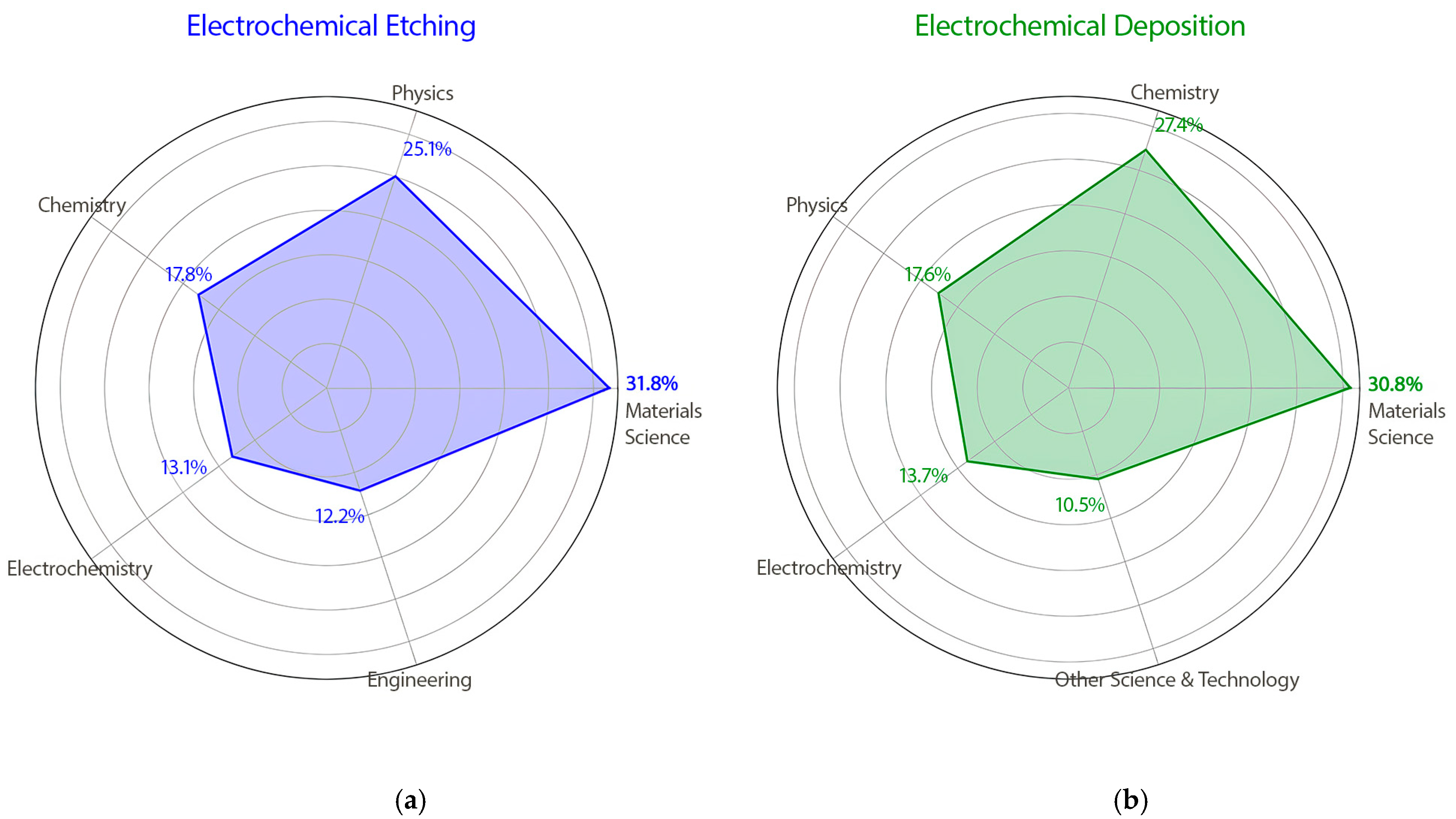
The topic of electrochemical etching spans 55 research areas within SCIE. The largest proportions of publications fall under materials’ science (2215, 42.88%), physics (1745, 33.78%), chemistry (1243, 24.06%), electrochemistry (915, 17.71%), and engineering (847, 16.40%) (Table 2).
The most prolific journals publishing on electrochemical etching include Journal of the Electrochemical Society (264, 5.11%), Electrochimica Acta (179, 3.47%), Applied Surface Science (104, 2.01%), International Journal of Advanced Manufacturing Technology (96, 1.86%), Applied Physics Letters (90, 1.74%), and Nuclear Tracks and Radiation Measurements (74, 1.43%) (Table 3).
The leading publishers in this area are Elsevier (1747, 33.82%), Springer Nature (553, 10.71%), Electrochemical Society Inc. (324, 6.27%), American Chemical Society (278, 5.39%), American Institute of Physics (241, 4.67%), Wiley (234, 4.53%), and IOP Publishing Ltd. (228, 4.41%) (Table 4).
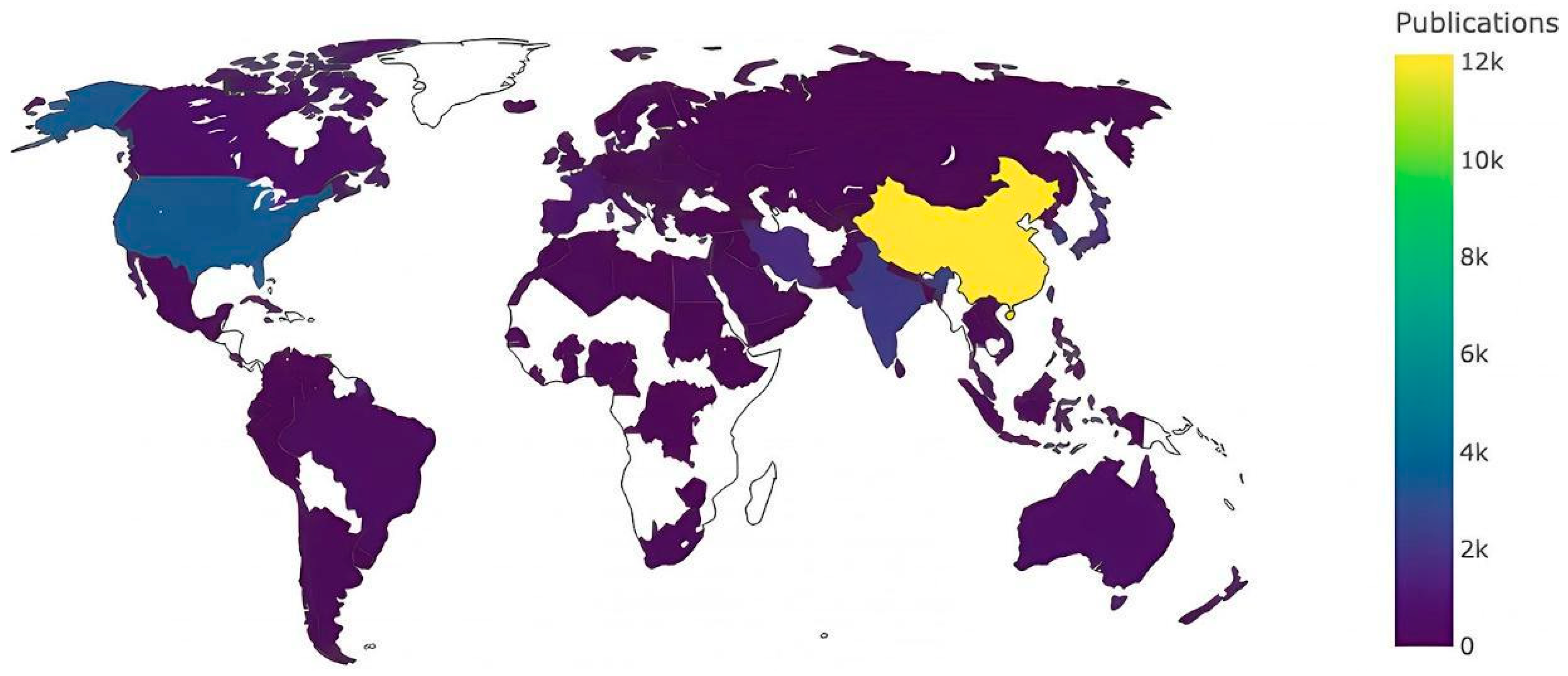
Researchers from China (1208, 23.38%), the USA (585, 11.32%), Germany (403, 7.80%), India (338, 6.54%), Russia (338, 6.54%), and Japan (337, 6.52%) were the most active contributors to this topic (Figure 3). These nations have established themselves as leaders in electrochemical etching research, fostering significant advancements in the field.
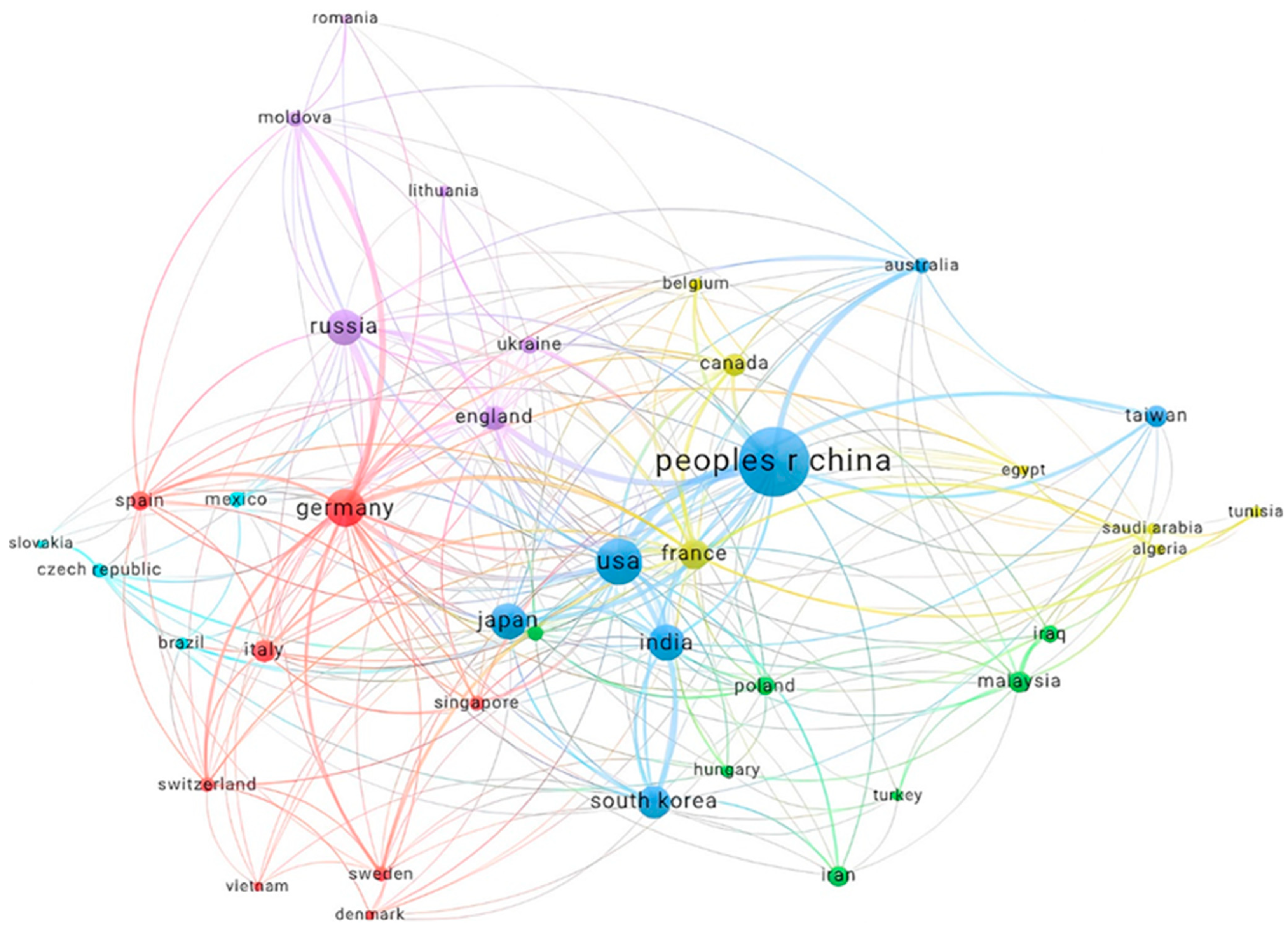
International collaboration plays a critical role in scientific progress, as evidenced by the network of academic partnerships depicted in Figure 4. This figure illustrates the collaborative relationships between the most productive countries, each contributing at least 24 documents. Nodes represent different countries, and the connecting lines indicate cooperation intensity, with line thickness proportional to collaboration strength.
The diagram shows that China is the most central and interconnected node, indicating its significant role in global research collaboration. The United States also emerges as a major hub, reflecting its active participation in international research projects. Germany, Japan, and South Korea are other prominent countries with substantial collaborative links, showcasing their contributions to scientific advancements through partnerships.
European countries such as the UK, France, and Italy demonstrate strong intra-continental collaborations, underscoring the regional emphasis on joint research initiatives. Interestingly, emerging economies like India, Malaysia, and Brazil also feature in the network, indicating their growing involvement in global research efforts. The presence of smaller countries such as Taiwan and Singapore further emphasises the inclusivity and widespread nature of international scientific collaboration.
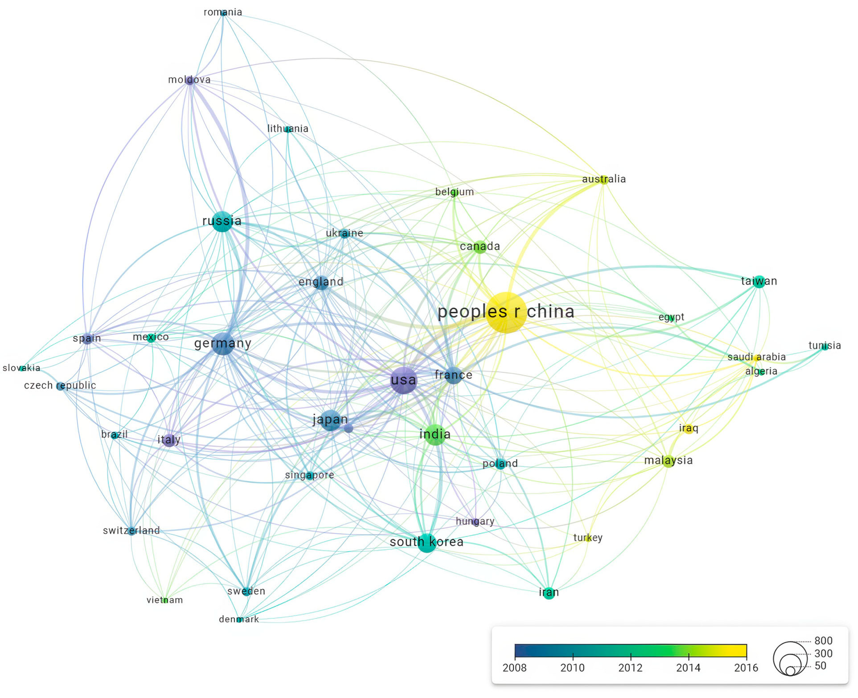
Figure 5 demonstrates the evolution of international collaboration in electrochemical etching research over the years, highlighting the average publication year for each country involved. The colour gradient, ranging from blue to yellow, indicates the average publication year, with blue representing earlier years and yellow representing more recent years.
China stands out as the most prolific contributor, with the highest number of publications (1199 documents), and the average publication year of 2016 indicates a relatively recent surge in research output. The USA also shows a significant number of publications, maintaining a robust presence in the field over time, with an average publication year around 2013. This suggests sustained research activity and collaboration.
Countries like Germany, Japan, and South Korea also feature prominently, with substantial publication records and collaboration networks. Germany’s average publication year is earlier than China’s, reflecting its longer-term engagement in the field. In contrast, Taiwan, Malaysia, and other countries in the Asia-Pacific region show more recent average publication years, highlighting their emerging roles in electrochemical deposition research.
Russia’s position in the network, with its collaborations depicted in purple, indicates earlier average publication years, reflecting a historical focus on this area. However, the recent output from other countries has surpassed it in terms of volume and recency.
The analysis underscores the dynamic nature of international collaboration in electrochemical etching research. While established leaders like China and the USA continue to drive the field, new contributors from the Asia-Pacific region are rapidly increasing their impact, fostering a more diverse and interconnected global research community. This trend highlights the importance of collaborative efforts in advancing the field and suggests a promising future for continued innovation and discovery.
The keywords in scientific papers offer valuable insights into the study’s themes and focal areas. In this analysis, VOSviewer 1.6.20 software was utilised to examine the frequency and co-occurrence of keywords in publications related to electrochemical etching, using SCIE data. A total of 12,621 keywords were identified, of which only 565 appeared 10 or more times. Figure 6 presents the co-occurrence network map of the most frequent keywords, highlighting connections between terms. Each node represents a keyword, and the connecting lines indicate co-occurrence, with node size proportional to keyword linkage and line thickness reflecting co-occurrence frequency.
For this map, keywords with a minimum of 50 occurrences were selected, resulting in 91 keywords. “Electrochemical etching” emerged as the central keyword, exhibiting 564 co-occurrences. Notably, strong associations were observed with “porous silicon” (677 co-occurrences), “fabrication” (494 co-occurrences), and “photoluminescence” (343 co-occurrences).
The co-occurrence analysis revealed three clusters of closely related keywords, each marked with different colours (Figure 5). Cluster 1, represented in red, comprises 32 keywords, focusing on electrochemical dissolution and behaviour. The theme of this cluster centres around the processes and mechanisms of electrochemical dissolution and the resulting behaviours of materials. The publications in this cluster mainly reflect research on interactions at the surface level during electrochemical etching, including the dissolution of different metals and alloys and the effects on microstructure and corrosion resistance.
Cluster 2, shown in green, comprises 31 keywords primarily related to silicon and other semiconductors. This cluster emphasises the use of silicon and other semiconductor materials in various applications. The strong association with photoluminescence and optical properties indicates that the publications mainly reflect a focus on the photonic applications of silicon and other semiconductors. The research concerned the structural and functional modifications of these materials, highlighting the use of nanowires, thin films, and semiconductors for enhanced performance in sensors and solar cells.
Cluster 3, depicted in blue, contains 28 keywords, with an emphasis on nanoparticles and oxidation processes. This cluster concentrates on the oxidation and reduction processes involving nanoparticles. The publications in this cluster show attention to surface interactions and dissolution behaviours of metals and nanoparticles during electrochemical processes. The research emphasises the kinetics of these reactions and their implications for material performance, particularly in terms of passivation and oxidation resistance.
In summary, the keyword co-occurrence network analysis provides a comprehensive overview of the major thematic areas within electrochemical etching research. The identified clusters highlight the focus on electrochemical dissolution processes and material behaviours, the applications and modifications of silicon-based materials, and the oxidation and reduction processes involving nanoparticles. These clusters represent distinct but interconnected areas of research, offering a detailed understanding of the various aspects of electrochemical etching and the materials involved.
The analysis of keywords in the publications also shed light on the most frequently studied materials, including porous silicon (677 occurrences), silicon (303), copper (160), titanium (117), aluminium (96), iron (96), nickel (86), gold (68), stainless steel (58), platinum (53), graphene (48), and silver (41). These materials play pivotal roles in electrochemical etching research and are central to ongoing scientific exploration.
The analysis of keyword co-occurrence data over time for electrochemical etching offers insights into the shifting research trends and focal points within this field (Figure 7). The network map, coloured based on the average publication year, illustrates how different research themes have emerged and evolved from 2010 to 2016. This can be attributed to the year of the appearance of these specific graphs and themes. After 2016, no new dominant themes emerged that had a minimum of 50 occurrences. This may indicate a diversification of research topics, leading to a broader field with a more extensive network that does not exhibit the same dense connections as before.
In the early years, from 2010 to 2012, research primarily focused on fundamental aspects of electrochemical etching. Key topics included “dissolution,” “oxidation,” and “surface” as researchers sought to understand the basic mechanisms and behaviours involved in electrochemical processes. The emphasis was on developing a foundational understanding that could be built upon in subsequent years.
From 2013 to 2014, the focus of research expanded to include more applied aspects, such as “nanoparticles”, “thin films”, and “fabrication”. This period saw significant advancements in the practical applications of electrochemical etching, with an increased emphasis on creating nanostructures and improving fabrication techniques. Researchers explored new materials and methods to enhance the efficiency and effectiveness of electrochemical etching.
In the later years, from 2015 to 2016, the research landscape diversified further, incorporating advanced applications and emerging technologies. Keywords like “photoluminescence”, “optical properties”, and “porous silicon” became more prominent, indicating a growing interest in using electrochemical etching for photonic and optoelectronic applications. The development of “porous silicon” and its integration into various technological applications became a major research focus.
The interconnectedness of different keywords, represented by the strength of the links between them, highlights the collaborative nature of research in this field. Strong connections between keywords such as “electrochemical etching”, “fabrication”, and “porous silicon” demonstrate the multidisciplinary approach adopted by researchers to address complex challenges and innovate within the field.
In summary, the temporal and thematic analysis of electrochemical etching research reveals a dynamic and evolving field. Early research focused on fundamental mechanisms, followed by a shift towards practical applications and advanced technologies. This progression reflects the ongoing efforts of researchers to push the boundaries of what is possible with electrochemical etching and its applications in various industries.

3.2. Electrochemical Deposition

A comprehensive search in the Science Citation Index Expanded (SCIE) database identified a total of 30,759 papers dedicated to electrochemical deposition. The majority of these publications are research articles (29,801, 96.89%), followed by proceeding papers (1451, 4.72%) and review articles (781, 2.54%) (Table 5). The publication trend, as depicted in Figure 8, indicates that interest in electrochemical deposition began to surge in the early 2000s and has maintained a robust growth trajectory to the present day.
Electrochemical deposition research spans 63 distinct areas within the SCIE, with the most substantial contributions coming from materials science (15,354, 49.92%), chemistry (13,623, 44.29%), physics (8763, 28.49%), electrochemistry (6813, 22.15%), and other topics in science and technology (5234, 17.02%) (Table 6).
The most prolific journals publishing on electrochemical deposition include Electrochimica Acta (1558, 5.07%), Journal of the Electrochemical Society (941, 3.06%), Applied Surface Science (752, 2.45%), Journal of Alloys and Compounds (743, 2.42%), Surface Coatings Technology (579, 1.88%), and Journal of Electroanalytical Chemistry (554, 1.80%) (Table 7). These journals are at the forefront of disseminating significant research findings in this field.
Leading publishers in the domain of electrochemical deposition are Elsevier (12,396, 40.30%), the American Chemical Society (2805, 9.12%), Springer Nature (2696, 8.77%), the Royal Society of Chemistry (2332, 7.58%), Wiley (2029, 6.60%), Electrochemical Society Inc. (1142, 3.71%), and MDPI (897, 2.92%). These publishers are instrumental in curating and advancing the scientific discourse on electrochemical deposition (Table 8).
Researchers from China (12,168, 39.56%), the USA (3500, 11.38%), India (2118, 6.89%), South Korea (2083, 6.77%), Iran (1701, 5.53%), Japan (1432, 4.66%), and Germany (1406, 4.57%) have been the most active contributors to this research area (Figure 9). These countries have established themselves as leaders in electrochemical deposition research, demonstrating a strong commitment to advancing the field.
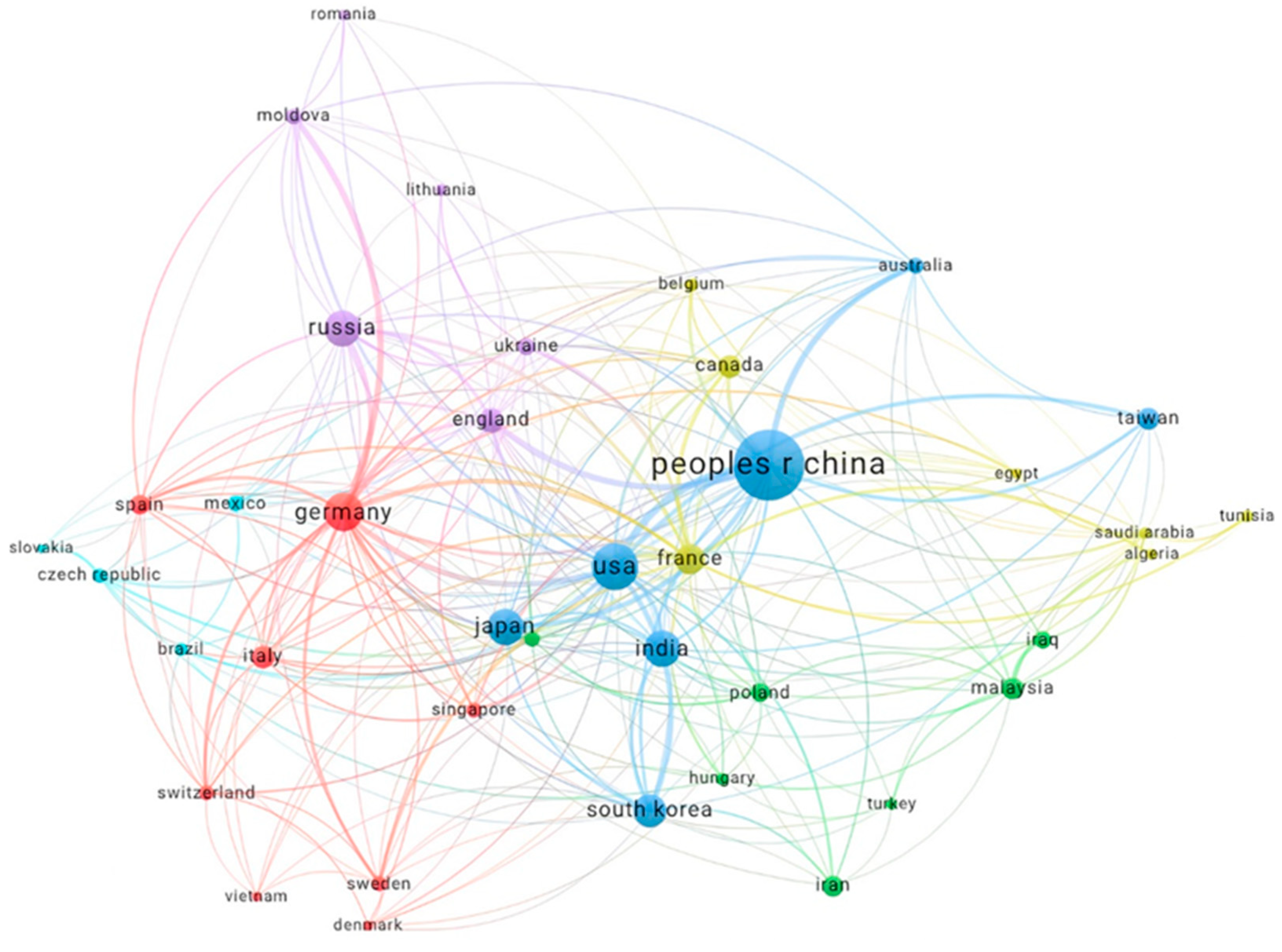
Figure 10 illustrates the international collaboration network among the most prolific countries, each contributing at least 24 documents. China emerges as the most prominent node, reflecting its substantial contribution and central role in global research collaboration. The USA, while also significant, shows fewer connections compared to China, suggesting a more selective collaboration approach.
European countries, particularly Germany, France, and Italy, display dense intra-continental collaboration networks, emphasising the strong regional research partnerships within Europe. Countries like India, South Korea, and Iran are also well-integrated into the global network, showcasing their active participation in international research projects.
The presence of emerging research nations, such as Malaysia, Saudi Arabia, and Egypt, indicates their growing involvement in electrochemical deposition research, contributing to a more diverse and inclusive global research community.
Figure 11 presents an analysis of the international collaboration network in electrochemical deposition research over the years, highlighting the evolution of these collaborations. The nodes are coloured based on the average publication year, with blue indicating earlier years and yellow representing more recent years. This temporal gradient allows us to observe the shifting dynamics of research activity and collaboration intensity.
China stands out as the most prominent node, indicating its significant and recent surge in research output. The concentration of publications around the average year 2016 underscores China’s rapid ascension and dominant role in the field. The USA, while also maintaining a substantial presence, displays a broader range of collaboration over a longer period, with its average publication year around 2013. This suggests a more sustained and consistent research effort.
European countries such as Germany, France, and Italy exhibit dense intra-continental collaboration networks with average publication years indicating a long-term engagement in the field. Germany, with its earlier average publication year, reflects its established history and foundational role, whereas countries like Spain and the UK show a more recent focus, indicating ongoing and evolving research activities.
Emerging research nations, including Malaysia, Saudi Arabia, and Egypt, display more recent average publication years, highlighting their growing involvement and increasing contributions to global research efforts. This trend signifies a broadening of the research community, with new players adding to the diversity and depth of electrochemical deposition research.
In terms of keyword analysis, the VOSviewer software was utilised to evaluate the frequency and co-occurrence of keywords within the publications. This analysis revealed a total of 50,508 keywords, with 3338 occurring 10 times or more. Figure 12 presents a co-occurrence network map of the most frequently occurring keywords, constructed from keywords with at least 50 occurrences, resulting in a network of 850 keywords.
The term “electrodeposition” is notably central within this research field, exhibiting 12,544 co-occurrences with other keywords, indicating its pivotal role in electrochemical deposition studies. Prominent associations are observed with “nanoparticles” (4995 co-occurrences), “fabrication” (3682 co-occurrences), and “films” (2976 co-occurrences), reflecting key themes in the research.
Keywords with strong interconnections were categorised into six distinct clusters, each depicted in different colours (Figure 12). Cluster 1 (red) comprises 226 keywords centred on carbon-based materials and their applications, including carbon nanotubes and graphene. This highlights significant research interest in these materials for their unique properties. Cluster 2 (green) includes 188 keywords related primarily to the surface properties and microstructure of materials, indicating a strong emphasis on understanding and manipulating material surfaces and structures at the microscopic level. Cluster 3 (blue) contains 162 keywords associated with the performance and efficiency of various materials and processes, reflecting the importance of optimising performance metrics in electrochemical deposition. Cluster 4 (yellow) comprises 159 keywords connected to thin films and their optical properties, suggesting a research focus on the fabrication and application of thin film materials in various technologies. Cluster 5 (purple) consists of 86 keywords related to the magnetic properties and related applications of materials, indicating an interest in magnetic materials and their potential uses. Cluster 6 (light blue) includes 29 keywords associated with specific electrochemical processes and techniques, reflecting detailed studies on particular methods within the broader field.
The analysis of keywords also highlighted the materials most frequently studied within electrochemical deposition research. These include copper (1247 occurrences), graphene (1435), nickel (1507), carbon (886), gold (767), graphene oxide (616), silver (523), cobalt (523), silicon (346), and titanium (326). These materials are integral to the research and applications in electrochemical deposition, underscoring their significance in ongoing scientific endeavours.
The analysis of keyword co-occurrence data over time using VOSviewer software reveals the evolution of research trends in electrochemical deposition (Figure 13). The network map, coloured based on the average publication year, provides insights into the shifts in research focus from earlier to more recent studies.
In the early stages of electrochemical deposition research, around the years 2012 to 2014, the focus was predominantly on fundamental aspects and core techniques. Keywords such as “electrodeposition,” “copper,” “nickel,” and “nanoparticles” were central, indicating a primary interest in the basic mechanisms and materials used in electrochemical deposition processes. Studies during this period emphasised understanding the fundamental properties and behaviours of these materials, as well as optimising the deposition techniques for better control and efficiency.
Between 2014 and 2016, there was a noticeable shift towards exploring the applications and performance of deposited materials. Keywords like “performance,” “thin films,” “microstructure,” and “coatings” began to emerge more prominently. This shift reflects a growing interest in applying electrochemical deposition techniques to create advanced materials with specific properties for various applications, such as corrosion resistance, mechanical strength, and electrical conductivity. Research during this period also started to focus on composite materials and the enhancement of material properties through innovative deposition methods.
From 2016 onwards, especially noticeable from 2017 to 2019, the research focus has expanded to include more diverse and application-oriented studies. Keywords such as “nanostructures,” “graphene,” “carbon nanotubes,” “biosensor,” “electrocatalysis,” and “supercapacitor” have become more prevalent. This indicates a strong interest in the functional applications of electrochemically deposited materials in fields such as energy storage, catalysis, and biosensing. The emergence of terms like “facile synthesis,” “efficient,” and “hydrogen evolution reaction” highlights a trend towards developing more efficient and sustainable deposition processes, as well as exploring the potential of these materials in renewable energy technologies.
In summary, the temporal analysis illustrates the dynamic nature of research in electrochemical deposition, with evolving priorities reflecting technological advancements and emerging global challenges. Researchers have progressively moved from foundational studies to application-driven investigations, paving the way for innovative solutions in various high-impact areas.

4. Discussion

4.1. One Technology, Two Modes: Anodic vs. Cathodic Operation

Although this article primarily focuses on bibliometric trends, it is important to briefly outline the technological context in which electrochemical etching and electrochemical deposition are applied. Understanding both methods’ fundamental principles, typical conditions, and materials helps to interpret long-term publication patterns, keyword dynamics, and research trajectories.
It is also important to emphasise that electrochemical etching and electrochemical deposition are two modes of a single technological approach: electrochemical processing. The difference between them lies in electrode polarity and process objective—removing material versus accumulating material.
As noted at the beginning of the article, during electrochemical etching, the substrate is connected as the anode, where oxidation and controlled material dissolution occur. During electrochemical deposition, the substrate acts as the cathode, where reduction leads to the accumulation of material on its surface.
Despite the differences in outcomes, both processes rely on a standard set of key parameters (Table 9).
These parameters are not only fundamental but also strongly interdependent, with each one influencing the outcome of the process in combination with the others. For example, during electrochemical etching, increasing the applied voltage—especially when working with silicon in hydrofluoric acid (HF) electrolytes—accelerates the reaction kinetics, resulting in faster pore formation [80,81,82]. This typically leads to mesoporous structures at moderate voltages, whereas higher voltages can induce a transition to macroporous morphology due to enhanced dissolution rates and local heating effects [83,84].
In electrochemical deposition, the choice of power supply mode plays a crucial role in determining the structural quality of the deposited layer [85,86]. Pulsed current modes, in particular, have proven effective in controlling grain size and suppressing dendritic growth [87,88]. This is especially important when working with metals such as copper or nickel, where uniform layer formation and mechanical stability are essential for applications in microelectronics and energy devices [89,90].
Electrolyte composition and concentration further influence the process outcomes in both methods. In the case of etching, a higher concentration increases the dissolution rate, which may be desirable for fast processing but can also lead to the collapse of delicate porous structures if not carefully controlled [91]. Conversely, in deposition processes, the concentration of metal ions in the electrolyte determines the availability of reactive species at the cathode surface, directly affecting the resulting film’s deposition rate, surface roughness, and thickness uniformity [92].
While external process parameters such as voltage, electrolyte, and current mode play an essential role in shaping the outcomes of electrochemical treatment, the intrinsic properties of the material being processed are often equally decisive. Material-specific factors can significantly alter reaction dynamics, structural outcomes, and functional performance in both etching and deposition.
Silicon (Si) remains the most thoroughly studied and widely used substrate for electrochemical etching. Its predictable behaviour under anodic conditions, compatibility with HF-based electrolytes, and well-understood pore formation mechanisms make it a model system [93]. The ability to form stable and uniform mesoporous and macroporous structures has enabled its use in a wide range of applications, from photonic devices to biosensors and drug delivery systems [94,95].
Complex III–V semiconductors such as gallium arsenide (GaAs) and indium phosphide (InP) have also demonstrated good responsiveness to electrochemical etching, although their behaviour is more sensitive to processing conditions [96]. These materials can form porous layers with large surface areas, making them suitable for optoelectronic and sensing applications [97]. In contrast, II–VI compounds, such as cadmium telluride (CdTe) and zinc selenide (ZnSe), are generally more resistant to electrochemical dissolution, resulting in lower process control and reproducibility [98].
Several intrinsic properties influence how a material responds to electrochemical treatment. The type of conductivity (n-type vs. p-type) strongly affects charge carrier dynamics during etching [99,100]. Doping concentration is another critical factor. Heavily doped substrates often result in thinner, more branched porous structures, while lightly doped materials tend to form more profound and more uniform pores [101]. The crystallographic orientation of the substrate also plays an important role. For instance, Si(100) and Si(111) surfaces exhibit distinct differences in pore shape and propagation due to the atomic arrangement at the surface [102].
These structural differences affect not only the morphology but also the functional properties of the resulting materials. For example, the photoluminescence of porous indium phosphide is highly sensitive to pore size, surface termination, and internal surface area, which are, in turn, governed by the interplay of voltage, doping, and crystal orientation [103]. In deposition processes, the choice of substrate material similarly influences nucleation behaviour, adhesion strength, and film morphology. Surface roughness, chemical compatibility, and lattice mismatch between the deposited material and the substrate determine the structural integrity of the resulting film [104,105]. Thus, electrochemical etching and deposition are highly sensitive to material-related variables that must be considered alongside external process parameters.
The technical overview above highlights the shared foundations and distinct electrochemical etching and deposition behaviour. Despite their different objectives—removal or accumulation of material—these processes rely on a common electrochemical framework governed by voltage, electrolyte chemistry, current regime, and time. However, their performance strongly depends on the processed material’s properties, including conductivity type, doping level, and crystallographic orientation.
This background helps to contextualise specific bibliometric patterns observed in our analysis. For example, the frequent co-occurrence of terms such as porous silicon, photoluminescence, or HF etching can be linked to silicon anodisation’s technological specificity and scientific significance. Similarly, the prominence of copper, nickel, and pulsed deposition in keyword networks reflects ongoing interest in controllable electroplating techniques for electronics, catalysis, and energy storage.
Moreover, international research trends and collaborative clusters may be influenced by thematic interest, material availability, local expertise in semiconductor processing, or access to specialised electrochemical equipment. Recognising the technical underpinnings of these processes thus provides a more informed lens for interpreting the quantitative and qualitative outputs of bibliometric mapping.
While this section is not intended as an exhaustive review of the physical chemistry of electrochemical methods, it serves as a bridge between bibliometric data and the field’s technological reality. It underscores the importance of grounding data-driven analysis in domain-specific knowledge to ensure meaningful interpretation and understanding.

4.2. Comparative Analysis of Research Trends in Electrochemical Etching and Electrochemical Deposition

The comparative analysis of publication trends in electrochemical etching and deposition reveals distinct differences in their respective research outputs over the years. The dataset provides a clear picture of the historical growth and the relative popularity of these two methods in the scientific community (Figure 14).
Electrochemical etching, with a mean publication count of approximately 143.71 and a median of 135, shows a relatively steady output over the years. The highest number of publications in a single year is 282 in 2020, while the lowest is 9 in 1988. The standard deviation is 63.85, indicating moderate variability in the annual publication counts. The coefficient of variation is 0.44, reflecting a consistent but modest fluctuation in research interest.
In contrast, electrochemical deposition exhibits a much higher mean publication count of approximately 623.75 and a median of 642. The highest number of publications in a single year is 2207 in 2022, highlighting a significant peak in research activity. The lowest count is 1, recorded in both 1989 and 1984. The standard deviation is substantially higher at 669.72, indicating a wide range of publication counts across the years. The coefficient of variation is 1.07, showing considerable relative variability, which can be attributed to the dynamic growth in this field.
The publication trends over the years illustrate that electrochemical deposition has consistently garnered more research attention compared to electrochemical etching. The cumulative publication count for deposition has shown a steep increase, particularly from the early 2000s onwards, reflecting its growing importance and widespread application in various industries. Figure 15 provides a visual comparison of the research areas associated with these fields, highlighting both shared and unique domains.
The SCIE indicates that electrochemical etching is primarily explored within the realms of materials science, physics, and chemistry, with a strong focus on innovations in nanostructuring and surface modifications. In contrast, electrochemical deposition covers a wider scope, emphasising electrochemistry and engineering, indicative of its extensive applications in electronics, corrosion protection, and catalysis. While materials science remains a key focus for both processes, electrochemical deposition research includes a broader array of topics, such as thin-film technology and energy storage solutions, showcasing its diverse applications.
An analysis of international contributions reveals that both electrochemical etching and deposition are primarily driven by researchers from leading nations like China, the USA, and Germany. However, the level of contribution and collaboration differs between the fields. China leads in publications in both areas, with a particularly strong influence in electrochemical deposition. Meanwhile, the USA and Germany maintain significant positions, each emphasising different aspects of these processes based on their research priorities.
The comparative analysis of publication trends in electrochemical etching and electrochemical deposition reveals distinct yet interconnected research landscapes, based on our bibliometric analysis (Figure 16).
In the early stages from 1988 to 1990, Germany, the USA, and Japan were prominent in electrochemical etching research, focusing on foundational studies and understanding underlying mechanisms. Similarly, early research in electrochemical deposition during this period centred on fundamental studies and developing core techniques, with significant contributions from the USA and Japan. As our bibliometric analysis shows, the research activities during this period were foundational, setting the stage for future advancements.
From 1990 to 2000, China emerged as a significant player in electrochemical etching research, focusing on application-oriented studies and new materials. During this period, our analysis of publication trends indicates that research in electrochemical deposition saw increased contributions from European countries like Germany and France, with a focus on practical applications, exploring new materials, and improving deposition techniques.
From 2000 to 2010, the research landscape for electrochemical etching diversified, with substantial contributions from India, South Korea, and Taiwan. The bibliometric analysis highlights a shift towards specialised applications, nanostructuring, surface modification, and novel etching techniques. For electrochemical deposition, this period was characterised by a broader range of applications in energy storage, catalysis, and biosensing, with China becoming a central figure in the field. The analysis of keyword co-occurrence during this period shows a clear focus on developing efficient processes and exploring new materials.
Between 2010 and 2020, electrochemical etching research expanded to applied aspects, focusing on nanoparticles, thin films, and fabrication, with leading contributions from China, Germany, and the USA. Our analysis of publication data reveals that electrochemical deposition research during this period included performance and material properties, exploring thin films, microstructure, and coatings. Keywords like “graphene,” “carbon nanotubes,” “biosensor,” “electrocatalysis,” and “supercapacitor” became prevalent, reflecting the trend towards renewable energy technologies and efficient deposition processes.
From 2021 to the present, the research focus in electrochemical etching included diverse applications and new materials in photonics and semiconductor technologies, with China, the USA, and Germany leading the field. As our bibliometric analysis demonstrates, electrochemical deposition research emphasised efficient and sustainable processes, advanced materials, energy storage technologies, and renewable energy applications.
This categorisation, while somewhat arbitrary due to the continuous nature of research progress, provides a broad overview of the shifts in research focus and contributions over time. The analysis underscores the adaptive and innovative nature of scientific inquiry, driven by both foundational studies and application-oriented research. The comparative study highlights the importance of international collaboration and the diverse contributions of different countries, emphasising the global effort to advance electrochemical techniques.

4.3. Future Research Directions

The comparative bibliometric analysis of electrochemical etching and electrochemical deposition reveals that these methods, while historically significant, are currently experiencing a decline in popularity compared to more technologically advanced alternatives, such as atomic layer deposition (ALD) [106], chemical vapour deposition (CVD) [107], and molecular beam epitaxy (MBE) [108]. This trend is reflected in the relatively modest publication landscape (5166 publications for electrochemical etching and 30,759 publications for electrochemical deposition). However, we are convinced that electrochemical methods possess substantial potential due to their undeniable advantages, which position them uniquely in nanostructure synthesis.
Firstly, electrochemical methods have a significant advantage in terms of simplicity of implementation [109,110]. Due to their straightforward nature, these techniques are often referred to as “kitchen” or “bench-top” methods [111,112,113]. Unlike many nanofabrication techniques, electrochemical processes do not require complex procedures or high levels of expertise, making them accessible to a broader range of researchers and industries.
Secondly, electrochemical methods are time-efficient. The processes typically occupy much less time than other high-precision techniques, enabling rapid prototyping and experimentation [114,115]. This time efficiency is particularly beneficial in research settings where quick iterations and adjustments are necessary.
Additionally, electrochemical methods do not require high-vacuum conditions, extreme temperatures, or other unique environments. This lack of stringent requirements makes these processes more accessible to set up and maintain, significantly reducing operational complexity and costs [116,117]. The absence of the need for high-tech equipment further enhances their practicality and economic viability.
Another critical advantage is electrochemical methods’ low cost and economic efficiency [118,119]. Given their simplicity and minimal equipment requirements, the overall expense associated with these processes is relatively low [120,121]. This cost-effectiveness is crucial, especially for industrial applications where large-scale production and budget constraints are important considerations [122].
Electrochemical methods also offer remarkable versatility in forming a wide variety of nanostructures [123,124]. Whether etching intricate patterns [125] or depositing uniform thin films [126], these methods can be tailored to produce diverse nanostructured materials with specific properties. This adaptability is a significant asset in research and industrial applications, where different nanostructures are required for different functionalities.
Furthermore, electrochemical methods’ scalability and adaptability make them suitable for the industrial-scale synthesis of nanostructures [127]. These processes can be easily scaled up from laboratory settings to full-scale production without substantial changes to the methodology [128]. This scalability ensures that the benefits of nanostructured materials can be leveraged in commercial applications effectively and economically.
Additionally, in recent years, combined methods of electrochemical etching and electrochemical deposition have gained traction [129]. Porous layers formed by electrochemical etching can serve as reliable buffer “soft” substrates for subsequent electrochemical deposition [130,131]. This approach mitigates the elastic stresses that typically arise at the interface between two materials, facilitating the formation of high-quality heterostructures [132]. Such combined techniques leverage the strengths of both processes, offering enhanced control over material properties and structural integrity, which is crucial for advanced applications in electronics and photonics [133]. The integration of these methods presents a promising avenue for further research, aiming to optimise and expand their application scope in synthesising nanostructured materials.
Given these advantages, we believe that electrochemical etching and deposition methods are promising for future research and industrial applications. By focusing on optimising these methods and exploring new applications, researchers can continue to unlock their potential. Emerging trends, such as integrating electrochemical techniques with machine learning algorithms for process optimisation and aligning with green chemistry principles to minimise environmental impact, may rejuvenate interest in these methods and expand their applicability across disciplines. Future research should enhance the efficiency, precision, and range of materials and structures produced using electrochemical methods.
In conclusion, despite declining popularity, the inherent advantages of electrochemical methods—such as simplicity, time efficiency, minimal requirements, low cost, versatility, and scalability—underscore their enduring value and potential for future advancements. By capitalising on these strengths, the scientific community can ensure that electrochemical methods remain a vital tool in the synthesis of nanostructures, driving innovation and technological progress.

5. Conclusions

This bibliometric study offers a retrospective and comparative overview of the development of electrochemical etching and electrochemical deposition methods over the period from 1970 to 2023, providing a structured mapping of their research landscapes, key contributors, and thematic evolution.
Our analysis reveals that electrochemical deposition has experienced significantly higher publication activity compared to electrochemical etching, with a notable surge since the early 2000s. Nevertheless, both fields demonstrate sustained scientific interest, reflecting their essential roles in nanomaterial synthesis and functional applications.
The keyword co-occurrence analysis identified how each field evolved: electrochemical etching research moved from fundamental investigations of porous silicon and photoluminescence to photonic and sensing applications, while electrochemical deposition expanded towards energy storage, catalysis, and biosensor technologies. These trends illustrate the gradual specialisation of research topics and the diversification of practical applications.
By analysing the evolution of collaboration networks, we demonstrated the growing importance of international partnerships, with China, the USA, Germany, and emerging research economies playing central roles. The comparative analysis also highlighted shifts in regional leadership over time and the dynamic entry of new contributors.
An important outcome of this work is the comparative perspective: despite operating under a shared electrochemical framework, etching and deposition exhibit distinct thematic trajectories and strategic focuses. Electrochemical etching retains a niche in surface modification and photonics, while electrochemical deposition increasingly supports fields such as renewable energy and advanced coatings.
Although newer fabrication technologies are gaining prominence, electrochemical methods maintain substantial advantages—including simplicity, cost-effectiveness, and scalability—that ensure their relevance for future applications. Especially promising are integrated approaches that combine electrochemical etching and deposition to engineer complex nanostructures.
Thus, this study not only charts the historical development of two fundamental electrochemical techniques but also identifies promising directions for further research and technological innovation. By grounding bibliometric findings in a technological and historical context, we offer insights that can guide future efforts in advancing electrochemical processing for nanomaterials and functional devices.

Author Contributions

Conceptualization, S.N., Y.S., and A.I.P.; methodology, S.N.; software, S.N.; validation, Y.S., A.I.P.; formal analysis, Y.S. and S.N.; investigation, S.N., A.I.P. and Y.S.; resources, S.N.; data curation, S.N. and Y.S.; writing—original draft preparation, Y.S. and S.N.; writing—review and editing, Y.S., S.N., and A.I.P.; visualization, Y.S. and S.N.; supervision, A.I.P.; project administration, Y.S.; funding acquisition, Y.S. All authors have read and agreed to the published version of the manuscript..

Funding

This research was funded by the Ministry of Education and Science of Ukraine under the project 0125U000156 “Buffer Layers for Compositionally-Controlled Heterostructures Used in Photodetectors and Lasers”. Also, Y.S. was partly supported by COST Action CA20129 “Multiscale Irradiation and Chemistry Driven Processes and Related Technologies” (MultIChem) and COST Action CA20126 “Network for research, innovation and product development on porous semiconductors and oxides” (NETPORE).

Institutional Review Board Statement

Not applicable.

Informed Consent Statement

Not applicable.

Data Availability Statement

All data that were used for this research may be found at Zenodo: https://doi.org/10.5281/zenodo.13254743.

Acknowledgments

The authors would like to thank all Ukrainian defenders for the possibility to finalise and publish this work.

Conflicts of Interest

The authors declare that they have no competing financial or non-financial interests.

References

  1. Baig, N.; Kammakakam, I.; Falath, W. Nanomaterials: A review of synthesis methods, properties, recent progress, and challenges. Mater. Adv. 2021, 2, 1821–1871. [Google Scholar] [CrossRef]
  2. Naz, M.Y.; Shukrullah, S.; Ghaffar, A.; Ali, K.; Sharma, S.K. Synthesis and Processing of Nanomaterials. In Solar Cells; Springer International Publishing: Cham, Switzerland, 2020; pp. 1–23. [Google Scholar]
  3. Yun, Q.; Ge, Y.; Shi, Z.; Liu, J.; Wang, X.; Zhang, A.; Huang, B.; Yao, Y.; Luo, Q.; Zhai, L.; et al. Recent Progress on Phase Engineering of Nanomaterials. Chem Rev. 2023, 123, 13489–13692. [Google Scholar] [CrossRef] [PubMed]
  4. Cheng, Z.; Li, M.; Dey, R.; Chen, Y. Nanomaterials for cancer therapy: Current progress and perspectives. J. Hematol. Oncol. 2021, 14, 85. [Google Scholar] [CrossRef]
  5. Verma, A.; Yadav, B.C. Comprehensive review on two-dimensional nanomaterials for optical biosensors: Present progress and outlook. Sustain. Mater. Technol. 2024, 40, e00900. [Google Scholar] [CrossRef]
  6. Afroze, S.; Reza, M.S.; Amin, M.R.; Taweekun, J.; Azad, A.K. Progress in nanomaterials fabrication and their prospects in artificial intelligence towards solid oxide fuel cells: A review. Int. J. Hydrogen Energy 2024, 52, 216–247. [Google Scholar] [CrossRef]
  7. Khan, F.A. Synthesis of Nanomaterials: Methods & Technology. In Applications of Nanomaterials in Human Health; Springer: Singapore, 2020; pp. 15–21. [Google Scholar]
  8. Gutiérrez-Cruz, A.; Ruiz-Hernández, A.R.; Vega-Clemente, J.F.; Luna-Gazcón, D.G.; Campos-Delgado, J. A review of top-down and bottom-up synthesis methods for the production of graphene, graphene oxide and reduced graphene oxide. J. Mater. Sci. 2022, 57, 14543–14578. [Google Scholar] [CrossRef]
  9. Wen, B.; Yang, J.; Hu, C.; Cai, J.; Zhou, J. Top-Down Fabrication of Ordered Nanophotonic Structures for Biomedical Applications. Adv. Mater. Interfaces 2024, 11, 856. [Google Scholar] [CrossRef]
  10. Chen, F.; Yan, T.H.; Bashir, S.; Liu, J.L. Synthesis of nanomaterials using top-down methods. In Advanced Nanomaterials and Their Applications in Renewable Energy; Elsevier: Amsterdam, The Netherlands, 2022; pp. 37–60. [Google Scholar]
  11. Abid, N.; Khan, A.M.; Shujait, S.; Chaudhary, K.; Ikram, M.; Imran, M.; Haider, J.; Khan, M.; Khan, Q.; Maqbool, M. Synthesis of nanomaterials using various top-down and bottom-up approaches, influencing factors, advantages, and disadvantages: A review. Adv. Colloid Interface Sci. 2022, 300, 102597. [Google Scholar] [CrossRef]
  12. El-Khawaga, A.M.; Zidan, A.; El-Mageed, A.I.A.A. Preparation methods of different nanomaterials for various potential applications: A Review. J. Mol. Struct. 2023, 1281, 135148. [Google Scholar] [CrossRef]
  13. Jiang, Z.; Li, L.; Huang, H.; He, W.; Ming, W. Progress in Laser Ablation and Biological Synthesis Processes: “Top-Down” and “Bottom-Up” Approaches for the Green Synthesis of Au/Ag Nanoparticles. Int. J. Mol. Sci. 2022, 23, 14658. [Google Scholar] [CrossRef]
  14. Lombardo, D.; Calandra, P.; Pasqua, L.; Magazù, S. Self-Assembly of Organic Nanomaterials and Biomaterials: The Bottom-Up Approach for Functional Nanostructures Formation and Advanced Applications. Materials 2020, 13, 1048. [Google Scholar] [CrossRef] [PubMed]
  15. Pang, C.; Aryal, B.R.; Ranasinghe, D.R.; Westover, T.R.; Ehlert, A.E.F.; Harb, J.N.; Davis, R.C.; Woolley, A.T. Bottom-Up Fabrication of DNA-Templated Electronic Nanomaterials and Their Characterization. Nanomaterials 2021, 11, 1655. [Google Scholar] [CrossRef]
  16. Cook, A.B.; Clemons, T.D. Bottom-Up versus Top-Down Strategies for Morphology Control in Polymer-Based Biomedical Materials. Adv. NanoBiomed Res. 2021, 2, 2100087. [Google Scholar] [CrossRef]
  17. Fu, Y.Q.; Colli, A.; Fasoli, A.; Luo, J.K.; Flewitt, A.J.; Ferrari, A.C.; Milne, W.I. Deep reactive ion etching as a tool for nanostructure fabrication. J. Vac. Sci. Technol. B Microelectron. Nanometer Struct. 2009, 27, 1520. [Google Scholar] [CrossRef]
  18. Kunuku, S.; Sankaran, K.J.; Tsai, C.-Y.; Chang, W.-H.; Tai, N.-H.; Leou, K.-C.; Lin, I.-N. Investigations on Diamond Nanostructuring of Different Morphologies by the Reactive-Ion Etching Process and Their Potential Applications. ACS Appl. Mater. Interfaces 2013, 5, 7439–7449. [Google Scholar] [CrossRef]
  19. Matsui, S.; Kaito, T.; Fujita, J.-i.; Komuro, M.; Kanda, K.; Haruyama, Y. Three-dimensional nanostructure fabrication by focused-ion-beam chemical vapor deposition. J. Vac. Sci. Technol. B Microelectron. Nanometer Struct. 2000, 18, 3181–3184. [Google Scholar] [CrossRef]
  20. Cai, Z.; Liu, B.; Zou, X.; Cheng, H.-M. Chemical Vapor Deposition Growth and Applications of Two-Dimensional Materials and Their Heterostructures. Chem. Rev. 2018, 118, 6091–6133. [Google Scholar] [CrossRef] [PubMed]
  21. Tan, Q.; Lu, F.; Xue, C.; Zhang, W.; Lin, L.; Xiong, J. Nano-fabrication methods and novel applications of black silicon. Sens. Actuators A Phys. 2019, 295, 560–573. [Google Scholar] [CrossRef]
  22. Lv, H.; Pan, Q.; Song, Y.; Liu, X.-X.; Liu, T. A Review on Nano-/Microstructured Materials Constructed by Electrochemical Technologies for Supercapacitors. Nano-Micro Lett. 2020, 12, 118. [Google Scholar] [CrossRef]
  23. Crapnell, R.D.; Banks, C.E. Electroanalytical overview: Utilising micro- and nano-dimensional sized materials in electrochemical-based biosensing platforms. Microchim. Acta 2021, 188, 268. [Google Scholar] [CrossRef]
  24. Li, H.; Li, H.; Lai, Y.; Yang, Z.; Yang, Q.; Liu, Y.; Zheng, Z.; Liu, Y.; Sun, Y.; Zhong, B.; et al. Revisiting the Preparation Progress of Nano-Structured Si Anodes toward Industrial Application from the Perspective of Cost and Scalability. Adv. Energy Mater. 2022, 12, 2102181. [Google Scholar] [CrossRef]
  25. Garlyyev, B.; Watzele, S.; Fichtner, J.; Michalička, J.; Schökel, A.; Senyshyn, A.; Perego, A.; Pan, D.; El-Sayed, H.A.; Macak, J.M.; et al. Electrochemical top-down synthesis of C-supported Pt nanoparticles with controllable shape and size: Mechanistic insights and application. Nano Res. 2021, 14, 2762–2769. [Google Scholar] [CrossRef]
  26. Maleski, K.; Alhabeb, M. Top-Down MXene Synthesis (Selective Etching). In 2D Metal Carbides and Nitrides (MXenes); Anasori, B., Gogotsi, Y., Eds.; Springer: Cham, Switzerland, 2019. [Google Scholar]
  27. Li, C.; Iqbal, M.; Lin, J.; Luo, X.; Jiang, B.; Malgras, V.; Wu, K.C.-W.; Kim, J.; Yamauchi, Y. Electrochemical Deposition: An Advanced Approach for Templated Synthesis of Nanoporous Metal Architectures. Acc. Chem. Res. 2018, 51, 1764–1773. [Google Scholar] [CrossRef] [PubMed]
  28. Huang, B.; Cai, Z.; Peng, T.; Tan, Y.; Zhang, N.; Liu, W.; Zhong, H.; Mai, Y. Bottom-up deposition lithium into 3D lithiophobic-lithiophilic host for long-life lithium metal anodes. J. Mater. Chem. A 2024, 12, 13733–13741. [Google Scholar] [CrossRef]
  29. Suchikova, Y.; Kidalov, V.; Sukach, G. Influence of dislocations on the process of pore formation in n-InP (111) single crystals. Semiconductors. 2011, 45, 121–124. [Google Scholar] [CrossRef]
  30. Xu, J.; Liu, S.; Yang, Y.; Li, J.; Tian, C.; Guo, L.; Zhang, S.; Liu, Y.; Zhong, Z. Preparation of Porous Silicon by Electrochemical Etching Methods and its Morphological and Optical Properties. Int. J. Electrochem. Sci. 2019, 14, 5188–5199. [Google Scholar] [CrossRef]
  31. Surdo, S.; Barillaro, G. Voltage- and Metal-assisted Chemical Etching of Micro and Nano Structures in Silicon: A Comprehensive Review. Small 2024, 20, e2400499. [Google Scholar] [CrossRef]
  32. Ding, Y.; Liu, Z.; Liu, L.; Li, Z. A surface micromachining process for suspended RF-MEMS applications using porous silicon. Microsyst. Technol. 2003, 9, 470–473. [Google Scholar] [CrossRef]
  33. Ervin, M.H.; Piekiel, N.W.; Isaacson, B. Process for integrating porous silicon with other devices. Sens. Actuators A Phys. 2018, 280, 132–138. [Google Scholar] [CrossRef]
  34. Kim, H.; Seo, H.G.; Choi, Y.; Lim, D.-K.; Jung, W. Cathodic electrochemical deposition: A new strategy to enhance the activity and stability of silver cathodes for thin-film solid oxide fuel cells. J. Mater. Chem. A. 2020, 8, 14491–14497. [Google Scholar] [CrossRef]
  35. Cuevas, A.L.; Dominguez, A.; Zamudio-García, J.; Vega, V.; González, A.S.; Marrero-López, D.; Prida, V.M.; Benavente, J. Optical and Electrochemical Properties of a Nanostructured ZnO Thin Layer Deposited on a Nanoporous Alumina Structure via Atomic Layer Deposition. Materials 2024, 17, 1412. [Google Scholar] [CrossRef]
  36. Tonelli, D.; Scavetta, E.; Gualandi, I. Electrochemical Deposition of Nanomaterials for Electrochemical Sensing. Sensors 2019, 19, 1186. [Google Scholar] [CrossRef] [PubMed]
  37. Bocchetta, P.; Frattini, D.; Tagliente, M.; Selleri, F. Electrochemical Deposition of Polypyrrole Nanostructures for Energy Applications: A Review. Curr. Nanosci. 2020, 16, 462–477. [Google Scholar] [CrossRef]
  38. Prida, V.M.; Vega, V.; García, J.; Iglesias, L.; Hernando, B.; Minguez-Bacho, I. Electrochemical methods for template-assisted synthesis of nanostructured materials. In Magnetic Nano- and Microwires; Elsevier: Amsterdam, The Netherlands, 2015; pp. 3–39. [Google Scholar]
  39. Xian, X.; Jiao, L.; Xue, T.; Wu, Z.; Liu, Z. Nanoveneers: An Electrochemical Approach to Synthesizing Conductive Layered Nanostructures. ACS Nano 2011, 5, 4000–4006. [Google Scholar] [CrossRef]
  40. Zhang, Z.; Feng, C.; Liu, C.; Zuo, M.; Qin, L.; Yan, X.; Xing, Y.; Li, H.; Si, R.; Zhou, S.; et al. Electrochemical deposition as a universal route for fabricating single-atom catalysts. Nat. Commun. 2020, 11, 1215. [Google Scholar] [CrossRef]
  41. Bernal Lopez, M.; Ustarroz, J. Electrodeposition of nanostructured catalysts for electrochemical energy conversion: Current trends and innovative strategies. Curr. Opin. Electrochem. 2021, 27, 100688. [Google Scholar] [CrossRef]
  42. Zhong, Y.; Xu, X.; Veder, J.-P.; Shao, Z. Self-Recovery Chemistry and Cobalt-Catalyzed Electrochemical Deposition of Cathode for Boosting Performance of Aqueous Zinc-Ion Batteries. iScience 2020, 23, 100943. [Google Scholar] [CrossRef]
  43. Barim, S.B.; Uzunlar, E.; Bozbag, S.E.; Erkey, C. Review—Supercritical Deposition: A Powerful Technique for Synthesis of Functional Materials for Electrochemical Energy Conversion and Storage. J. Electrochem. Soc. 2020, 167, 054510. [Google Scholar] [CrossRef]
  44. Shi, Y.; Huang, W.M.; Li, J.; Zhou, Y.; Li, Z.-Q.; Yin, Y.-C.; Xia, X.-H. Site-specific electrodeposition enables self-terminating growth of atomically dispersed metal catalysts. Nat. Commun. 2020, 11, 4558. [Google Scholar] [CrossRef]
  45. Lee, S.; Jang, J.; Park, T.; Park, Y.M.; Park, J.S.; Kim, Y.-K.; Lee, H.-K.; Jeon, E.-C.; Lee, D.-K.; Ahn, B.; et al. Electrodeposited Silver Nanowire Transparent Conducting Electrodes for Thin-Film Solar Cells. ACS Appl. Mater. Interfaces 2020, 12, 6169–6175. [Google Scholar] [CrossRef]
  46. Manoharan, S.; Krishnamoorthy, K.; Mariappan, V.K.; Kesavan, D.; Kim, S.-J. Electrochemical deposition of vertically aligned tellurium nanorods on flexible carbon cloth for wearable supercapacitors. Chem. Eng. J. 2021, 421, 129548. [Google Scholar] [CrossRef]
  47. Paradowska, E.; Arkusz, K.; Pijanowska, D.G. Comparison of Gold Nanoparticles Deposition Methods and Their Influence on Electrochemical and Adsorption Properties of Titanium Dioxide Nanotubes. Materials 2020, 13, 4269. [Google Scholar] [CrossRef]
  48. Mavukkandy, M.O.; McBride, S.A.; Warsinger, D.M.; Dizge, N.; Hasan, S.W.; Arafat, H.A. Thin film deposition techniques for polymeric membranes—A review. J. Membr. Sci. 2020, 610, 118258. [Google Scholar] [CrossRef]
  49. Roy, D.; Srivastava, A.K.; Mukhopadhyay, K.; Namburi, E.P. 0D, 1D, 2D & 3D Nano Materials: Synthesis and Applications. In Novel Defence Functional and Engineering Materials (NDFEM) Volume 1; Springer: Singapore, 2024; pp. 73–91. [Google Scholar]
  50. Marinoiu, A.; Raceanu, M.; Andrulevicius, M.; Tamuleviciene, A.; Tamulevicius, T.; Nica, S.; Bala, D.; Varlam, M. Low-cost preparation method of well dispersed gold nanoparticles on reduced graphene oxide and electrocatalytic stability in PEM fuel cell. Arab. J. Chem. 2020, 13, 3585–3600. [Google Scholar] [CrossRef]
  51. Liu, J.; Fang, X.; Zhu, C.; Xing, X.; Cui, G.; Li, Z. Fabrication of superhydrophobic coatings for corrosion protection by electrodeposition: A comprehensive review. Colloids Surf. A Physicochem. Eng. Asp. 2020, 607, 125498. [Google Scholar] [CrossRef]
  52. Walsh, F.C.; Ponce de León, C. Versatile electrochemical coatings and surface layers from aqueous methanesulfonic acid. Surf. Coat. Technol. 2014, 259, 676–697. [Google Scholar] [CrossRef]
  53. Davydov, A.D.; Volgin, V.M. Electrochemical Local Maskless Micro/Nanoscale Deposition, Dissolution, and Oxidation of Metals and Semiconductors: A Review. Russ. J. Electrochem. 2020, 56, 52–81. [Google Scholar] [CrossRef]
  54. Conway, B.E.; Kannangara, D.C.W. Zinc Oxidation and Redeposition Processes in Aqueous Alkali and Carbonate Solutions: II. Distinction Between Dissolution and Oxide Film Formation Processes. J. Electrochem. Soc. 1987, 134, 906–918. [Google Scholar] [CrossRef]
  55. Lai, C.Q.; Zheng, W.; Choi, W.K.; Thompson, C.V. Metal assisted anodic etching of silicon. Nanoscale 2015, 7, 11123–11134. [Google Scholar] [CrossRef]
  56. Cao, A.T.; Luong, Q.N.T.; Dao, C.T. Influence of the anodic etching current density on the morphology of the porous SiC layer. AIP Adv. 2014, 4, 037105. [Google Scholar] [CrossRef]
  57. Blackwood, D.J.; Seah, K.H.W. Electrochemical cathodic deposition of hydroxyapatite: Improvements in adhesion and crystallinity. Mater. Sci. Eng. C 2009, 29, 1233–1238. [Google Scholar] [CrossRef]
  58. Sanders, D.M.; Anders, A. Review of cathodic arc deposition technology at the start of the new millennium. Surf. Coat. Technol. 2000, 133–134, 78–90. [Google Scholar] [CrossRef]
  59. Schultze, J.W.; Bressel, A. Principles of electrochemical micro- and nano-system technologies. Electrochim. Acta 2001, 47, 3–21. [Google Scholar] [CrossRef]
  60. Torres-Costa, V.; Martín-Palma, R.J. Application of nanostructured porous silicon in the field of optics: A review. J. Mater. Sci. 2010, 45, 2823–2838. [Google Scholar] [CrossRef]
  61. Arshavsky-Graham, S.; Massad-Ivanir, N.; Segal, E.; Weiss, S. Porous Silicon-Based Photonic Biosensors: Current Status and Emerging Applications. Anal. Chem. 2018, 91, 441–467. [Google Scholar] [CrossRef] [PubMed]
  62. Dhanekar, S.; Jain, S. Porous silicon biosensor: Current status. Biosens. Bioelectron. 2013, 41, 54–64. [Google Scholar] [CrossRef] [PubMed]
  63. Stalmans, L.; Poortmans, J.; Bender, H.; Caymax, M.; Said, K.; Vazsonyi, E.; Nijs, J.; Mertens, R. Porous silicon in crystalline silicon solar cells: A review and the effect on the internal quantum efficiency. Prog. Photovolt. Res. Appl. 1998, 6, 233–246. [Google Scholar] [CrossRef]
  64. Dubey, R.S.; Gautam, D.K. Porous silicon layers prepared by electrochemical etching for application in silicon thin film solar cells. Superlattices Microstruct. 2011, 50, 269–276. [Google Scholar] [CrossRef]
  65. Yuda, A.P.; Koraag, P.Y.E.; Iskandar, F.; Wasisto, H.S.; Sumboja, A. Advances of the top-down synthesis approach for high-performance silicon anodes in Li-ion batteries. J. Mater. Chem. A 2021, 9, 18906–18926. [Google Scholar] [CrossRef]
  66. Suchikova, Y.; Kovachov, S.; Bohdanov, I.; Kozlovskiy, A.L.; Zdorovets, M.V.; Popov, A.I. Improvement of β-SiC Synthesis Technology on Silicon Substrate. Technologies 2023, 11, 152. [Google Scholar] [CrossRef]
  67. Schmuki, P.; Santinacci, L.; Djenizian, T.; Lockwood, D.J. Pore Formation on n-InP. Phys. Status Solidi A 2000, 182, 51–61. [Google Scholar] [CrossRef]
  68. Langa, S.; Tiginyanu, I.M.; Monaico, E.; Föll, H. Porous II–VI vs. porous III–V semiconductors. Phys. Status Solidi C 2011, 8, 1792–1796. [Google Scholar] [CrossRef]
  69. Suchikova, Y.; Lysak, A.; Kovachov, S.; Konuhova, M.; Zhydachevskyy, Y.; Popov, A.I. Investigation of the Impact of Crystalline Arsenolite Oxide Formations on Porous Gallium Arsenide. Phys. Status Solidi (a) 2024, 221, 2400365. [Google Scholar] [CrossRef]
  70. Monaico, E.V.; Morari, V.; Ursaki, V.V.; Nielsch, K.; Tiginyanu, I.M. Core–Shell GaAs-Fe Nanowire Arrays: Fabrication Using Electrochemical Etching and Deposition and Study of Their Magnetic Properties. Nanomaterials 2022, 12, 1506. [Google Scholar] [CrossRef] [PubMed]
  71. Moise, C.C.; Mihai, G.V.; Anicăi, L.; Monaico, E.V.; Ursaki, V.V.; Enăchescu, M.; Tiginyanu, I.M. Electrochemical Deposition of Ferromagnetic Ni Nanoparticles in InP Nanotemplates Fabricated by Anodic Etching Using Environmentally Friendly Electrolyte. Nanomaterials 2022, 12, 3787. [Google Scholar] [CrossRef]
  72. Ellegaard, O.; Wallin, J.A. The bibliometric analysis of scholarly production: How great is the impact? Scientometrics 2015, 105, 1809–1831. [Google Scholar] [CrossRef]
  73. Passas, I. Bibliometric Analysis: The Main Steps. Encyclopedia 2024, 4, 1014–1025. [Google Scholar] [CrossRef]
  74. Menéndez-Manjón, A.; Moldenhauer, K.; Wagener, P.; Barcikowski, S. Nano-energy research trends: Bibliometrical analysis of nanotechnology research in the energy sector. J. Nanopart. Res. 2011, 13, 3911–3922. [Google Scholar] [CrossRef]
  75. Sales, M.B.; Neto, J.G.L.; De Sousa Braz, A.K.; De Sousa Junior, P.G.; Melo, R.L.F.; Valério, R.B.R.; Serpa, J.d.F.; Da Silva Lima, A.M.; De Lima, R.K.C.; Guimarães, A.P.; et al. Trends and Opportunities in Enzyme Biosensors Coupled to MOFs: An Advanced Bibliometric Analysis. Electrochem 2023, 4, 181–211. [Google Scholar] [CrossRef]
  76. Zhang, F.; Xu, W.; Deng, Z.; Huang, J. A bibliometric and visualization analysis of electrochemical biosensors for early diagnosis of eye diseases. Front. Med. 2025, 11, 1487981. [Google Scholar] [CrossRef]
  77. Suchikova, Y.; Nazarovets, S.; Popov, A.I. Ga2O3 Solar-Blind Photodetectors: From Civilian Applications to Missile Detection and Research Agenda. Opt. Mater. 2024, 157, 116397. [Google Scholar] [CrossRef]
  78. Mongeon, P.; Paul-Hus, A. The journal coverage of Web of Science and Scopus: A comparative analysis. Scientometrics 2016, 106, 213–228. [Google Scholar] [CrossRef]
  79. van Eck, N.J.; Waltman, L. Software survey: VOSviewer, a computer program for bibliometric mapping. Scientometrics 2010, 84, 523–538. [Google Scholar] [CrossRef] [PubMed]
  80. Suchikova, Y.O.; Bogdanov, I.T.; Kovachov, S.S.; Kamensky, D.V.; Myroshnychenko, V.O.; Panova, N.Y. Optimal ranges determination of morphological parameters of nanopatterned semiconductors quality for solar cells. Arch. Mater. Sci. Eng. 2020, 1, 15–24. [Google Scholar] [CrossRef]
  81. Al-Rahime, N.M.; Salman, H.I.; Al-Kadumi, A.K. The effect of different HF concentrations on porous silicon formation. In Proceedings of the International Conference of Computational Methods in Sciences and Engineering (ICCMSE 2021), Karbala, Iraq, 6 April 2021; AIP Publishing: Melville, NY, USA, 2023. [Google Scholar] [CrossRef]
  82. Kleimann, P.; Linnros, J.; Petersson, S. Formation of wide and deep pores in silicon by electrochemical etching. Mater. Sci. Eng. B 2000, 69–70, 29–33. [Google Scholar] [CrossRef]
  83. Vambol, S.; Bogdanov, I.; Vambol, V.; Suchikova, Y.; Lopatina, H.; Tsybuliak, N. Research into effect of electrochemical etching conditions on the morphology of porous gallium arsenide. East.-Eur. J. Enterp. Technol. 2017, 6, 22–31. [Google Scholar] [CrossRef]
  84. Sychikova, Y.A.; Kidalov, V.V.; Sukach, G.A. Dependence of the threshold voltage in indium-phosphide pore formation on the electrolyte composition. J. Surf. Investig. X-Ray Synchrotron Neutron Tech. 2013, 7, 626–630. [Google Scholar] [CrossRef]
  85. Suchikova, Y.; Kovachov, S.; Bohdanov, I. Formation of oxide crystallites on the porous GaAs surface by electrochemical deposition. Nanomater. Nanotechnol. 2022, 12, 184798042211273. [Google Scholar] [CrossRef]
  86. Larson, C.; Farr, J.P.G. Current research and potential applications for pulsed current electrodeposition—A review. Trans. IMF 2012, 90, 20–29. [Google Scholar] [CrossRef]
  87. Reisecker, V.; Flatscher, F.; Porz, L.; Fincher, C.; Todt, J.; Hanghofer, I.; Hennige, V.; Linares-Moreau, M.; Falcaro, P.; Ganschow, S.; et al. Effect of pulse-current-based protocols on the lithium dendrite formation and evolution in all-solid-state batteries. Nat. Commun. 2023, 14, 2432. [Google Scholar] [CrossRef]
  88. Sharma, A.; Bhattacharya, S.; Das, S.; Das, K. A Study on the Effect of Pulse Electrodeposition Parameters on the Morphology of Pure Tin Coatings. Metall. Mater. Trans. A 2014, 45, 4610–4622. [Google Scholar] [CrossRef]
  89. Bhardwaj, M.; Balani, K.; Balasubramaniam, R.; Pandey, S.; Agarwal, A. Effect of current density and grain refining agents on pulsed electrodeposition of nanocrystalline nickel. Surf. Eng. 2011, 27, 642–648. [Google Scholar] [CrossRef]
  90. Kurniawan, M.; Ivanov, S. Electrochemically Structured Copper Current Collectors for Application in Energy Conversion and Storage: A Review. Energies 2023, 16, 4933. [Google Scholar] [CrossRef]
  91. Solanki, C.S.; Bilyalov, R.R.; Poortmans, J.; Celis, J.P.; Nijs, J. Effect of the composition of electrolyte on separation of porous silicon film by electrochemical etching. Phys. Status Solidi A 2003, 197, 507–511. [Google Scholar] [CrossRef]
  92. Suchikova, Y.; Kovachov, S.; Lazarenko, A.; Bohdanov, I. Research of synthesis conditions and structural features of heterostructure AlXGa1–XAs/GaAs of the “desert rose” type. Appl. Surf. Sci. Adv. 2022, 12, 100327. [Google Scholar] [CrossRef]
  93. Kuntyi, O.; Zozulya, G.; Shepida, M. Porous Silicon Formation by Electrochemical Etching. Adv. Mater. Sci. Eng. 2022, 2022, 1482877. [Google Scholar] [CrossRef]
  94. Shinde, P.S.; Suryawanshi, P.S.; Patil, K.K.; Belekar, V.M.; Sankpal, S.A.; Delekar, S.D.; Jadhav, S.A. A Brief Overview of Recent Progress in Porous Silica as Catalyst Supports. J. Compos. Sci. 2021, 5, 75. [Google Scholar] [CrossRef]
  95. Moretta, R.; De Stefano, L.; Terracciano, M.; Rea, I. Porous Silicon Optical Devices: Recent Advances in Biosensing Applications. Sensors 2021, 21, 1336. [Google Scholar] [CrossRef]
  96. Vambol, S.; Bogdanov, I.; Vambol, V.; Suchikova, Y.; Kondratenko, O.; Hurenko, O.; Onishchenko, S. Research into regularities of pore formation on the surface of semiconductors. East.-Eur. J. Enterp. Technol. 2017, 3, 37–44. [Google Scholar] [CrossRef]
  97. van Dorp, D.H.; Arnauts, S.; Laitinen, M.; Sajavaara, T.; Meersschaut, J.; Conard, T.; Kelly, J.J. Nanoscale etching of III–V semiconductors in acidic hydrogen peroxide solution: GaAs and InP, a striking contrast in surface chemistry. Appl. Surf. Sci. 2019, 465, 596–606. [Google Scholar] [CrossRef]
  98. Lemasson, P. Electrochemistry: A versatile technique for investigation of bulk and surface properties of II–VI compounds. J. Cryst. Growth 1985, 72, 405–418. [Google Scholar] [CrossRef]
  99. Izuo, S.; Ohji, H.; French, P.J.; Tsutsumi, K. A novel electrochemical etching technique for n-type silicon. Sens. Actuators A Phys. 2002, 97–98, 720–724. [Google Scholar] [CrossRef]
  100. Ohji, H.; French, P.J.; Tsutsumi, K. Fabrication of mechanical structures in p-type silicon using electrochemical etching. Sens. Actuators A Phys. 2000, 82, 254–258. [Google Scholar] [CrossRef]
  101. Allongue, P.; Blonkowski, S. Influence of the doping concentration on the electrochemical etching of semiconductors. Electrochim. Acta 1993, 38, 889–895. [Google Scholar] [CrossRef]
  102. Allongue, P.; Costa-Kieling, V.; Gerischer, H. Etching of Silicon in NaOH Solutions: II. Electrochemical Studies of n-Si(111) and (100) and Mechanism of the Dissolution. J. Electrochem. Soc. 1993, 140, 1018–1026. [Google Scholar] [CrossRef]
  103. Suchikova, Y.; Kidalov, V.; Sukach, G. Blue Shift of Photoluminescence Spectrum of Porous InP. ECS Trans. 2019, 25, 59–64. [Google Scholar] [CrossRef]
  104. Suchikova, Y.; Kovachov, S.; Bohdanov, I.; Konuhova, M.; Zhydachevskyy, Y.; Kumarbekov, K.; Pankratov, V.; Popov, A.I. Wet Chemical Synthesis of AlxGa1−xAs Nanostructures: Investigation of Properties and Growth Mechanisms. Crystals 2024, 14, 633. [Google Scholar] [CrossRef]
  105. Suchikova, Y.; Kovachov, S.; Bohdanov, I.; Karipbayev, Z.T.; Zhydachevskyy, Y.; Lysak, A.; Pankratov, V.; Popov, A.I. Advanced Synthesis and Characterization of CdO/CdS/ZnO Heterostructures for Solar Energy Applications. Materials 2024, 17, 1566. [Google Scholar] [CrossRef]
  106. Cremers, V.; Puurunen, R.L.; Dendooven, J. Conformality in atomic layer deposition: Current status overview of analysis and modelling. Appl. Phys. Rev. 2019, 6, 021302. [Google Scholar] [CrossRef]
  107. Pant, M.; Singh, R.; Negi, P.; Tiwari, K.; Singh, Y. A comprehensive review on carbon nano-tube synthesis using chemical vapor deposition. Mater. Today Proc. 2021, 46, 11250–11253. [Google Scholar] [CrossRef]
  108. Nunn, W.; Truttmann, T.K.; Jalan, B. A review of molecular-beam epitaxy of wide bandgap complex oxide semiconductors. J. Mater. Res. 2021, 36, 4846–4864. [Google Scholar] [CrossRef]
  109. Ma, N.; Cheng, D.; Zhang, J.; Zhao, S.; Lu, Y. A simple, inexpensive and environmental-friendly electrochemical etching method to fabricate superhydrophobic GH4169 surfaces. Surf. Coat. Technol. 2020, 399, 126180. [Google Scholar] [CrossRef]
  110. Du, D.; Liu, J.; Zhang, X.; Cui, X.; Lin, Y. One-step electrochemical deposition of a graphene-ZrO2 nanocomposite: Preparation, characterization and application for detection of organophosphorus agents. J. Mater. Chem. 2011, 21, 8032. [Google Scholar] [CrossRef]
  111. Kuntyi, О.І.; Kytsya, А.R.; Mertsalo, I.P.; Mazur, А.S.; Zozula, G.І.; Bazylyak, L.І.; Тopchak, R.V. Electrochemical synthesis of silver nanoparticles by reversible current in solutions of sodium polyacrylate. Colloid Polym. Sci. 2019, 297, 689–695. [Google Scholar] [CrossRef]
  112. Gabardo, C.M.; Zhu, Y.; Soleymani, L.; Moran-Mirabal, J.M. Bench-Top Fabrication of Hierarchically Structured High-Surface-Area Electrodes. Adv. Funct. Mater. 2013, 23, 3030–3039. [Google Scholar] [CrossRef]
  113. Chu, Z.; Shi, L.; Jin, W. Self-Organized Nano- and Micro-structure of Electrochemical Materials by Design of Fabrication Approaches. In Handbook of Nanoelectrochemistry; Aliofkhazraei, M., Makhlouf, A., Eds.; Springer: Cham, Switzerland, 2020; pp. 141–152. [Google Scholar]
  114. Electrochemical methods in the formation of nanostructures. In Applied Electrochemistry; De Gruyter: Berlin, Germany, 2020; pp. 141–152.
  115. Li, G.R.; Xu, H.; Lu, X.F.; Feng, J.X.; Tong, Y.X.; Su, C.Y. Electrochemical synthesis of nanostructured materials for electrochemical energy conversion and storage. Nanoscale 2013, 5, 4056. [Google Scholar] [CrossRef]
  116. Suchikova, Y.; Vambol, S.; Vambol, V.; Mozaffari, N.; Mozaffari, N. Justification of the most rational method for the nanostructures synthesis on the semiconductors surface. J. Achiev. Mater. Manuf. Eng. 2019, 1–2, 19–28. [Google Scholar] [CrossRef]
  117. Yang, Y.; Feijóo, J.; Briega-Martos, V.; Li, Q.; Krumov, M.; Merkens, S.; De Salvo, G.; Chuvilin, A.; Jin, J.; Huang, H.; et al. Operando Methods: A New Era of Electrochemistry. Curr. Opin. Electrochem. 2023, 42, 101403. [Google Scholar] [CrossRef]
  118. Zhan, D.; Han, L.; Zhang, J.; He, Q.; Tian, Z.W.; Tian, Z.Q. Electrochemical micro/nano-machining: Principles and practices. Chem. Soc. Rev. 2017, 46, 1526–1544. [Google Scholar] [CrossRef]
  119. Péter, L. Electrochemistry and Electrodeposition. In Electrochemical Methods of Nanostructure Preparation; Monographs in Electrochemistry; Springer: Cham, Switzerland, 2021; pp. 45–67. [Google Scholar]
  120. Yang, X.; Tong, L.; Wu, L.; Zhang, B.; Liao, Z.; Chen, A.; Zhou, Y.; Liu, Y.; Hu, Y. Research progress of silicon nanostructures prepared by electrochemical etching based on galvanic cells. J. Phys. Conf. Ser. 2021, 2076, 012117. [Google Scholar] [CrossRef]
  121. Han, H.; Huang, Z.; Lee, W. Metal-assisted chemical etching of silicon and nanotechnology applications. Nano Today 2014, 9, 271–304. [Google Scholar] [CrossRef]
  122. Wang, M.F.; Raghunathan, N.; Ziaie, B. A Nonlithographic Top-Down Electrochemical Approach for Creating Hierarchical (Micro−Nano) Superhydrophobic Silicon Surfaces. Langmuir 2007, 23, 2300–2303. [Google Scholar] [CrossRef] [PubMed]
  123. Zhu, C.; Du, D.; Eychmüller, A.; Lin, Y. Engineering Ordered and Nonordered Porous Noble Metal Nanostructures: Synthesis, Assembly, and Their Applications in Electrochemistry. Chem. Rev. 2015, 115, 8896–8943. [Google Scholar] [CrossRef]
  124. Jaugstetter, M.; Blanc, N.; Kratz, M.; Tschulik, K. Electrochemistry under confinement. Chem. Soc. Rev. 2022, 51, 2491–2543. [Google Scholar] [CrossRef]
  125. Yi, R.; Khan, M.A.; Deng, H. A general approach for controllable surface structuring of metals via through-mask electrochemical micromachining under isotropic etching mode. J. Solid. State Electrochem. 2024, 29, 1529–1542. [Google Scholar] [CrossRef]
  126. Saha, S.; Johnson, M.; Altayaran, F.; Wang, Y.; Wang, D.; Zhang, Q. Electrodeposition Fabrication of Chalcogenide Thin Films for Photovoltaic Applications. Electrochem 2020, 1, 286–321. [Google Scholar] [CrossRef]
  127. Xu, J.; Ren, W.; Lian, Z.; Yu, P.; Yu, H. A review: Development of the maskless localized electrochemical deposition technology. Int. J. Adv. Manuf. Technol. 2020, 110, 1731–1757. [Google Scholar] [CrossRef]
  128. Li, X.; Ming, P.; Ao, S.; Wang, W. Review of additive electrochemical micro-manufacturing technology. Int. J. Mach. Tools Manuf. 2022, 173, 103848. [Google Scholar] [CrossRef]
  129. Yao, B.; Xu, Y.; Lou, B.; Fan, Y.; Wang, E. Electrochemical Deposition and Etching of Quasi-Two-Dimensional Periodic Membrane Structure. Molecules 2024, 29, 1775. [Google Scholar] [CrossRef]
  130. Chubenko, E.B.; Klyshko, A.A.; Bondarenko, V.P.; Balucani, M. Electrochemical deposition of zinc oxide on a thin nickel buffer layer on silicon substrates. Electrochim. Acta 2011, 56, 4031–4036. [Google Scholar] [CrossRef]
  131. Saddow, S.E.; Myers-Ward, R.L.; Shishkin, Y. Growth of SiC on Porous SiC Buffer Layers. In Porous Silicon Carbide and Gallium Nitride; John Wiley & Sons, Ltd.: Hoboken, NJ, USA, 2008. [Google Scholar]
  132. Gorejová, R.; Oriňaková, R.; Králová, Z.O.; Sopčák, T.; Šišoláková, I.; Schnitzer, M.; Kohan, M.; Hudák, R. Electrochemical deposition of a hydroxyapatite layer onto the surface of porous additively manufactured Ti6Al4V scaffolds. Surf. Coat. Technol. 2023, 455, 129207. [Google Scholar] [CrossRef]
  133. Gupta, S.K.; Misra, R.D. Effect of dense packed micro-/nano-porous thin film surfaces developed by a combined method of etching, electrochemical deposition and sintering on pool boiling heat transfer performance. Heat Mass Transf. 2024, 60, 281–303. [Google Scholar] [CrossRef]
Figure 1. Schematic representation of electrochemical nanostructure synthesis: (a) Electrochemical etching (top-down approach); (b) Electrochemical deposition (bottom-up approach).
Electrochem 06 00018 g001
Figure 2. Trend in publications on electrochemical etching from 1970 to 2023.
Electrochem 06 00018 g002
Figure 3. Global publication productivity in electrochemical etching.
Electrochem 06 00018 g003
Figure 4. International collaboration network in electrochemical etching research. Nodes represent countries with at least 24 publications; link thickness indicates the strength of collaboration. China is the most interconnected node, highlighting its central role in global research partnerships. The USA, Germany, Japan, and South Korea also form major hubs, while countries like India, Malaysia, and Brazil show growing participation. Regional clusters are visible in Europe and East Asia, indicating strong intra-regional collaborations. The interactive visualisation is available at: https://tinyurl.com/mumpk5rj (accessed on 10 April 2025).
Electrochem 06 00018 g004
Figure 5. Evolution of international collaboration in electrochemical etching research, highlighting the average publication year for each country. The network shows international collaboration patterns, coloured by average publication year (blue: earlier; yellow: more recent). China’s node, in bright yellow, indicates a recent surge in research activity. The USA and Germany show consistent activity over time, while countries like Taiwan and Malaysia are emerging contributors. Russia appears with an earlier average publication year, suggesting an earlier research focus now surpassed by others. The interactive visualisation is available at: https://tinyurl.com/mumpk5rj (accessed on 10 April 2025).
Electrochem 06 00018 g005
Figure 6. Keyword co-occurrence network in electrochemical etching publications. The interactive visualisation is available at https://tinyurl.com/4c2fkcbe (accessed on 10 April 2025).
Electrochem 06 00018 g006
Figure 7. Temporal and thematic evolution of electrochemical etching research. The interactive visualisation is available at https://tinyurl.com/4c2fkcbe (accessed on 10 April 2025).
Electrochem 06 00018 g007
Figure 8. Trend in publications on electrochemical deposition from 1970 to 2023.
Electrochem 06 00018 g008
Figure 9. Global publication productivity in electrochemical deposition.
Electrochem 06 00018 g009
Figure 10. International collaboration network in electrochemical deposition research. Countries contributing at least 24 publications are displayed, with link thickness denoting collaboration strength. China is the dominant hub, with extensive collaborations across Asia, Europe, and North America. The USA and major European countries (e.g., Germany, France, Italy) also form strong collaboration cores. New research economies such as Malaysia, Egypt, and Saudi Arabia are increasingly active in international networks. The interactive visualisation is available at https://tinyurl.com/25vvaxz5 (accessed on 10 April 2025).
Electrochem 06 00018 g010
Figure 11. Evolution of international collaboration in electrochemical deposition research, highlighting the average publication year for each country. Nodes are coloured by the average year of publication, showing temporal dynamics of international collaboration. China (yellow) has rapidly risen in prominence, with most output concentrated in recent years. The USA maintains a broad collaboration profile over time (light green), while countries like Egypt, Saudi Arabia, and Malaysia show recent research growth. Earlier contributors such as Japan and Russia appear in darker colours, reflecting longer-established participation. The interactive visualisation is available at https://tinyurl.com/25vvaxz5 (accessed on 10 April 2025).
Electrochem 06 00018 g011
Figure 12. Keyword co-occurrence network in electrochemical deposition publications. The interactive visualisation is available at https://tinyurl.com/25oa2yxq (accessed on 10 April 2025).
Electrochem 06 00018 g012
Figure 13. Evolution of research trends in electrochemical deposition, coloured by average publication year. The interactive visualisation is available at https://tinyurl.com/25oa2yxq (accessed on 10 April 2025).
Electrochem 06 00018 g013
Figure 14. Distribution of publications by year and statistical summary of annual publications on electrochemical etching and electrochemical deposition.
Electrochem 06 00018 g014
Figure 15. Keyword co-occurrence networks representing research areas in (a) electrochemical etching and (b) electrochemical deposition. While both maps display overlapping terminology (e.g., nanostructures, thin films), notable distinctions are visible: etching research is more centred on surface modification, patterning, and photonic applications, whereas deposition research focuses on electrocatalysis, energy conversion, and composite coatings. This comparison highlights the thematic divergence and the specific application areas emphasised within each subfield.
Electrochem 06 00018 g015
Figure 16. Evolution of research trends in electrochemical etching and electrochemical deposition.
Electrochem 06 00018 g016
Table 1. Publications on electrochemical etching according to the Science Citation Index Expanded (SCIE) database of the Web of Science.
Document TypesRecord Count *% *
Article493795.567
Proceeding Paper56010.840
Review Article1082.091
Meeting Abstract510.987
Note420.813
Letter180.348
Early Access100.194
Correction50.097
Editorial Material40.077
Book Chapters30.058
News Item10.019
* Note: Some publications are recorded under multiple document types, which may cause the total percentages and counts to exceed the overall total value
Table 2. Top-20 research areas for publications on electrochemical etching according to the Science Citation Index Expanded (SCIE) database of the Web of Science.
Research AreasRecord Count% of 5166
Materials Science221542.877
Physics174533.779
Chemistry124324.061
Electrochemistry91517.712
Engineering84716.396
Science Technology Other Topics71113.763
Metallurgy Metallurgical Engineering4278.266
Instruments Instrumentation3186.156
Nuclear Science Technology2534.897
Optics2114.084
Energy Fuels1262.439
Automation Control Systems991.916
Environmental Sciences Ecology801.549
Radiology Nuclear Medicine Medical Imaging641.239
Public Environmental Occupational Health531.026
Crystallography370.716
Mining Mineral Processing340.658
Biochemistry Molecular Biology290.561
Mineralogy250.484
Table 3. Top-20 journals publishing articles on electrochemical etching according to the Science Citation Index Expanded (SCIE) database of the Web of Science.
Publication TitlesRecord Count% of 5166
Journal of the Electrochemical Society2645.110
Electrochimica Acta1793.465
Applied Surface Science1042.013
International Journal of Advanced Manufacturing Technology961.858
Applied Physics Letters901.742
Nuclear Tracks and Radiation Measurements741.432
Corrosion Science631.220
Thin Solid Films611.181
Review of Scientific Instruments541.045
Journal of Electroanalytical Chemistry531.026
Journal of Applied Physics521.007
Journal of Physical Chemistry C510.987
Journal of Applied Electrochemistry500.968
ACS Applied Materials Interfaces490.949
International Journal of Electrochemical Science490.949
Applied Physics a Materials Science Processing460.890
Journal of Materials Processing Technology450.871
Journal of Alloys and Compounds440.852
Journal of Micromechanics and Microengineering440.852
Table 4. Top-20 publishers of electrochemical etching research according to the Science Citation Index Expanded (SCIE) database of the Web of Science.
PublishersRecord Count
Elsevier—Amsterdam, 1043 NX, Netherlands1747
Springer Nature—Heidelberg, 69121, Germany553
Electrochemical Soc Inc—Pennington, NJ 08534, USA324
Amer Chemical Soc—Washington, DC 20036, USA278
Amer Inst Physics—Melville, NY 11747, USA241
Wiley—Hoboken, NJ 07030, USA234
IOP Publishing Ltd.—Bristol, BS1 6BE, United Kingdom228
Royal Soc Chemistry—Cambridge, CB4 0WF, United Kingdom131
MDPI—Basel, 4052, Switzerland119
Taylor & Francis—Abingdon, OX14 4RN, United Kingdom111
Pleiades Publishing Inc—New York, NY 10012, USA75
IEEE —Piscataway, NJ 08854, USA51
Plenum Publ Corp—New York, NY 10013, USA (now part of Springer)51
ESQ (EDP Sciences)—Les Ulis, 91940, France47
Amer Scientific Publishers (ASP)—Valencia, CA 91355, USA40
Nature Portfolio—London, W1B 3HH, United Kingdom32
Optical Soc Amer (Optica Publishing Group)—Washington, DC 20036, USA28
Maik Nauka/Interperiodica—Moscow, 117997, Russia25
Sage—Thousand Oaks, CA 91320, USA25
Table 5. Document types for electrochemical deposition publications according to the Science Citation Index Expanded (SCIE) database of the Web of Science.
Document TypesRecord Count *% *
Article29,80196.885
Proceeding Paper14514.717
Review Article7812.539
Early Access1030.335
Meeting Abstract830.270
Letter490.159
Editorial Material180.059
Correction170.055
Book Chapters80.026
Note40.013
News Item30.010
* Note: Some publications are recorded under multiple document types, which may cause the total percentages and counts to exceed the overall total value
Table 6. Top-20 research areas of electrochemical deposition publications according to the Science Citation Index Expanded (SCIE) database of the Web of Science.
Research AreasRecord Count% of 30,759
Materials Science15,35449.917
Chemistry13,62344.289
Physics876328.489
Electrochemistry681322.150
Science Technology Other Topics523417.016
Engineering28709.331
Metallurgy Metallurgical Engineering22907.445
Energy Fuels19406.307
Instruments Instrumentation7092.305
Polymer Science4301.398
Environmental Sciences Ecology3941.281
Optics3231.050
Biophysics2980.969
Biotechnology Applied Microbiology2860.930
Biochemistry Molecular Biology2830.920
Crystallography2760.897
Nuclear Science Technology1270.413
Spectroscopy1200.390
Food Science Technology1100.358
Table 7. Top-20 journals publishing articles on electrochemical deposition according to the Science Citation Index Expanded (SCIE) database of the Web of Science.
Publication TitlesRecord Count% of 30,759
Electrochimica Acta15585.065
Journal of the Electrochemical Society9413.059
Applied Surface Science7522.445
Journal of Alloys and Compounds7432.416
Surface Coatings Technology5791.882
Journal of Electroanalytical Chemistry5541.801
RSC Advances5321.730
ACS Applied Materials Interfaces5101.658
International Journal of Electrochemical Science5011.629
International Journal of Hydrogen Energy4651.512
Materials Letters4561.482
Journal of Physical Chemistry C4221.372
Nanotechnology3721.209
Electrochemistry Communications3441.118
Journal of Solid State Electrochemistry3301.073
Journal of Power Sources3211.044
Journal of Materials Chemistry A3101.008
Sensors and Actuators B Chemical3000.975
Journal of Nanoscience and Nanotechnology2980.969
Table 8. Top-20 publishers of electrochemical deposition research according to the Science Citation Index Expanded (SCIE) database of the Web of Science.
PublishersRecord Count
Elsevier—Amsterdam, 1043 NX, Netherlands12,396
American Chemical Society (ACS)—Washington, DC 20036, USA2805
Springer Nature—Heidelberg, 69121, Germany2696
Royal Soc Chemistry (RSC)—Cambridge, CB4 0WF, United Kingdom2332
Wiley—Hoboken, NJ 07030, USA2029
Electrochemical Soc. Inc.—Pennington, NJ 08534, USA1142
MDPI—Basel, 4052, Switzerland897
IOP Publishing Ltd.—Bristol, BS1 6BE, United Kingdom812
Taylor & Francis—Abingdon, OX14 4RN, United Kingdom589
ESQ (EDP Sciences)—Les Ulis, 91940, France447
American Institute of Physics (AIP)—Melville, NY 11747, USA438
American Scientific Publishers (ASP)—Valencia, CA 91355, USA393
Science Press—Beijing, 100710, China217
IEEE (Institute of Electrical and Electronics Engineers)—Piscataway, NJ 08854, USA195
Nature Portfolio—London, W1B 3HH, United Kingdom175
World Scientific—Singapore, 609433, Singapore145
Pleiades Publishing Inc.—New York, NY 10012, USA122
Hindawi Publishing Group—London, WC1X 8HB, United Kingdom106
Peking Univ. Press—Beijing, 100871, China100
Table 9. Core process parameters and their influence.
ParameterDescription
Voltage or current densityDetermines the kinetics of the electrochemical reaction, influencing etching rate or deposition thickness.
Treatment timeDirectly affects structural characteristics such as pore depth (etching) or film thickness (deposition).
Power supply regimeDirect current (DC), alternating current (AC), and pulsed modes are applied depending on the desired morphology and structural quality.
Electrolyte composition and concentrationDefines the reaction mechanism, conductivity, and structural features. Strong acids and metal salt solutions are commonly used, with concentration significantly affecting uniformity and porosity.
Disclaimer/Publisher’s Note: The statements, opinions and data contained in all publications are solely those of the individual author(s) and contributor(s) and not of MDPI and/or the editor(s). MDPI and/or the editor(s) disclaim responsibility for any injury to people or property resulting from any ideas, methods, instructions or products referred to in the content.

