1. Introduction
Optical thin films play a vital role in modern photonic and optoelectronic devices. They enable precise control of light propagation, reflection, and transmission. Among their diverse applications, antireflection (AR) coatings are indispensable. They reduce surface reflection losses and improve the efficiency of optical systems. These systems include cameras, solar cells, and display panels. MgF
2 has become a preferred material for AR coatings. This is due to its low refractive index, high transparency across a broad spectral range, and excellent chemical stability [
1,
2,
3]. MgF
2 finds extensive use in ultraviolet (UV) and deep ultraviolet (DUV) optoelectronic devices, protective coatings, and high-performance laser systems [
2,
4,
5,
6].
Traditional deposition techniques include vacuum evaporation, electron-beam evaporation, and sputtering [
7,
8,
9,
10,
11,
12]. These methods have been widely used to fabricate MgF
2 films. However, they often face limitations. These limitations involve thickness uniformity, conformality on complex substrates, and precise control of film properties. Recently, atomic layer deposition (ALD) has emerged as a promising approach for preparing high-quality MgF
2 thin films. ALD offers advantages, including atomic-scale thickness control, excellent step coverage, and tunable properties of the film [
13,
14,
15]. Existing literature largely focuses on thermal ALD MgF
2. Lee et al. demonstrated an ALD route to MgF
2 using HF–pyridine, achieving self-limiting growth (~0.4 Å/cycle at 150 °C) and a refractive index ≈ 1.40 at 589 nm [
16]. Pilvi et al. introduced TaF
5 as an ALD fluorine source. They produced dense, polycrystalline, columnar MgF
2 at 350 °C [
17]. Putkonen et al. proposed an “oxide-to-fluoride” ALD strategy [
18]. This yielded MgF
2 films with a refractive index of ≈ 1.429 and O < 2 at% at growth rates of ~0.38–0.49 Å cycle
−1 with uniform coverage. However, thermal ALD operates at high growth temperatures. These high temperatures typically induce crystallization, which can negatively impact AR performance by increasing light scattering. Furthermore, many thermal ALD processes use highly corrosive precursors like HF–pyridine. This poses significant challenges for equipment compatibility and safety. In contrast, studies on plasma-enhanced ALD (PEALD) MgF
2 remain significantly scarce. Its fundamental growth mechanisms are not yet fully elucidated. Plasma introduction in PEALD enhances precursor reactivity. This enables lower deposition temperatures. Lower growth temperatures are intrinsically beneficial for achieving amorphous films. This feature, combined with the inherent capability of ALD for low surface roughness, is crucial for high-performance AR coatings. Amorphous structures and smooth surfaces minimize light scattering. Moreover, SF
6 has been explored as a fluorine source in other methods, like sputtering [
19,
20]. Such applications often result in polycrystalline films with high roughness. However, the application of SF
6 plasma as a novel fluorine source has not been reported to date. This approach avoids highly corrosive precursors and reduces the thermal budget. Deposition temperature is a particularly critical factor. It directly governs the properties of the film. However, the effects of deposition temperature on PEALD MgF
2 properties remain insufficiently explored. This lack of mechanistic understanding in PEALD MgF
2 represents a significant knowledge gap. It hinders rational process optimization. It also obstructs the precise tailoring of MgF
2 coatings for advanced optical applications.
This work addresses these pressing challenges. Our objective is to explore the effect of deposition temperature on the growth behavior and optical performance of PEALD MgF2 thin films, with the aim of identifying an optimal process window for advanced antireflective coating applications. The primary scientific novelty of our study lies in the comprehensive elucidation of distinct temperature-dependent growth regimes. Our results reveal a clear transition in the growth mechanism moving from unsaturated surface reactions at lower temperatures, an optimal self-limiting ALD window, and chemical vapor deposition (CVD)-like deposition at high temperatures. The PEALD MgF2 in this work offers a path to low-temperature amorphous growth, the inherent capability of PEALD for low surface roughness, and avoidance of corrosive precursors. The demonstration of the optimized MgF2 film’s superior AR performance on glass substrates serves as a direct validation of the films.
2. Materials and Methods
MgF
2 thin films were deposited on 1 mm thick glass substrates (2 cm × 2 cm, Corning EXG, Corning Incorporated, Corning, NY, USA) that were first cleaned using an ultrasonic bath in the following sequence: deionized water, acetone, ethanol, isopropanol (≥99.5%, Sinopharm Chemical Reagent Co., Ltd., Shanghai, China), and deionized water again. Each cleaning step was carried out for 15 min, followed by nitrogen gas drying. Afterwards, the substrates were placed in an oven for 30 min. The MgF
2 deposition was performed using a PEALD system (ICP-ALD 200, Xiamen Xinyifang Technology Co., Ltd., Xiamen, China), the substrate was not rotated during deposition. Magnesium precursor bis(cyclopentadienyl)magnesium [Mg(Cp)
2] (Purity: 99.9999%, Aimou Yuan, Nanjing, China) and sulfur hexafluoride (SF
6) plasma were alternately introduced into the reaction chamber as the magnesium source and fluorine source, respectively. The Mg(Cp)
2 precursor was maintained at 90 °C in a stainless-steel bubbler to ensure sufficient vapor pressure, and the precursor pipelines were heated to 150 °C to prevent condensation. SF
6 plasma was generated by a remote inductively coupled plasma (ICP) source operating at 13.56 MHz with an RF power of 800 W. High-purity nitrogen (99.999%, Honghua Gas Co., Ltd., Xiamen, Fujian, China) was used as both the carrier gas for the Mg(Cp)
2 precursor and the purging gas. The process parameters were as follows: Mg(Cp)
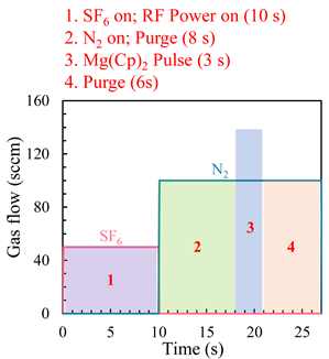
2 pulse time (3 s), nitrogen purge time (6 s), SF
6 plasma pulse time (10 s), and nitrogen purge time (8 s). The deposition temperature was varied from 100 °C to 200 °C, as listed in
Table 1.
The temperature-dependent growth mechanism for MgF
2 is proposed in
Figure 1. The relevant chemical reactions are given as Equations (1a)–(3b). The symbol s denotes substrate surface, F* represents fluorine radicals, and the symbol ↑ indicates volatile products. At 100 °C (incomplete reaction regime), the plasma energy was insufficient for complete ligand exchange, as described by Equation (1a,b). During the first half-reaction, the Mg(C
5H
5)
2 precursor reacted incompletely with the available surface –HF groups. In the second half-reaction, the fluorine radicals lack the energy to fully strip the residual C
5H
5 ligands from the surface. This might lead to a small amount of cyclopentadienyl remaining in the film. At 125 and 150 °C (ALD window), the process adhered to the ideal, self-limiting reactions shown in Equation (2a,b). The thermal energy was sufficient for every surface –HF group to react with the Mg precursor during the first pulse. The fluorine radicals were also energetic enough to completely remove every cyclopentadienyl ligand during the plasma step. This complete and sequential surface chemistry established the ideal ALD window. Above 175 °C (decomposition and CVD-like regime), the Mg(C
5H
5)
2 precursor began to undergo partial thermal decomposition on the surface (Equation (3a,b)). This created highly reactive Mg and Mg-Cp fragments that were not fully removed during the purge step. These residual species were then fluorinated during the plasma pulse, leading to growth that was no longer self-limited. The predictable consequences were a higher deposition rate, rougher and cluster-rich film morphologies characteristic of CVD-like deposition, and a loss of precise thickness control.
The refractive index and thickness of MgF2 films were determined by spectroscopic ellipsometry (M2000, J.A. Woollam Co., Inc., Lincoln, NE, USA). Measurements were performed from 300 to 800 nm at incident angles of 65°. A four-layer optical model was used to analyze the ellipsometric data (Ψ and Δ). This model included a substrate, a bulk MgF2 film layer (modeled by a Cauchy dispersion with k = 0), a Bruggeman effective medium approximation surface roughness layer (50% film material, 50% void), and an ambient air layer. The crystalline structure of the films was investigated by grazing incidence X-ray diffraction (GIXRD, Rigaku TTRAX III, Ibaraki, Japan) with Cu Kα radiation (λ = 0.15418 nm) at a fixed incidence angle (ω) of 0.5°. The scan was performed in the range of 10° ≤ 2θ ≤ 80°, with a scan rate of 1 °/min. The chemical composition and electronic states of the films were analyzed using X-ray photoelectron spectroscopy (XPS, ESCALAB 250Xi, Thermo Fisher Scientific, Waltham, MA, USA). For the XPS measurements, argon-ion sputtering was performed prior to acquisition to remove surface adventitious species (etch depth ≈ 10 nm) and minimize contamination effects. Scanning electron microscopy (SEM, Zeiss, sigma 500, Oberkochen, Germany) was used to examine the surface morphology of the films, operating at an accelerating voltage of 10 kV. An atomic force microscope (AFM, XE7, Park-Systems, Suwon, Republic of Korea) was employed to measure root-mean-square (RMS) surface roughness and surface morphologies. The optical transmittance of the MgF2 thin films deposited on glass substrates was measured using a UV-visible spectrophotometer (Lambda 850, PerkinElmer, Waltham, MA, USA) over a wavelength range of 300–800 nm. The intensity of plasma species was recorded by using an optical emission spectroscopy (OES, C210-DUVN, Xiamen Xinyifang Technology Co., Ltd., Xiamen, China).
3. Results and Discussion
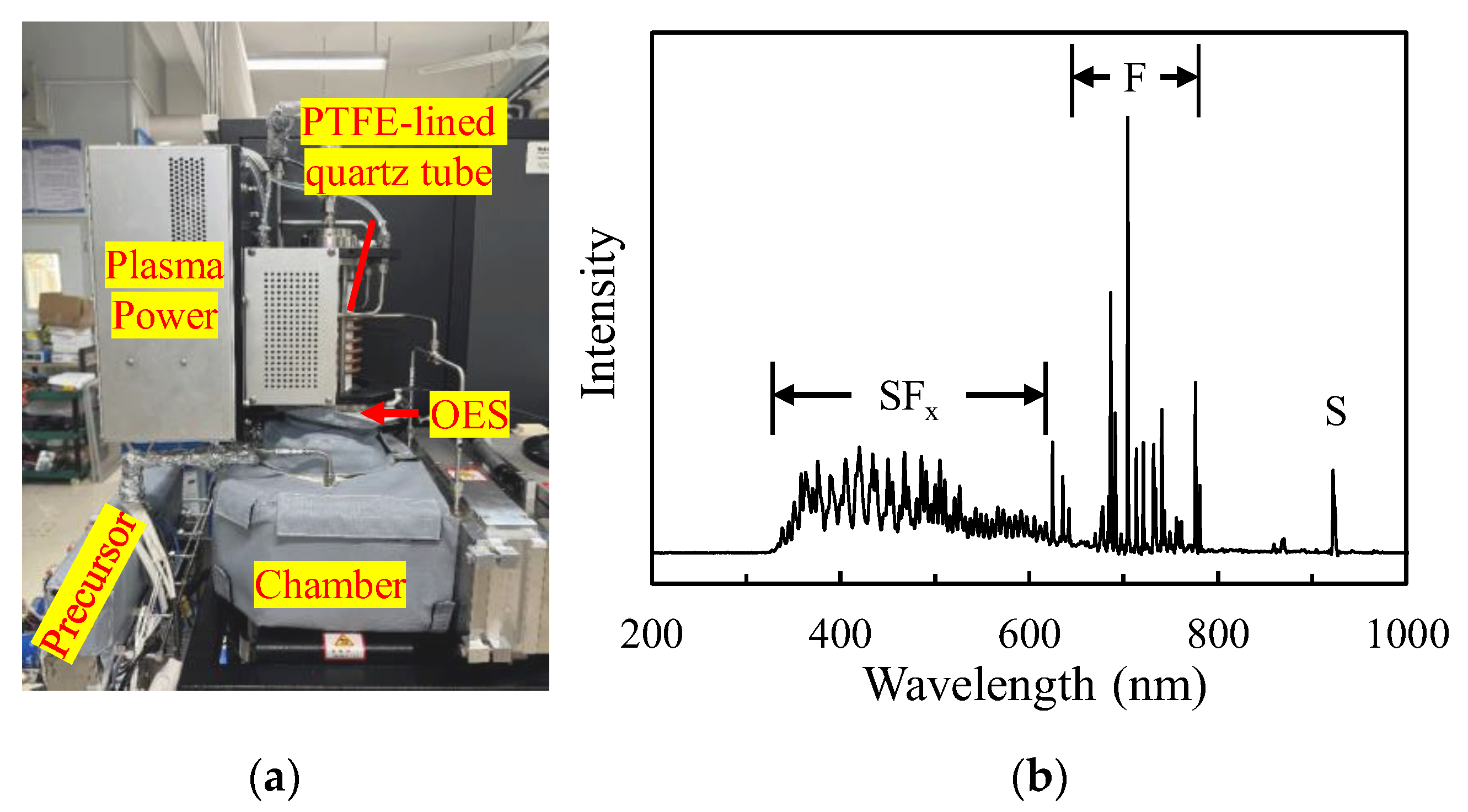
Figure 2a depicts the PEALD system used in this work. Prior studies reported unintended oxygen incorporation in PEALD-grown nitrides/fluorides, predominantly arising from plasma-induced erosion of the ICP quartz tube, which releases oxygen-containing species [
21,
22,
23]. To mitigate this, we employ a polytetrafluoroethylene (PTFE)-lined plasma quartz tube to suppress quartz erosion and the concomitant oxygen release. A corrosion-resistant dry pump is equipped to withstand F-containing by-products and prevents hydrocarbon backstreaming. Before deposition, the chamber is pre-pumped to ~1 × 10
−6 Torr using a turbomolecular pump to minimize residual O
2 and H
2O.
Figure 2b shows the OES spectrum of the SF
6 plasma. The peaks are assigned to SF
x and F* radicals according to the literature [
24,
25]. Although the sulfur-related emission lines are observed in the plasma, no sulfur is detected in the films (as will be shown later), indicating that sulfur-containing fragments do not participate in surface reactions and are removed with the exhaust. The F* radicals play a major role in the ligand exchange during the SF
6 plasma half-reaction.
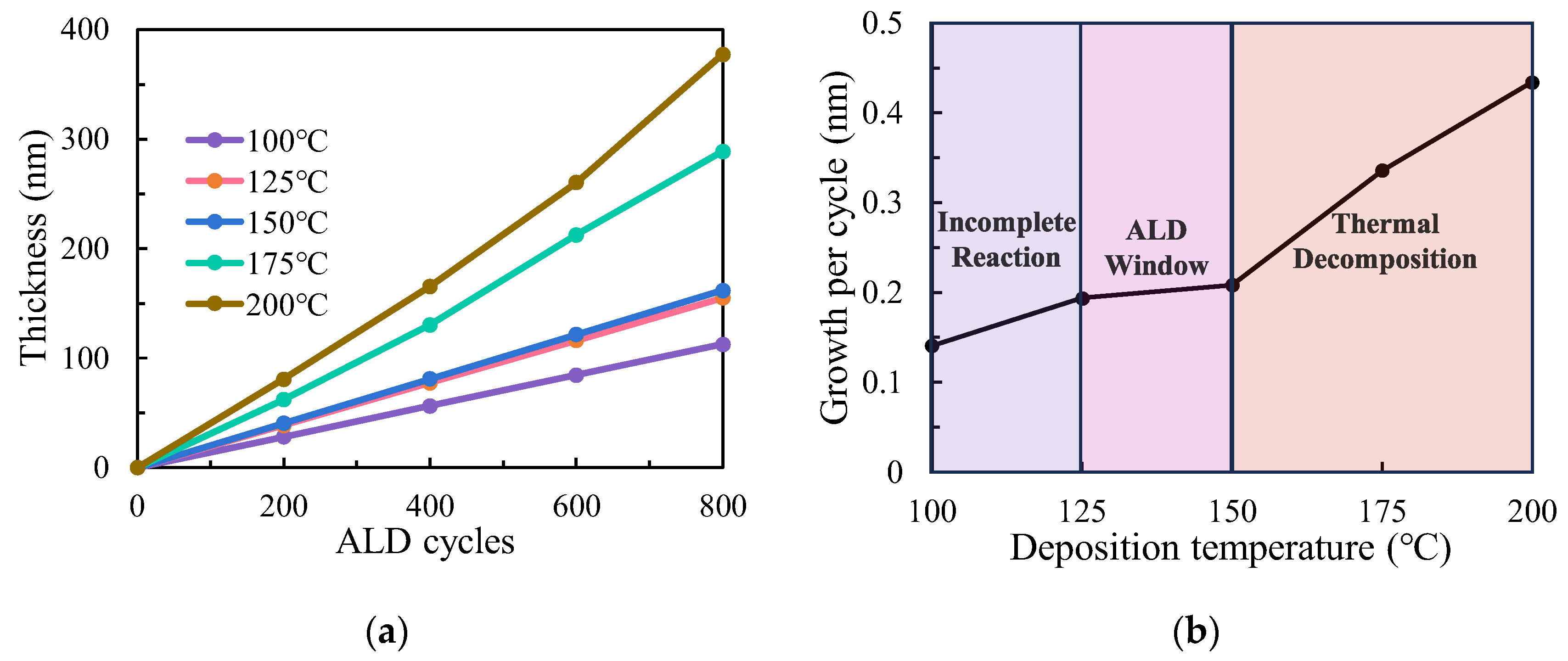
Figure 3a illustrates the relationship between the film thickness and the cycle number for MgF
2 thin films deposited at different temperatures. The thickness of films prepared at lower temperatures (≤150 °C) increases linearly with the number of cycles, indicating the self-limiting growth. While the films deposited at higher temperatures show non-linear growth, inferring they deviated from ideal PEALD behavior.
Figure 3b compiles the growth-per-cycle (GPC) versus temperature derived from linear fits of the thickness–cycle data. This GPC–temperature trend provides direct kinetic evidence for the three-regime mechanism proposed in
Figure 1. At 100 °C, the GPC is low, consistent with incomplete ligand exchange in Equation (1a,b). Within 125–150 °C, the GPC becomes temperature-insensitive at ~1.98 ± 0.05 Å cycle
−1, corroborating a self-limiting ALD window (Equation (2a,b)) and exceeding typical thermal-ALD values (~0.4–0.9 Å cycle
−1) [
16,
26]. Above 175 °C, the GPC increases sharply, indicative of a decomposition-assisted, CVD-like pathway (Equation (3a,b)). This high-temperature regime also shows increased roughness and slight off-stoichiometry, further supporting growth outside strict site-saturation.
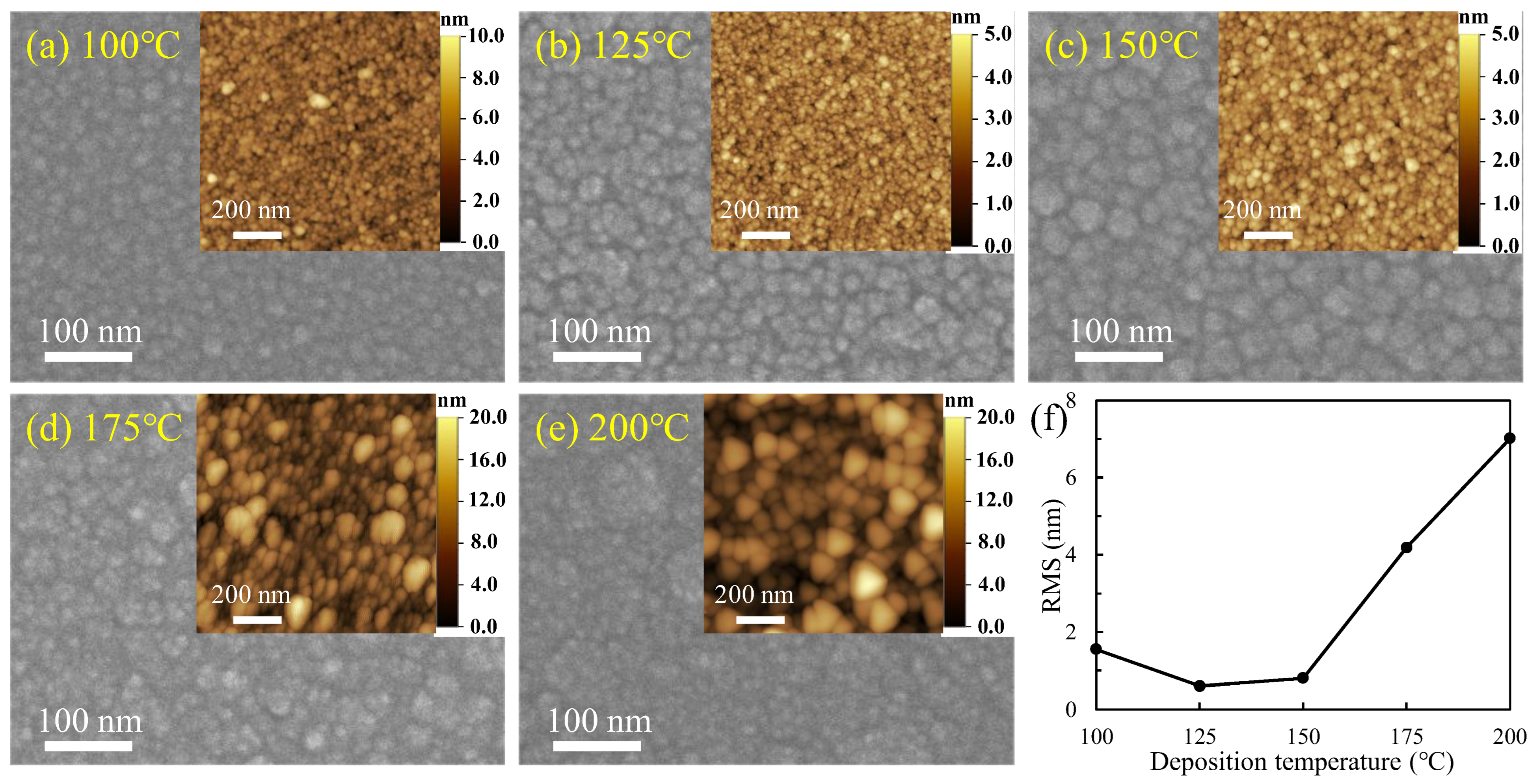
Figure 4a–e presents SEM images of MgF
2 films deposited at 100–200 °C. At 100 °C, the surface is covered with small, isolated particles and negligible clustering. When the substrate temperature is raised to 125 °C and 150 °C, the particles become large due to the enhanced surface atom migration [
27]. Further elevating the substrate temperature seems to result in smaller particles accompanied by more pronounced clustering. The AFM morphological images, as shown in the insets, reveal smooth surfaces with minimal differences among samples prepared at 100–150 °C, while higher deposition temperatures result in a noticeably rougher surface. The RMS roughness values of the films are extracted as illustrated in
Figure 4f. The RMS roughness reduces from 1.55 nm at 100 °C to 0.6–0.8 nm at 125–150 °C, then increases to 4.18 nm at 175 °C and 7.01 nm at 200 °C. The reduction at 125–150 °C reflects smoother, denser growth in the ALD window, whereas the sharp rise above 175 °C signals the transition to decomposition-assisted, CVD-like growth with particle coalescence and surface irregularity. Overall, the morphology and roughness evolution—smoothest at 125–150 °C and pronounced roughening at ≥175 °C—is consistent with the three-regime mechanism in
Figure 1.
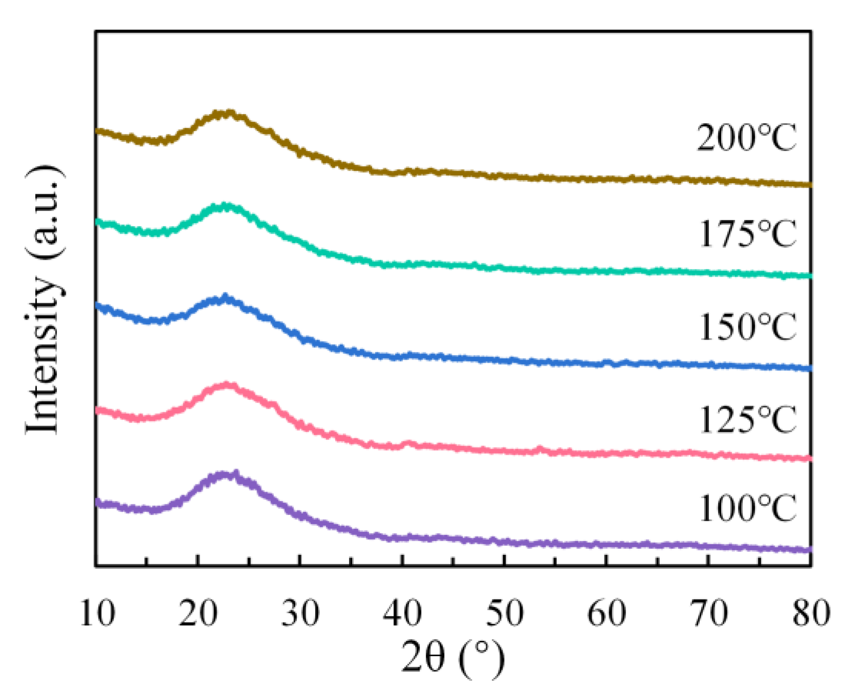
Figure 5 shows the GIXRD patterns of MgF
2 films deposited at different substrate temperatures. For all films, only a broad amorphous halo centered at approximately 20–30° (2θ) is observed and no MgF
2 Bragg reflections are present, indicating that the films are X-ray amorphous over this temperature range. An amorphous microstructure is highly desirable for visible antireflection coatings. The absence of grains and grain boundaries minimizes elastic light scattering and avoids crystallographic birefringence [
7,
28]. These characteristics directly contribute to smoother surfaces and lower scattering, which are crucial for achieving high transmittance and stable optical constants, thus benefiting AR performance. Thermal ALD typically requires high growth temperatures (≥250–300 °C) [
26,
29]. Such high temperatures frequently induce crystallization and thus negatively impacting antireflective performance. Plasma assistance in PEALD is known to enhance precursor reactivity. This generally enables lower deposition temperatures, which can in turn suppress crystallization. Therefore, the amorphous structure achieved by the PEALD MgF
2 films offers a significant advantage for high-performance antireflection coatings.
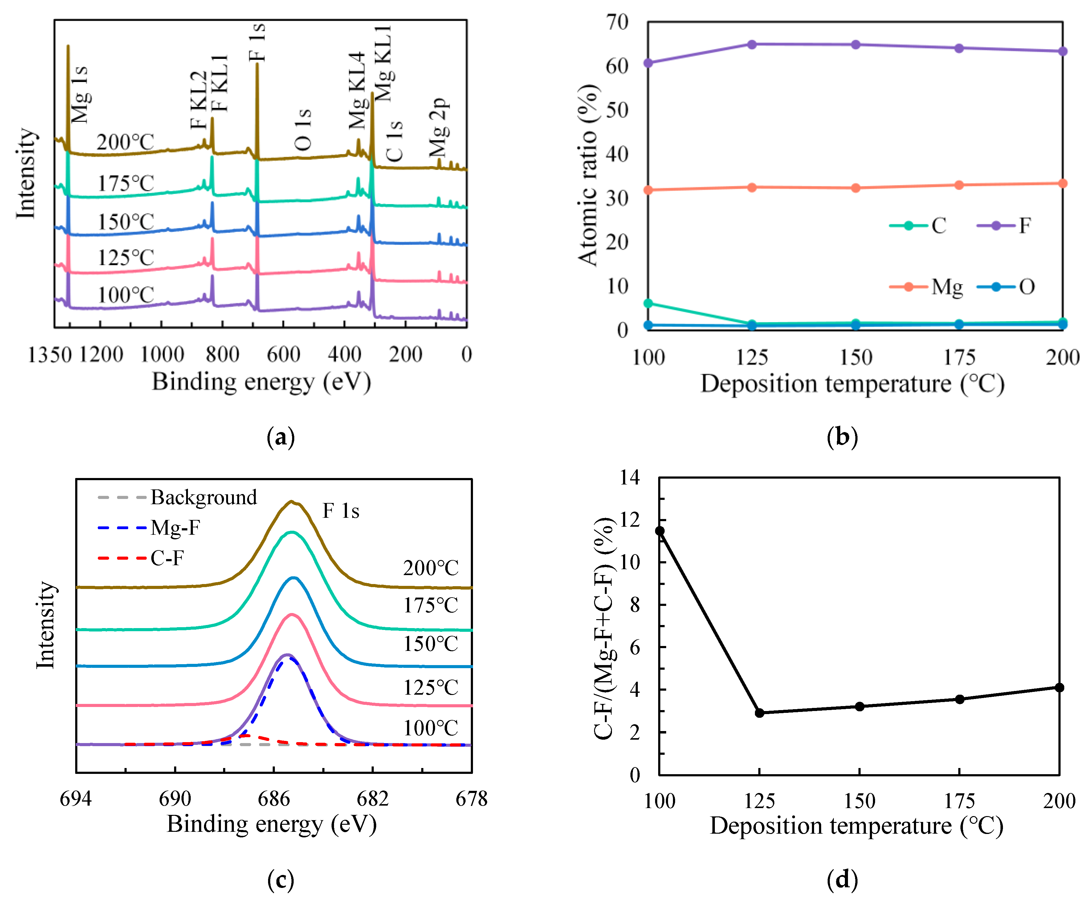
Figure 6a presents the XPS survey spectra of MgF
2 thin films deposited at various substrate temperatures. The spectra showed clear Mg and F peaks and weak C and O peaks. No sulfur was detected, indicating that sulfur-containing species observed in OES do not participate in the surface chemistry.
Figure 6b plots the atomic ratios of Mg, F, C, and O versus substrate temperature. The 100 °C sample has a significantly higher carbon content than other samples, attributed to insufficient energy to completely remove organic components of the metal precursor during the surface ligand exchange process. The oxygen content stays below 1.5 at.% for all films, reflecting the effectiveness of the PTFE-lined ICP tube and the high-vacuum pre-pump in suppressing oxygen incorporation. In comparison, the films prepared with an unlined plasma tube under identical conditions exhibit a significantly higher oxygen content of 6.2 at.%. Correspondingly, the F:Mg ratio also improves from 1.72 (unlined) to 1.92 (PTFE-lined).
Figure 6c depicts the F 1s core-level spectra of the films. The deconvolution (shown for the 100 °C sample as representative) yields two components at ~685 eV and 688.5 eV, assigned to Mg–F and C-F, respectively [
30,
31]. The area ratios of C-F component to the total are plotted in
Figure 6d. The trend of C-F peak area ratio is similar to that of carbon content, suggesting that the elevated carbon at 100 °C originates from incomplete ligand removal during unsaturated low-temperature half-reactions. Deposition temperature is therefore a key variable for controlling film purity and stoichiometry. These compositional trends align with the mechanism in
Figure 1: at 100 °C, incomplete reactions leave residual C/C-F; at 125–150 °C, self-limiting half-reactions minimize impurities and stabilize stoichiometry; and at ≥175 °C, slight deviations are consistent with decomposition-assisted growth.
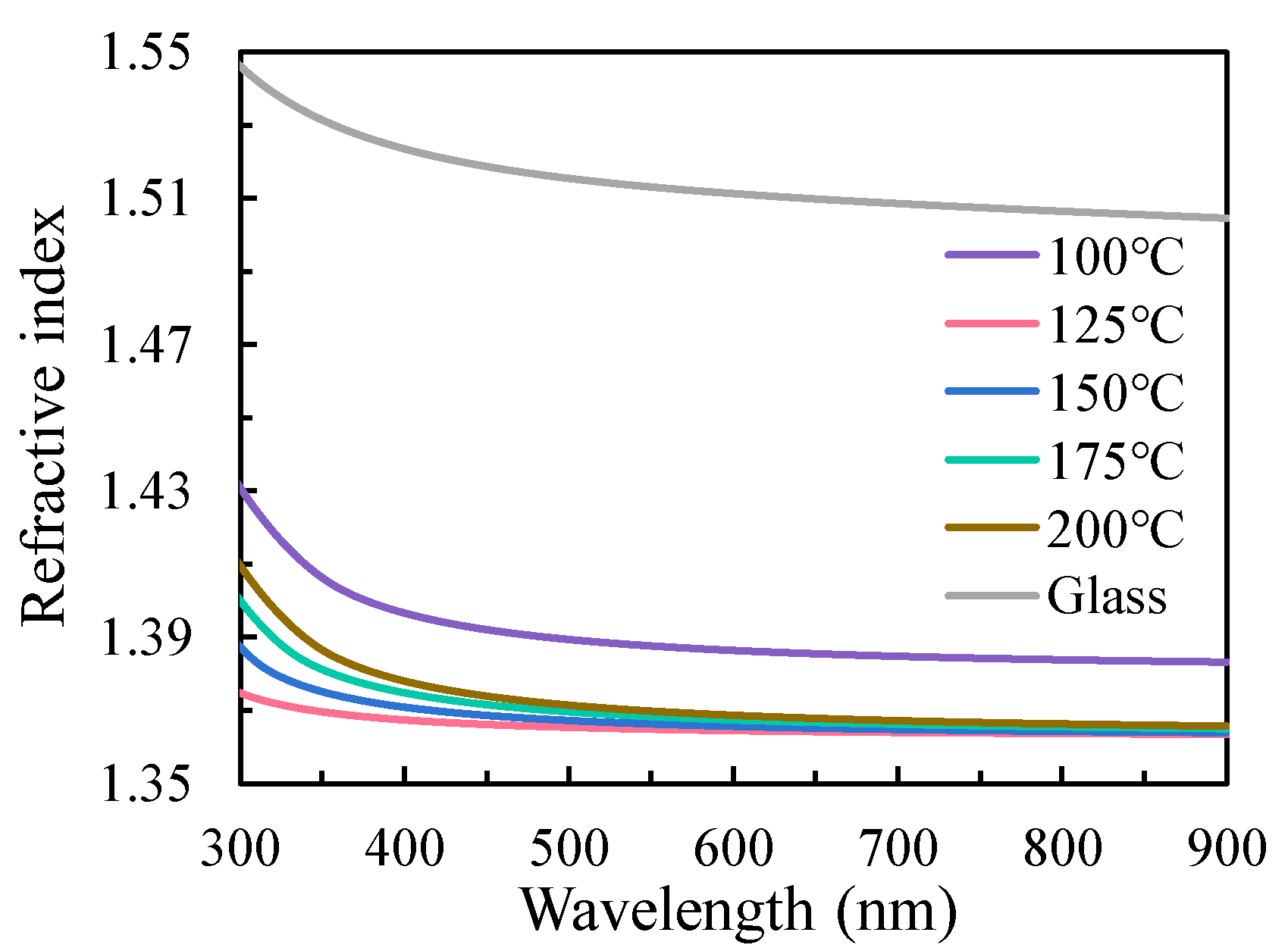
Figure 7 displays the refractive index spectra of MgF
2 films grown at 100–200 °C together with the bare-glass reference. It is observed that the curves of all coated samples remain remarkably lower than that of bare glass across the spectrum, enabling the antireflection function. Using the refractive index at 550 nm for comparison, the film deposited at 100 °C exhibits the highest value, whereas that prepared at 125 °C reaches a minimum of 1.37 ± 0.003, matching the value reported for ideal bulk MgF
2 [
32,
33]. This low refractive index contrasts sharply with the 1.49 observed for films prepared using an unlined tube under identical conditions. The 150–200 °C curves nearly overlap but with a slight upward trend, indicating that any further densification beyond the ALD window is marginal. The refractive index reaches its minimum at 125 °C, where the film is near-stoichiometric MgF
2 and carbon is lowest (XPS C ≈ 1.46 at%), minimizing electronic polarizability. At 150 °C, although still within the ALD window, the refractive index increases slightly, consistent with a small rise in carbon (≈1.64 at%) and marginally tighter packing. From 175 to 200 °C, the XPS result shows a mild F deficiency, which increases the average electronic polarizability and further contributes to the rise in n. By contrast, at 125 °C the index reaches a minimum because self-limited growth yields near-stoichiometric MgF
2 with the lowest carbon level. Overall, the index evolution—high at 100 °C, a minimum within 125–150 °C, and a rise at ≥175 °C—aligns with the three-regime mechanism: incomplete low-temperature reactions leave residual organics (higher n); self-limiting chemistry in the ALD window yields low-n films; and decomposition-assisted growth at high temperature introduces off-stoichiometry that elevates n.
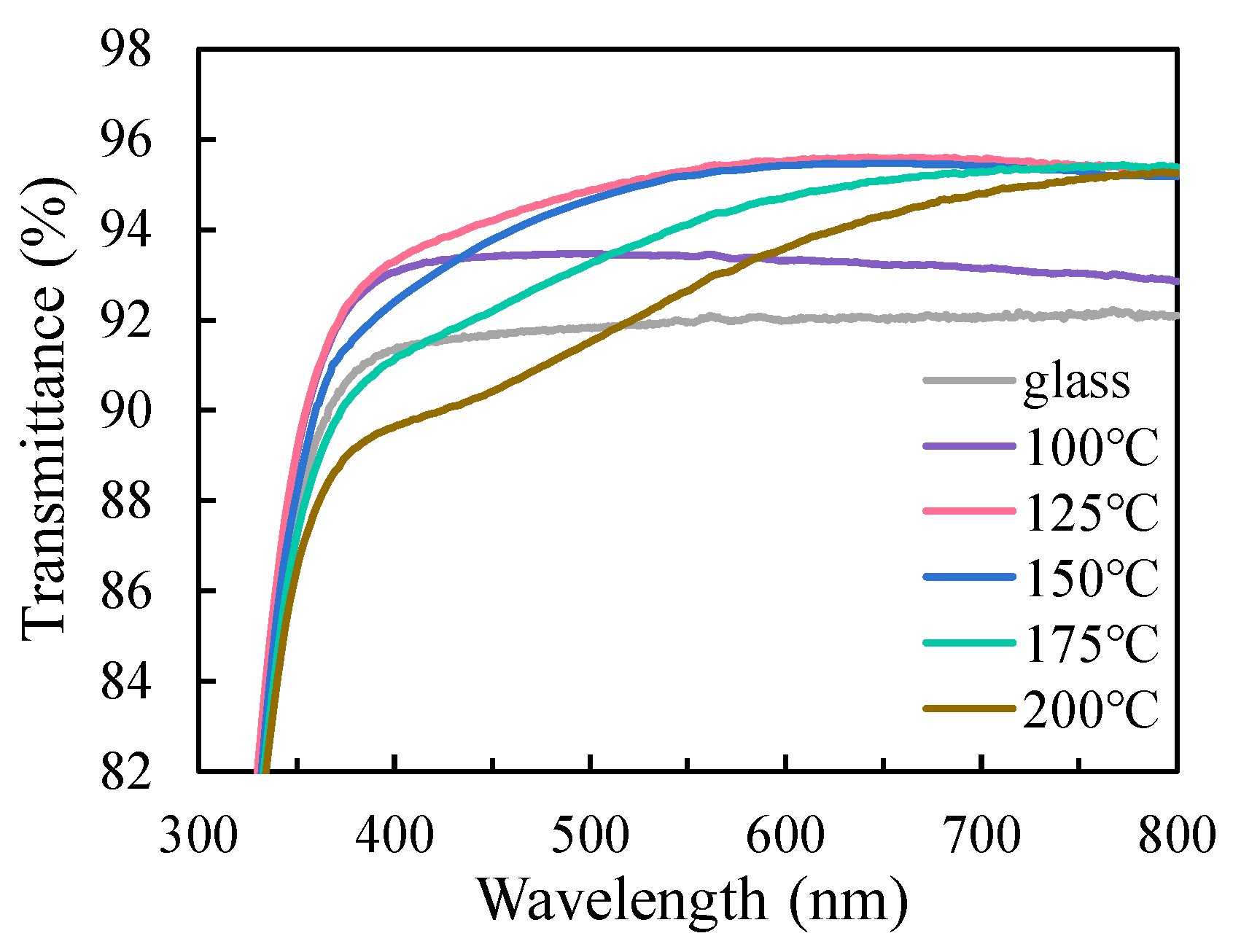
Figure 8 compares the transmittance spectra of glass without and with the films deposited at different substrate temperatures. The transmittance increases with deposition temperature and reaches a maximum at 125 °C, then declines at higher temperatures. The process temperature also dictated the film’s final thickness, which was measured to be 56, 78, 81, 130, and 166 nm for deposition temperatures of 100, 125, 150, 175, and 200 °C, respectively. These physical thickness variations, coupled with changes in refractive index (n), alter the optical path length (n × d, where d is the physical thickness) of the film. The red shift in the interference maxima in the transmittance spectra corresponds directly to the increase in optical path length. This follows the relationship for a quarter-wave antireflection coating, where the maximum transmittance wavelength is approximately 4nd. While the spectral positions of these maxima are thickness-dependent, their peak magnitudes provide a direct indication of the intrinsic antireflection quality and material purity of the films. Considering the overall anti-reflection performance, the 125 °C film achieves the optimal balance, having the lowest refractive index and the smoothest surface (0.6 nm RMS). This combination leads to the highest peak transmittance, approximately 95.4 ± 0.2%, and the best overall antireflective performance. At 150 °C, the refractive index slightly rises, while roughness remains low at 0.8 nm, with peak transmittance still high, around 95 ± 0.2%. However, at 175 °C and 200 °C, both the refractive index gradually increases (1.38) and the RMS roughness sharply rises (4.2–7.0 nm). These factors degrade antireflective properties. Although peak transmittance can still reach around 95.0 ± 0.2%, the significantly increased roughness causes greater light scattering, which distorts the spectral shape. Therefore, the film deposited at 125 °C is identified as optimal. It minimizes both reflective and scattering losses due to its ideal refractive index and smoothest surface morphology.
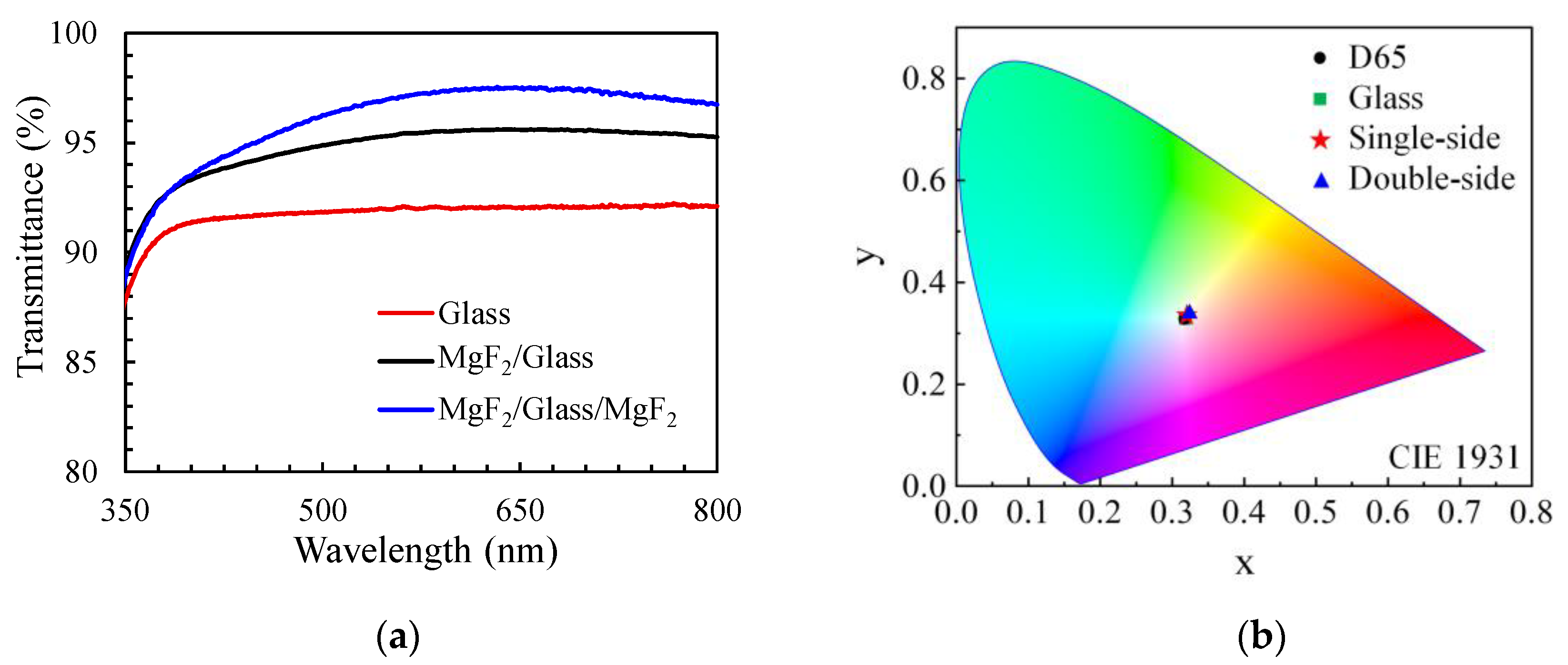
To further enhance the transmittance of glass, the optimal MgF
2 film (deposited at 125 °C) was coated on both sides.
Figure 9a compares the broadband transmittance of bare glass with substrates bearing single-sided and double-sided MgF
2 coatings. The single-sided coating improves transmittance from 92.0 ± 0.1% (bare) to 95.4 ± 0.2% at 550 nm. For double-sided coatings, the transmission reaches 97.2 ± 0.2% at 550 nm, with an average visible transmittance (380–780 nm) of 96.4 ± 0.2% (compared to 93.8 ± 0.2% for single-sided). As transmission below ~350 nm is limited by the glass substrate, the analysis focuses on the visible band. In addition,
Figure 9b plots the transmitted chromaticity (CIE 1931 (x, y), 2°/D65) for bare glass, single-sided, and double-sided coated samples.
Table 2 reports comprehensive color specifications. It includes CIE 1931 (x, y) coordinates and CIE 1976 (L*, a*, b*) color parameters. L* represents lightness, a* indicates the red-green chromaticity, and b* indicates the yellow-blue chromaticity. ΔE
ab quantifies the total color difference within this CIE 1976 space, calculated for each coating relative to bare glass. The coatings lie close to the D65 white point. The ΔE
ab is approximately 1.43 for single-sided coatings and 2.24 for double-sided coatings. These low color differences are highly desirable, ensuring excellent visual clarity and color fidelity for optical applications.
Table 3 compares MgF
2 thin film properties achieved by PEALD in this work and other deposition methods. Thermal ALD typically operates at much higher temperatures (350 °C). This yields polycrystalline films with significantly higher roughness (6.3–7.1 nm), despite achieving similar refractive indices. Such high-temperature growth, which leads to increased roughness and compositional deviations, inherently restricts the practical use of these films in high-performance optical systems. E-beam evaporation can produce amorphous films with low roughness (0.56 nm) but at a higher deposition temperature (240 °C). Sputtering can deposit films at room temperature. However, it tends to produce nanocrystalline or polycrystalline structures and results in higher roughness (12 nm). The PEALD approach in this work thus integrates a low deposition temperature, amorphous microstructure, low refractive index, and exceptionally low surface roughness simultaneously. This combination results in high transmittance, surpassing values achieved by other methods.

