Article

Exploring the Optoelectronic Properties and Solar Cell Performance of Cs2SnI6−xBrx Lead-Free Double Perovskites: Combined DFT and SCAPS Simulation

1
Laboratory of Quantum Physics of Matter and Mathematical Modeling (LPQ3M), University Mustapha Stambouli of Mascara, Mascara 29000, Algeria
2
Laboratoire de Physique de la Matière Condensée, Département de Physique, Faculté des Sciences de Tunis, Université Tunis El Manar, Tunis 2092, Tunisia
3
Electrical Engineering Department, Future University in Egypt, Cairo 11835, Egypt
4
Department of Measurements and Control Systems, Silesian University of Technology, 44-100 Gliwice, Poland
5
Faculty of Engineering, Ain Shams University, Cairo 11517, Egypt
6
Department of Chemistry, College of Sciences, King Saud University, P.O. Box 2455, Riyadh 11451, Saudi Arabia
7
Center of Nanoelectronics and Devices, The American University in Cairo, Cairo 11835, Egypt
*
Author to whom correspondence should be addressed.
Submission received: 12 October 2024 / Revised: 23 November 2024 / Accepted: 30 November 2024 / Published: 17 January 2025
(This article belongs to the Section Applied Physics)

Abstract

:
This paper presents detailed results regarding the physical behavior of Cs2SnI6−xBrx alloys for their potential use in photovoltaic applications. Numerical computations based on density functional theory (DFT) revealed that Br substitution at I sites significantly influenced the electronic structure of Cs2SnI6, resulting in an increase in bandgap values from 1.33 eV to 2.24 eV. Additionally, we analyzed the optical properties, including the absorption coefficient, which exhibited high values in the visible light region, highlighting the material’s excellent light-trapping abilities. Moreover, Cs2SnI6−xBrx compounds were employed as absorber materials in an fluorine-doped tin oxide (FTO) TiO2/Cs2SnI6/P3HT/Ag perovskite solar cell (PSC) to investigate its performance. The simulation process consisted of two interconnected steps: (i) the DFT calculations to derive the material properties and (ii) the SCAPS–1D (one-dimensional (1D) solar cell capacity simulator) simulation to model device performance. To ensure reliability, the SCAPS–1D simulation was calibrated against experimental data. Following this, Cs2SnI6−xBrx compound with various ratios of Br content, ranging from 0 to 6, was investigated to propose an efficient solar cell design. Furthermore, the cell structure was optimized, resulting in a development in the power conversion efficiency (PCE) from 0.47% to 3.07%.

1. Introduction

Photovoltaic (PV) technologies stand out as one of the most efficient renewable energy sources available [1]. Due to their advantageous optical and electronic properties for use in field-effect transistors, light-emitting diodes, and effective PV devices, materials research into perovskites has rapidly expanded over the past few years [2,3,4,5,6]. Lead halide-based perovskites such as APbX3, where A denotes the cation and X denotes the anion, have been considered as the best materials for photovoltaic applications with power conversion efficiencies (PCEs) above 25% [7]. However, APbX3n has two bottleneck problems, namely toxicity and instability, which must be addressed before its full commercialization [8,9,10,11,12]. To prevent toxic Pb, another group-IV element, tin (Sn), with low toxicity and physical properties, similar to Pb, has emerged as a potential candidate [13,14,15,16]. Unfortunately, the alternate ASnX3 perovskite materials have shown poorer performance than APbX3 [17]. The susceptibility to moisture and light seen in the ASnX3 compound is exacerbated by the ease with which Sn2+ can be oxidized to Sn4+.
Recently, tetravalent metal compounds such as A2MX6 adopting the K2PtCl6 structure type [18] with a space group of Fm3m have drawn interest as innovative candidates for replacing lead-based ABX3 perovskite materials [19,20,21,22,23,24,25,26,27,28], where M and B denote cations of different sizes and generally M atoms are smaller than B atoms, and B atoms are smaller than A atoms. Among these groups, vacancy-ordered Cs2SnX6 compounds have recently gained much attention due to their direct band gap nature, high absorption, and excellent durability [29,30,31,32,33]. In particular, Cs2SnI6 is exploited as a light absorber in solar cells (SCs) and reveals a maximum PCE of about 1% [34]. Furthermore, using Cs2SnI6 as a hole transporting material has been shown to enhance the performance of SCs based on N719, YD2-o-C8, and RLC5 dyes by 7.8% [35]. However, despite possessing feasible photoelectric properties, the performance of Cs2SnI6-based SCs appears to be inferior when compared to Pb-based perovskites. The poor performance of SCs is noticeable due to the dominant VI and Sni defects and the unbalanced carrier mobility [29,36].
Recent investigations on solar cells based on CH3NH3PbX3 (X = Cl, Br, I) have established that the perovskites’ performance is closely linked to the type of halogen anion and it is possible to adjust their optoelectronic characteristics by blending various halogens [37]. Thus, a comparable response can be anticipated when it comes to Cs2SnX6. According to the studies in Refs. [38,39], Cs2SnI6−xBrx materials have a tunable band gap and excellent thermal stability, making them ideal for SC applications. In the study [38], efficient Cs2SnI6−xBrx thin films were fabricated by optimizing the iodine-to-bromine ratio. Using a device structure comprising FTO/TiO2/Sn-TiO2/Cs2SnI4Br2/Cs2SnI6/LPAH/FTO, where FTO denotes fluorine-doped tin oxide, a PCE of 2.025% was achieved. The device also demonstrated enhanced stability, outperforming Cs2SnI6-based perovskite solar cells [38]. Furthermore, In the study [40] a straightforward hydrothermal method was developed to synthesize high-quality Cs2SnX6 (X = Br, I) crystals. These vacancy-ordered perovskites feature bandgaps of 1.84 eV (Cs2SnI6) and 1.42 eV (Cs2SnBr6). In Ref. [41], the authors introduced a one-step synthesis of high-quality Cs2SnI6−xBrx perovskite using methanol, enhancing the material stability and utilization and achieving an efficiency of 3.2%.
Additionally, from a theoretical perspective, it is well established that substituting I atoms with Br or chlorine Cl in Cs2SnI6 perovskite significantly alters its optoelectronic properties, potentially enhancing its PV performance [42,43,44]. Shihui Guo and collaborators [44] e explored the influences of Cl/Br doping on the stability and optoelectronic properties of Cs2SnI6, revealing improved structural and electronic characteristics that highlight its potential in optoelectronic applications. In their theoretical study, three double perovskites, Cs2SnI4Cl2, Cs2SnI4ClBr, and Cs2SnI4Br2, were comprehensively investigated utilizing the density functional theory (DFT), with computed bandgaps of 1.75, 1.75, and 1.56 eV, respectively [44]. Jin Zhang and collaborators [43] provided an in-depth analysis of optical absorption properties of Cs2SnI6−xBrx (x = 0–6). The bandgap values for different x compositions were calculated with the HSE06 hybrid functional. Bandgaps ranging from 1.27 eV (for x = 0) to 2.75 eV (for x = 6) were recorded. The study [43] also demonstrated that Br ion doping not only adjusts the optical bandgap but also enhances stability, paving the way for efficient lead-free PV applications. Moreover, it has been reported that doping Cs2SnI6 with tellurium (Te) also results in significant modifications to its electronic properties. Specifically, Te-doped Cs2SnI6, forming Cs2Sn1−xTexI6 (where x = 0, 0.25), demonstrated a consistent increase in the band gap from 1.20 eV to 1.40 eV as the composition x rises [42]. This tunability of the bandgap not only improves material stability but also renders it a promising candidate for optoelectronic device applications.
Notably, understanding the fundamental properties of mixed Cs2SnI6−xBrx can establish its potential application in perovskite solar cells. This encourages us to conduct additional research into the structural, electronic, and optical properties of a Pb-free Cs2SnI6−xBrx solid solution. Thus, in the present study, the Cs2SnI6−xBrx perovskite compound is thoroughly explored. The structural and electronic properties, density of states, effective masses, and optical properties of the proposed perovskite compound are analyzed. The potential application of the perovskite compound in solar cells is explored, and a solar cell prototype incorporating the compound is developed utilizing SCAPS device simulations. The derived DFT material properties are used as the input to SCAPS to model the device performance. To validate the accuracy of the simulation model, the performance of the proposed solar cell is calibrated against the experimental data. Subsequently, optimization techniques are employed to enhance the efficiency of the calibrated PV cell.
The rest of this paper is consolidated as follows. The details of the DFT calculations for the material study and solar cell simulations are presented in Section 2. Cs2SnI6−xBrx properties and its solar cell applications are illustrated and discussed in Section 3. Section 4 concludes our work.

2. Details of Calculations

2.1. Material Study

We conducted all calculations ab initio by employing the full potential linearized augmented plane wave (FP–LAPW) approach [45], as employed in the WIEN2k software package [46]. The Wu–Cohen generalized gradients approximation (GGA–WC) functional was employed to describe the exchange–correlation interactions and verify optimized structural parameters, including lattice dimensions and atomic positions. To calculate the electronic structure, we utilized the Tran and Blaha modified Becke–Johnson (TB–mBJ) potential [47], specifically designed to yield a bandgap value closer to the experimental measurements than the standard GGA.
To ensure precise calculations, several convergence parameters needed careful adjustment, namely Kmax (the maximum wave vector), R MT min (the smallest muffin-tin (MT) sphere radius), ℓmax (angular momentum cut-off), RMT (muffin-tin radii) for Cs, Sn, Br, and I, and the number of k-points in the irreducible Brillouin zone (IBZ). We chose the following values for convergence: R MT min K max = 8, RMT(Cs) = 2.5a.u. RMT(Sn) = 2.41a.u., RMT(Br) = 2.25a.u., RMT(I) = 2.45a.u., max = 10, and 125 k-points in the IBZ. The crystal structure was engineered by minimizing the forces applied to each constituent atom, with a total energy convergence criterion set at 10−4 Ryd.

2.2. SCAPS–1D

The one-dimensional (1D) SCAPS–1D software has been realized for its capability to simulate various types of perovskite solar cells and other thin-film solar devices, having been extensively utilized and validated against experimental investigations [7,28]. It operates by solving fundamental physical equations, namely the continuity equations (S1) and (S2) and Poisson’s equation (S3), ensuring self-consistency before convergence is achieved. (see the Supplementary Materials). Table S1 provides an overview of the physical and technological parameters involved in the mentioned equations. The rate of solar-induced carrier generation, G(x), varies with the depth below the semiconductor surface subjected to incident light, as defined by (S4). The solution methodology employed by SCAPS–1D is depicted in Figure S1, involving sequential steps such as defining cell geometry and incorporating material parameters. The finite difference method (FDM) is utilized for approximation, with the Scharfetter–Gummel technique employed to model the current densities [38]. This technique iteratively computes the electron and hole concentrations (n and p) at grid points [39]. Through successive iterations, physical quantities such as the electrostatic potential (U) and solar-induced carrier generation (G) are refined. Finally, various characteristics including current density–voltage (JV) curves, capacitance–voltage (CV) profiles, capacitance–frequency (CF) responses, and external quantum efficiency (QE) can be studied. Other physical quantities can also be extracted such as the generation rate (G), recombination rate (U), and energy band diagrams [48].
A flowchart representing the computation/simulation mechanism in this research activity is provided in Figure 1. The flowchart highlights the methodology, integrating DFT calculations with SCAPS simulations to optimize the operation of perovskite solar cells (PSCs) under investigation. Firstly, the process is initiated with the execution of DFT calculations, aimed at obtaining critical electronic and optical properties of Cs2SnI6−xBrx perovskites for different Br contents. These calculations comprise the determination of structural parameters, electronic band structures, density of states, effective masses, and optical properties such as the absorption coefficient and bandgap energies. Subsequently, building upon the insights gathered from the DFT calculations, the methodology progresses to perform SCAPS simulations. These simulations are anchored in experimental studies, leveraging the calibration of a comparable solar cell structure to validate the models employed. Following validation, the simulations entail the development of PSC designs, incorporating Cs2SnI6−xBrx as an absorber layer. Throughout the simulation process, key parameters including the Br content, absorber doping concentration and thickness, carrier transport materials (electron and hole transport layers (ETLs and HTLs)), and bulk defects are meticulously analyzed and optimized.

3. Results and Discussions

3.1. Material Properties

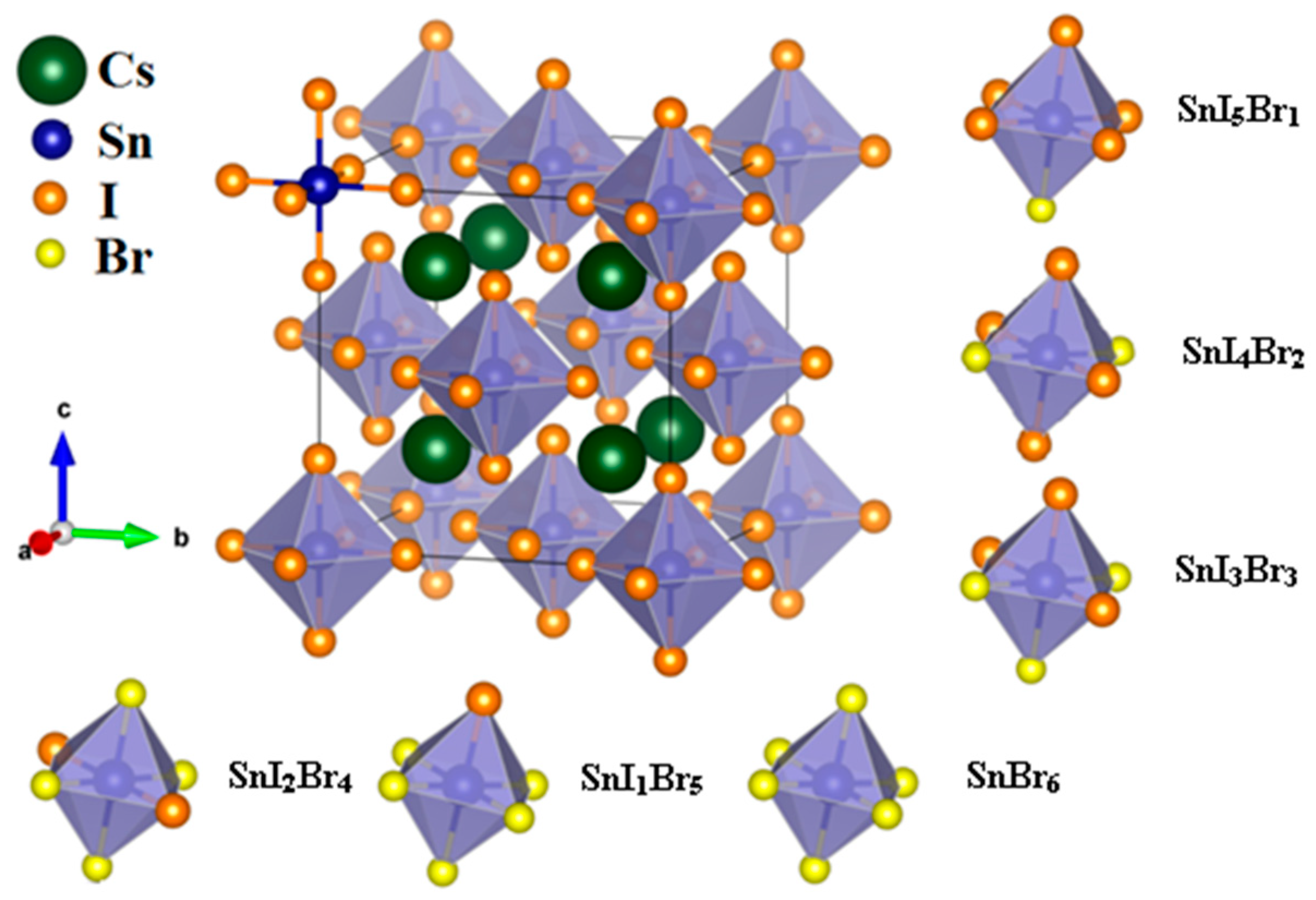
3.1.1. Structural Properties

Cs2SnI6 crystalizes in the cubic Fm3m space group (225). There are four formula units per unit cell, leading to 36 atoms in the primitive unit cell. Figure 2 shows the crystal structure of Cs2SnI6−xBrx for x = 0, 1, 2, 3, 4, 5, and 6. The optimized lattice parameters of Cs2SnI6−xBrx for different concentrations are recorded in Table 1 with other available theoretical and experimental data. The GGA–WC approximation was used to carry out structural parameter optimization. On optimization of Cs2SnI6−xBrx, the lattice parameter a decreases as x increases, as can be deduced from Table 1. This result is predictable because the ionic radius of the Br ions (0.196 nm) is smaller than that of the I ions (0.220 nm).

3.1.2. Electronic Properties

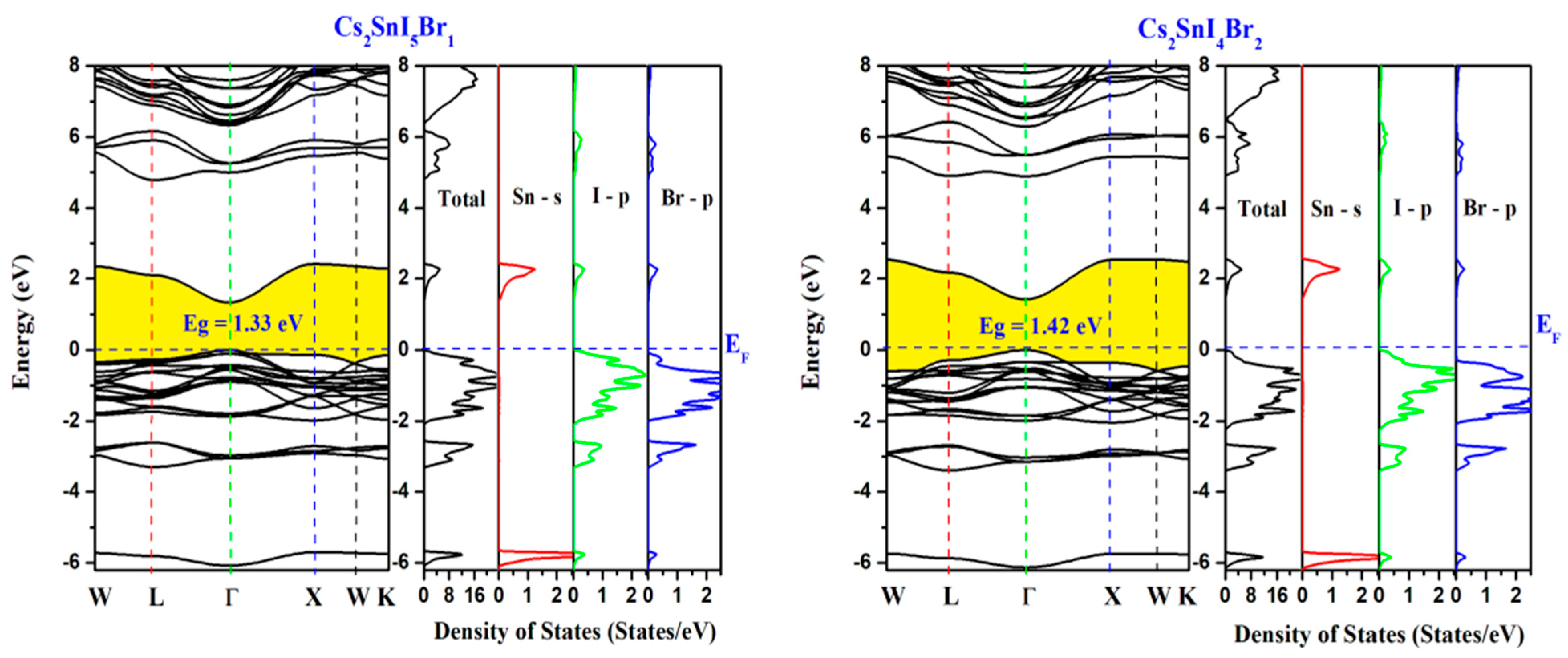
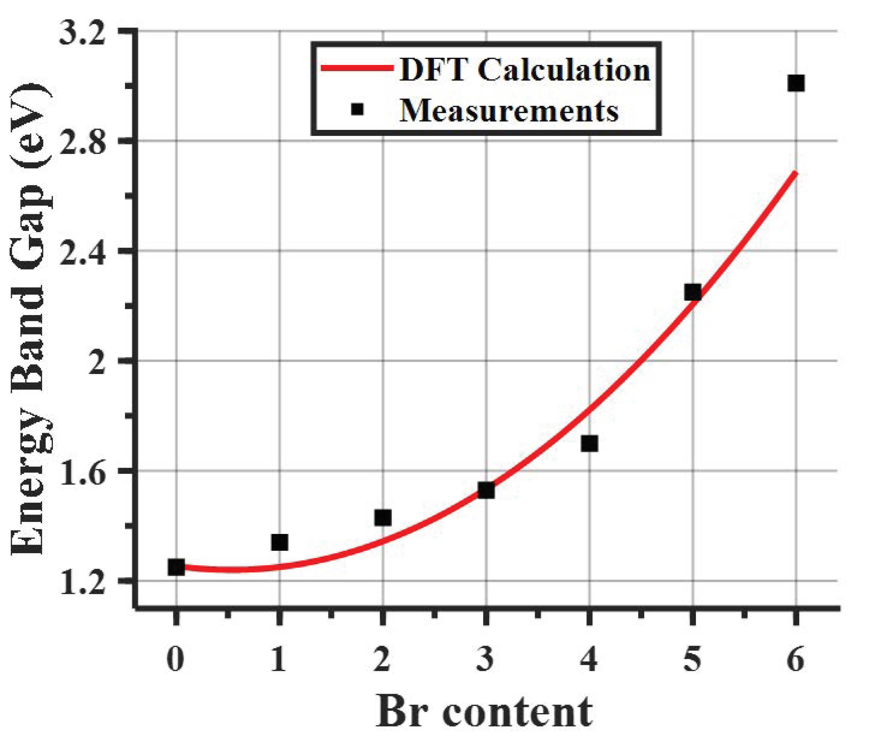
Electronic Band Structure and Densities of States

Using the GGA–WC and mBJ functionals, the energy bands of the end compounds (x = 0 and 6) were first determined. Their computed band structures are shown in Figure 3, which reveals that Cs2SnI6 and Cs2SnBr6 are direct band gap semiconductors with values of 1.257 eV and 2.69 eV, respectively, using the mBJ functional localized at the Γ point. For x = 0, Figure 3a shows that Cs2SnI6 has an intermediate band (IB), despite the fact that according to TB–mBJ calculations a second band from the valence band (VB) maximum extends to 4.48 eV, reaching the conduction band (CB) minimum. According to Ref. [52], cells indicating the VB to IB and IB to CB transitions are two cells in the series, while the VB to CB transition is a parallel cell. Figure 4 displays the computed band structures and densities of states for the other values of x (x = 1, 2, 3, 4, and 5). Regarding Figure 4, one observes that the energy of the intermediate band rises as the Br content x rises. The calculation of the energy band structure for the remaining Cs2SnI6−xBrx structures for x = 2, 3, 4, and 5 is based on TB–mBJ potential, which displays a direct energy gap spanning from 1.33 eV to 2.24 eV, shown in Table 2. As can be seen from Table 2, the band gap in Cs2SnI6−xBrx increases when Br atoms are substituted in the I site. As can be deduced from Table 2, the computed band gap (Eg) values using the TB–mBJ approximation are the closest to the experimental results.
Moreover, Figure 5 depicts the variation of Eg with the Br composition. The band gap trend follows a nonlinear dependency on the Br content. This behavior can be attributed to the difference in atomic properties between iodine and bromine, particularly their atomic sizes and electronic structures. Bromine has a smaller atomic radius and higher electronegativity compared to iodine, leading to a stronger localization of electrons and a widening of the electronic band gap. As the Br composition increases, the conduction and valence band edges are influenced, resulting in a shift of the band gap towards higher energy values. It can be inferred from the figure that our DFT calculations are in reasonable agreement with previous experimental investigations [39].
Using the following equation, the optical bowing parameter b [56] was determined to find the relationship between the Eg and the Br composition x:
        E g C s 2 S n I 6 x B r x = x 6 E g C s 2 S n B r 6 + 1 x 6 E g C s 2 S n I 6 b x 1 x 6 ,
where E g C s 2 S n B r 6 and E g C s 2 S n I 6 are the band gap of the end compounds for x = 6 and x = 0, respectively. The dependence of the calculated E g on the Brx content can be determined by fitting the variation with a quadratic function, as follows:
E g C s 2 S n I 6 x B r x = 1.254 + x 0.239 b + b 6 x 2 .
The computed bowing parameter b is 0.291. From the calculated density of states (DOS), the top of the VBs ranging from −3 eV to 0 eV are formed primarily from the p orbitals of the I (Br) atoms. The IB minimum is essentially derived from the s-orbital Sn-s bands, while the bottom of the CBs is formed mostly by the hybridized S-s and I (Br)-p bands.

Effective Masses

Calculating the carrier effective masses is frequently desirable to analyze the power efficiency of photovoltaic materials and for a detailed search of energy states in PV cells. The effective masses are obtained by fitting parabolic dispersion curves to our energy band structures [57,58]. The computed effective masses of Cs2SnI6−xBrx alloys are given in Table 2 along with earlier theoretical and experimental information. It is observed that holes are heavier than electrons in all structures. This obtained result can be explained by the fact that the VB originates from unhybridized I (Br)-p orbitals, which are less dispersed compared to the CB, which is formed by antibonding states of I (Br) anions and Sn cations.

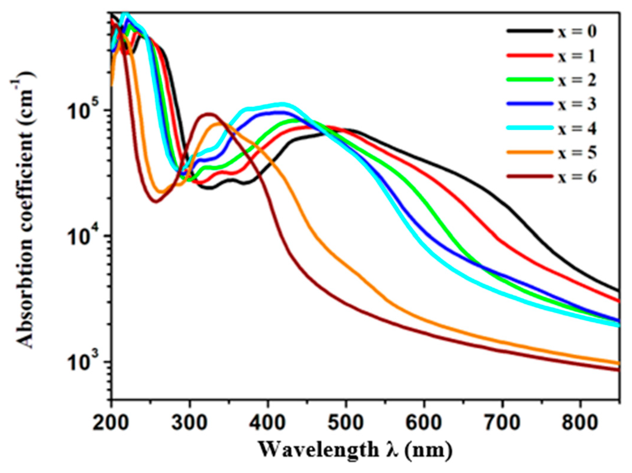
3.1.3. Optical Properties

The frequency dependent dielectric function is used to determine the optical properties of solids and is given as   ε ω = ε 1 ω + i ε 2 ω , where ε 1 ω and ε 2 ω stand for the real and imaginary parts of   ε ω , which correspond to the material’s dispersive and absorption behaviors, respectively, and ω is the photon energy. Figure 6a,b shows the results of the ε 1 ω   and   ε 2 ω spectra for Cs2SnI6−xBrx with variations in photon energy, respectively. The static dielectric constant ε 1 0 for Cs2SnI6−xBrx is 3.86, 3.85, 3.84, 3.77, 3.24 and 3.15 for x = 0, 1, 2, 3, 4, 5 and 6 and are reported in Table 3, which shows that the addition of the Br atoms reduced   ε 1 0 . Thus, Cs2SnI6−xBrx becomes less conducting at low frequency when x increases. To evaluate the stability of excitons, the exciton binding energy is computed using the Bohr model, which is given as [59]:
E b = 13.6   e V · μ * ε 0 .
With ε 0 denotes the static dielectric constant and μ * is the reduced mass. Table 3 also summarizes the computed E b for Cs2SnI6−xBrx for x = 0, 1, 2, 3, 4, 5 and 6. The results for Eb show that the exciton binding energy increases as x increases in Cs2SnI6−xBrx.
The zeros of ε 1 ω that correspond to the frequencies of screened plasma are positioned at 9.75 eV, 9.91 eV, 10.10 eV, 10.19 eV, 10.76 eV, 14.84 eV and 15.0 eV. The increase in plasmon frequencies with x indicates that Cs2SnI6−xBrx becomes highly suitable for high frequency plasmon excitations. The calculated ε 2 ω spectra for Cs2SnI6−xBrx are shown in Figure 6b. The results of ε 2 ω show four groups of peaks. The first group has peaks between 2 and 4 eV, the second group has a set of peaks between 5 and 7 eV, the third group has peaks between 7 and 9 eV and the last group has peaks between 10 and 12 eV.
The transitions from the highest p valence bands to the lowest s conduction bands may therefore be the origin of the first peaks. The transitions between occupied states Br (I)-p and unoccupied p states are what cause the peaks of the second group. The transitions between S-s and Br(I)-p states are responsible for peaks in the last two groups. Spectra of the refractive index n ω for Cs2SnI6−xBrx are given by Figure 6c. Figure 6d displays the reflectivity spectra for all compositions.Further, the absorption coefficient α ω , illustrated in Figure 7, is calculated for different Br contents (x = 0, 1, 2, 3, 4, 5 and 6). As depicted in Figure 7, an evident blue shift is noticeable in the absorption spectra with the increase in Br content. This shift arises due to shifting of the IB towards higher energy levels within the conduction band, consequently leading to an increase in the bandgap value from 1.257 eV to 2.697 eV. This trend is also observed in other experimental and theoretical studies [39,43]. As a sequence, the absorption coefficient changes according to the equation α E = A α h ν E g   , where α(E) represents the absorption coefficient as a function of energy, Aα is a constant,   h is the Planck constant, and ν is the photon frequency. According to this equation, an increase in the Eg corresponds to a wider frequency range and consequently, a shorter wavelength, leading to a blue shift.
The absorption coefficient of Cs2SnI6−xBrx is outstanding in the ultra-violet region and is higher in the visible range. The α ω spectra well show that there is a noticeable decrease in absorption as x increases in Cs2SnI6−xBrx. Table 3 lists the static reflectivity R(0) of Cs2SnI6−xBrx determined at zero frequency for (x = 0, 1, 2, 3, 4, 5, and 6).
The alloys exhibit low reflectivity (less than 11%) in the visible and infrared spectrums, with only minor variations depending on the amount of Br(x) present; however, the reflectivity increases in the ultraviolet (UV) spectrum. For all concentrations of x, n ω rises with frequency and reaches its maxima between 4 and 7 eV. The static refractive index n 0 for Cs2SnI6−xBrx is given in Table 3. With the Wemple–DiDomenico (WD) single oscillator model, one can examine the refractive index at lower optical frequencies according to the following expression [60]:
( n 2 1 ) 1 = E 0 E d 1 E 0 E d h ν 2 ,
where   E d stands for the electronic dielectric function’s dispersion in relation to the force of an interband transition, E 0 is the energy of a single oscillator in relation to the optical band gap, and h ν   stands for the photon energy. The dispersion parameters E d and E 0 were obtained by fitting the ( n 2 1 ) 1 as a function of versus h ν 2 in the low energy region, as illustrated in Figure 8. Table 3 depicts our calculated E 0 and E d values for all Cs2SnI6−xBrx structures. According to Table 3, the dispersion energy E d increases as x increases, indicating that the inclusion of Br atoms causes a significant force of interband transitions. Due to an increase in the energy band gap in Cs2SnI6−xBrx,   E 0 also increases, as shown in Table 3.

3.2. Solar Cell Application

Perovskite materials have a significant place in photovoltaics because of their unique optical and electrical properties. Consequently, in this study, Cs2SnI6−xBrx is used as an absorber material to propose efficient solar cells. Moreover, diverse ETLs and HTLs are investigated. Finally, the materials selected for the proposed PSC are optimized to improve the performance parameters.

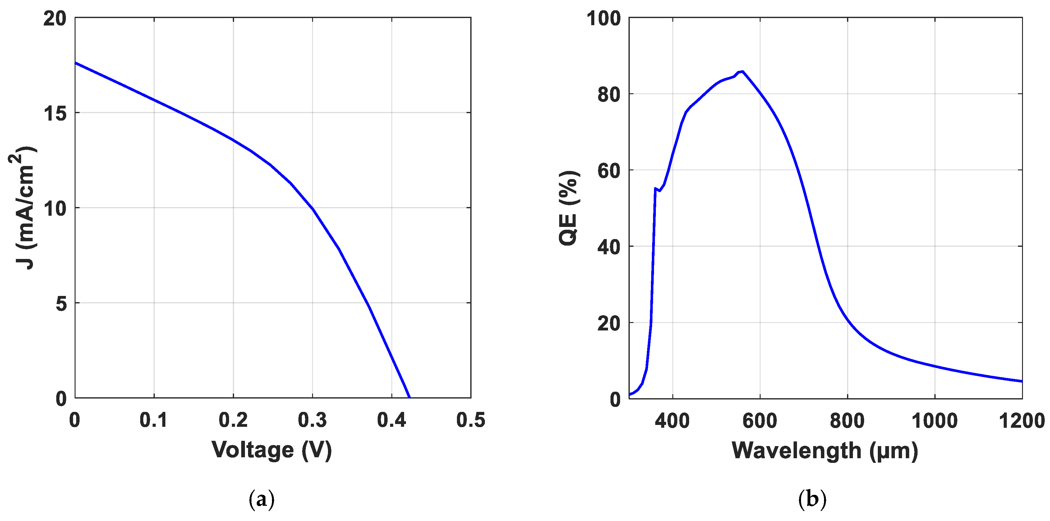
3.2.1. Structure and Calibration

To meet practical results, the simulation of the proposed PSC is started with the calibration of an experimental Cs2SnI6 PV device. Figure 9a illustrates the construction of the calibrated PV cell. The incident spectrum to the glass substrate is AM1.5G atmospheric mass spectrum. All investigated PSCs are simulated at room temperature. The FTO is exploited as a transparent conducting oxide (TCO). TiO2, and P3HT are the electron and hole transport materials, respectively. The simulation factors of the materials used are displayed in Table 4, while Table 5 lists the defect interface parameters. The JV characteristic curves of the experimental work and the calibration are illustrated in Figure 9b. As depicted in the figure, the JV characteristics of the calibrated cell exhibit a linear trend, suggesting potential issues with factors like series resistance (Rs), shunt resistance (Rsh), and bulk defects. Series resistance arises from the resistance encountered by the current flow through various components of the cell, including semiconductor material and contacts. In our calibrated cell, the computed series resistance is relatively high, approximately 6 Ω. Similarly, shunt resistance, representing resistance across the cell’s junction or bulk material, is low in our calibrated cell at around 50 Ω, allowing for unwanted leakage currents. Additionally, bulk defects within the semiconductor material create recombination centers, diverting charge carriers from contributing to the photocurrent. Adjusting the bulk defects to fit experimental data yielded a high defect density of approximately 1.68 × 1017 cm−3 (see Table 4), indicative of increased recombination losses and efficiency reduction. The output performance metrics of both the experimental and simulation cells, featuring stacked layers FTO/TiO2/Cs2SnI6/P3HT/Ag, are presented in Table 6 for comparison. As can be observed from Table 6, the simulation results align with the experimental findings.

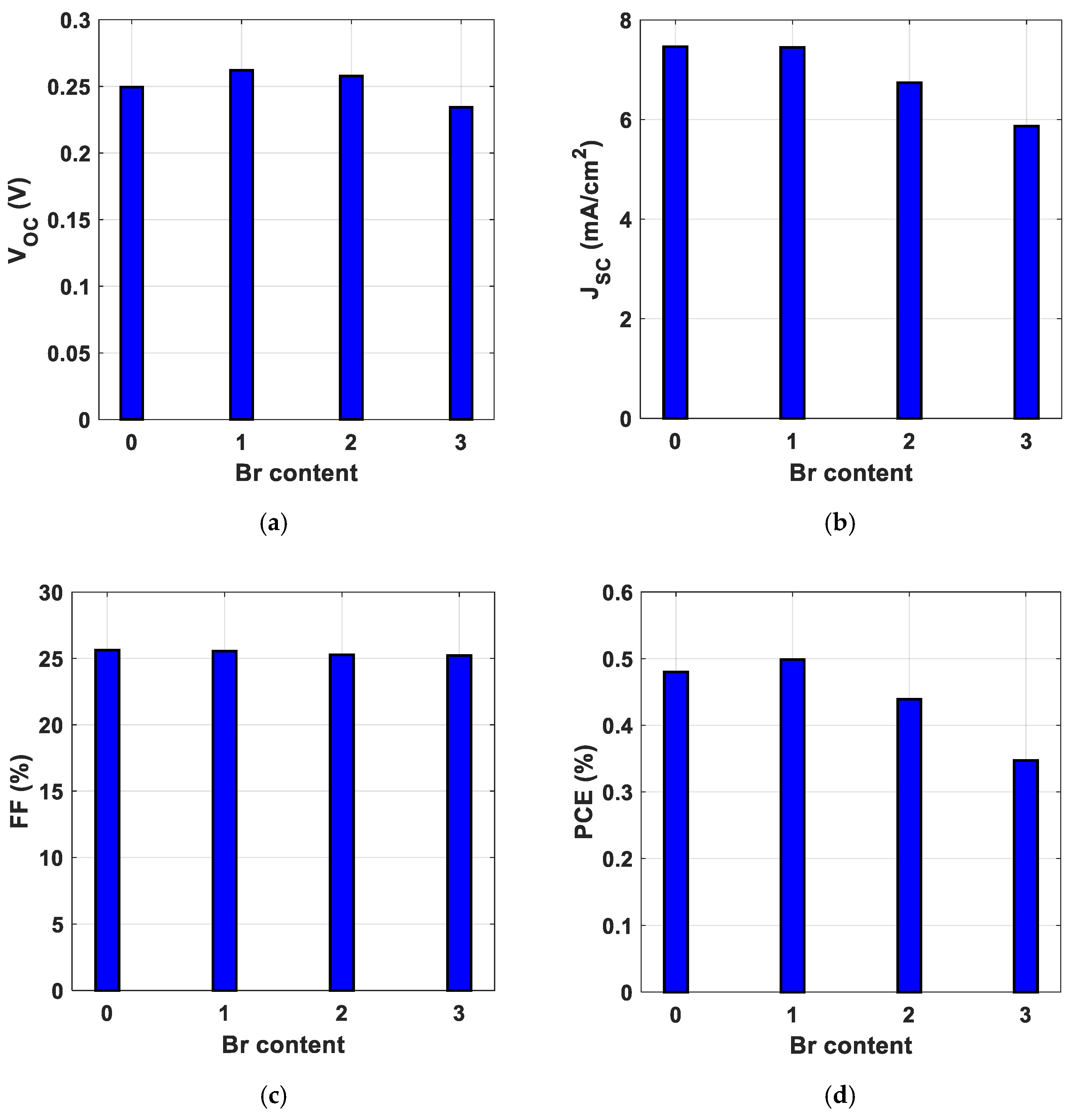
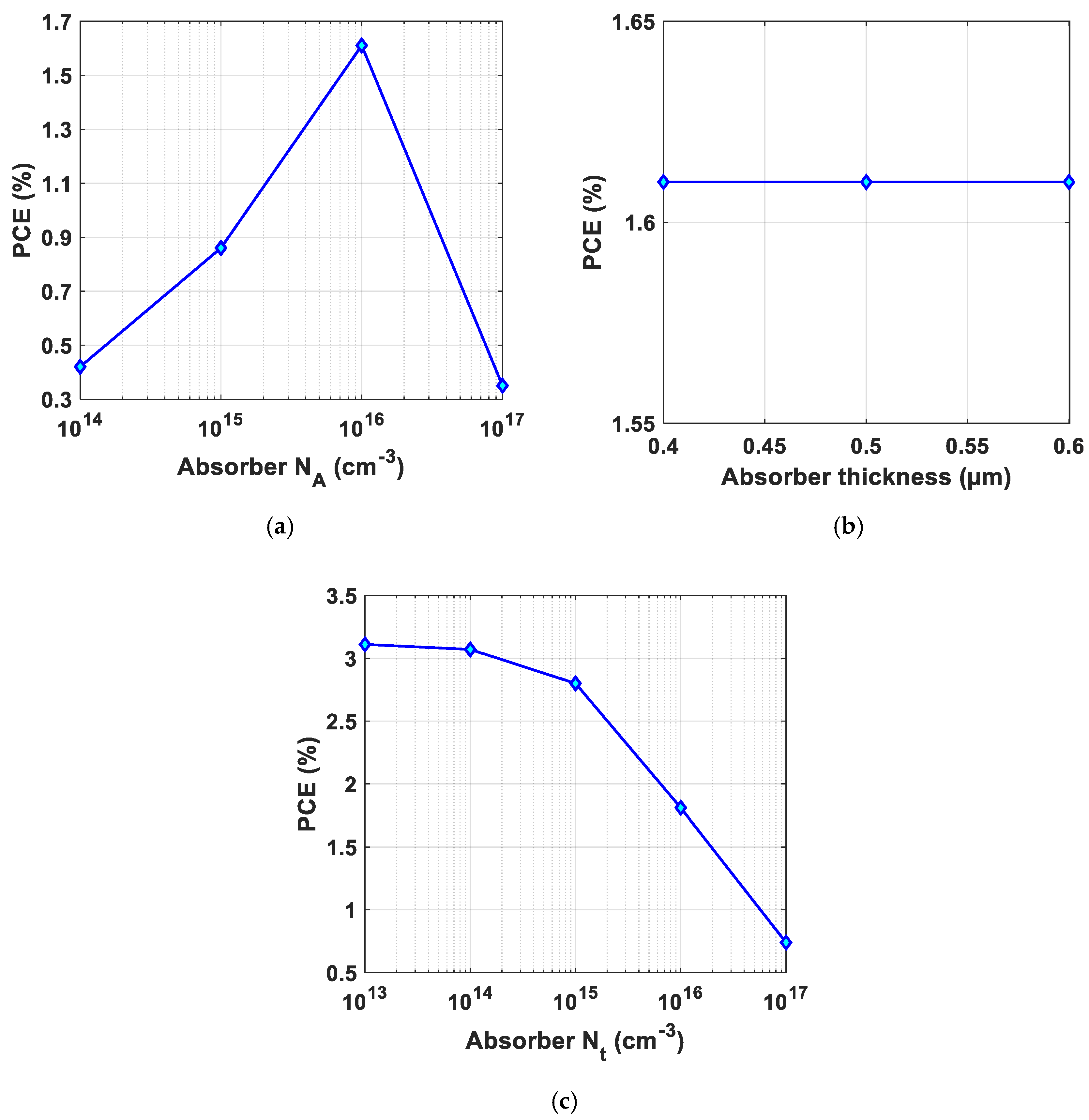
3.2.2. Solar Cell Optimization

In this Section, optimization of the perovskite absorber is performed to find possible routes to enhance its performance. Keeping the same ETL and HTL of the calibrated cell, Cs2SnI6 is replaced by Cs2SnI6−xBrx when Br atoms are substituted in the I site. The main material factors of three cases of Cs2SnI6−xBrx alloys (Cs2SnI5Br (x = 1), Cs2SnI4Br2 (x = 2), and Cs2SnI3Br3 (x = 3)) are recorded in Table 7. It should be noted here that we limit our analysis to values of Eg less than 2 eV, as according to the Shockley–Queisser limit the most suitable Eg is around 1.34 eV [65]. The output performance parameters with different Br contents are displayed in Figure 10. The case of Cs2SnI6 (x = 0) is also included for comparison. A maximum PCE of 0.5% is attained when Cs2SnI5Br is used as an absorber material, for which Eg = 1.339 eV.
Now, the doping density and the thickness of the photoactive layer of the structure of FTO/Cs2SnIBr5/Cs2SnI6/P3HT/Ag are optimized. Because it has the narrowest Eg, the Cs2SnI6 compound is selected as an absorber layer which allows it to absorb more of the spectrum with a higher cut-off wavelength. The doping of the absorber layer is investigated and an n-p-p+ structure is proposed. The highest PCE is 1.61% when the NA of the absorber layer is 1016 cm−3, as demonstrated in Figure 11a. The thickness of the photoactive layer is studied and has no effect on the PCE in the practical range of the perovskite film, as displayed in Figure 11b.
Moreover, the influence of the defect concentration of the absorber film on cell performance is examined. The defect concentration of the absorber has a profound effect on the PCE, as illustrated in Figure 11c. A defect density of 1014 cm−3 is selected to meet the practical range with a PCE of 3.07%, FF of 41.27%, JSC of 17.61 mA/cm2, and VOC of 0.42 V. Finally, the JV and QE of the optimized cell are illustrated in Figure 12a and 12b, respectively. Notably, the results indicate that the most crucial parameter that limits the cell performance is the trap concentration of the absorber.

4. Conclusions

In conclusion, employing the DFT method to analyze the structural, electronic, and optical properties of the Cs2SnI6−xBrx solid solution revealed that substituting Br with I led to an increase in the bandgap values from 1.33 to 2.24 eV. This trend is attributed to the difference in the atomic numbers between I and Br (ZI > ZBr), where a higher atomic number corresponds to a wider atomic potential. Furthermore, based on the free electron theory, as the overlap of atomic potentials increases or decreases, the Fourier coefficient for the periodic potential decreases or increases, leading to smaller or larger bandgap values, respectively. The calculated optical properties suggest that Cs2SnI6−xBrx alloys hold promise for various optoelectronic applications. Furthermore, evaluating the solar cell performance of Cs2SnI6−xBrx alloys demonstrated that the FTO/Cs2SnIBr5/Cs2SnI6/P3HT/Ag PSC structure achieved a PCE of 0.77%. Through optimization of the doping and thickness of the HTL, the PCE increased to 0.86%. Introducing a structure of n-p-p+ resulted in a PCE of 1.61%, while further optimization of the absorber film’s thickness and defect concentration yielded a PCE of 3.07%. Certainly, there are opportunities for improvement or further development, such as optimizing the interface engineering between the layers to minimize losses, exploring novel materials for more efficient charge transport, and refining the fabrication processes to reduce defects, which would make these solar cells more viable for practical applications.

Supplementary Materials

The following supporting information can be downloaded at https://www.mdpi.com/article/10.3390/physics7010003/s1, Figure S1: Flowchart of the methodology of solution in SCAPS–1D; Table S1: Physical quantities definitions in SCAPS–1D.

Author Contributions

All authors are contributed equally to this work. All authors have read and agreed to the published version of the manuscript.

Funding

The authors extend their appreciation to the Researchers Supporting Project number (RSP2025R394), King Saud University, Riyadh, Saudi Arabia.

Data Availability Statement

Data will be provided upon reasonable request from the corresponding author.

Conflicts of Interest

The authors declare no conflict of interest.

Abbreviations

AM1.5G Atmospheric Mass 1.5 Global (solar spectrum)
CB conduction band
CF capacitance–frequency
CV capacitance–voltage
DFT density functional theory
ETL electron transport layer
Expt. Experiment
FP–LAPW full potential linearized augmented plane wave
FTO fluoride-doped tin oxide
FFfill factor
GGA–WC Wu–Cohen generalized gradients approximation
HTL hole transport layer
IB intermediate band
IBZ irreducible Brillouin zone
JV current density-voltage
MT muffinn-tin
mBJ modified Becke–Johnson
OC open circuit
PCE power conversion efficiency
PSC perovskite solar cell
PV photovoltaic
QE quantum efficiency
SC solar cell
SCAPS solar cell capacitance simulator
TB–mBJ Tran and Blaha modified Becke–Johnson
TCOtransparent conducting oxide
UV ultraviolet
VB valence band
WD Wemple–DiDomenico
1D one-dimensional

References

  1. Shaheen, M.A.M.; Hasanien, H.M.; Turky, R.A.; Ćalasan, M.; Zobaa, A.F.; Aleem, S.H.E.A. OPF of modern power systems comprising renewable energy sources using improved chgs optimization algorithm. Energies 2021, 14, 6962. [Google Scholar] [CrossRef]
  2. Kojima, A.; Teshima, K.; Shirai, Y.; Miyasaka, T. Organometal halide perovskites as visible-light sensitizers for photovoltaic cells. J. Am. Chem. Soc. 2009, 131, 6050–6051. [Google Scholar] [CrossRef]
  3. Chung, I.; Song, J.-H.; Im, J.; Androulakis, J.; Malliakas, C.D.; Li, H.; Freeman, A.J.; Kenney, J.T.; Kanatzidis, M.G. CsSnI3: Semiconductor or metal? High electrical conductivity and strong near-infrared photoluminescence from a single material. high hole mobility and phase-transitions. ChemInform, 2012; 43, in print. [Google Scholar] [CrossRef]
  4. Gao, P.; Grätzel, M.; Nazeeruddin, M.K. Organohalide lead perovskites for photovoltaic applications. Energy Environ. Sci. 2014, 7, 2448–2463. [Google Scholar] [CrossRef]
  5. Colella, S.; Mosconi, E.; Fedeli, P.; Listorti, A.; Rizzo, A.; Gazza, F.; Orlandi, F.; Ferro, P.; Besagni, T.; Calestani, G.; et al. MAPbI3−xClx mixed halide perovskite for hybrid solar cells: The role of chloride as dopant on the transport and structural properties. MRS Proc. 2014, 1667, mrss14-1667-b03-02. [Google Scholar] [CrossRef]
  6. Eperon, G.E.; Paterno, G.M.; Sutton, R.J.; Zampetti, A.; Haghighirad, A.A.; Cacialli, F.; Snaith, H.J. Inorganic caesium lead iodide perovskite solar cells. J. Mater. Chem. A 2015, 3, 19688–19695. [Google Scholar] [CrossRef]
  7. NREL Photovaltic Research. Best Research-Cell Efficiency Chart. Available online: https://www.nrel.gov/pv/cell-efficiency.html (accessed on 25 November 2024).
  8. Liu, G.; Kong, L.; Gong, J.; Yang, W.; Mao, H.; Hu, Q.; Liu, Z.; Schaller, R.D.; Zhang, D.; Xu, T. Pressure-induced bandgap optimization in lead-based perovskites with prolonged carrier lifetime and ambient retainability. Adv. Funct. Mater. 2016, 27, 1604208. [Google Scholar] [CrossRef]
  9. Liu, H.; Siron, M.; Gao, M.; Lu, D.; Bekenstein, Y.; Zhang, D.; Dou, L.; Alivisatos, A.P.; Yang, P. Lead halide perovskite nanowires stabilized by block copolymers for Langmuir-Blodgett assembly. Nano Res. 2020, 13, 1453–1458. [Google Scholar] [CrossRef]
  10. Faheem, M.B.; Khan, B.; Feng, C.; Farooq, M.U.; Raziq, F.; Xiao, Y.; Li, Y. All-inorganic perovskite solar cells: Energetics, key challenges, and strategies toward commercialization. ACS Energy Lett. 2019, 5, 290–320. [Google Scholar] [CrossRef]
  11. Ju, M.-G.; Chen, M.; Zhou, Y.; Dai, J.; Ma, L.; Padture, N.P.; Zeng, X.C. Toward eco-friendly and stable perovskite materials for photovoltaics. Joule 2018, 2, 1231–1241. [Google Scholar] [CrossRef]
  12. Park, Y.; Jana, A.; Myung, C.W.; Yoon, T.; Lee, G.; Kocher, C.C.; Ying, G.; Osokin, V.; Taylor, R.A.; Kim, K.S. Enhanced photoluminescence quantum yield of MAPbBr3 nanocrystals by passivation using graphene. Nano Res. 2020, 13, 932–938. [Google Scholar] [CrossRef]
  13. Kaltzoglou, A.; Antoniadou, M.; Kontos, A.G.; Stoumpos, C.C.; Perganti, D.; Siranidi, E.; Raptis, V.; Trohidou, K.N.; Psycharis, V.; Kanatzidis, M.G.; et al. Optical-vibrational properties of the Cs2SnX6 (X = Cl, Br, I) defect perovskites and hole-transport efficiency in dye-sensitized solar cells. J. Phys. Chem. C 2016, 120, 11777–11785. [Google Scholar] [CrossRef]
  14. Wang, N.; Zhou, Y.; Ju, M.; Garces, H.F.; Ding, T.; Pang, S.; Zeng, X.C.; Padture, N.P.; Sun, X.W. Heterojunction-depleted lead-free perovskite solar cells with coarse-grained B-γ-CsSnI3 thin films. Adv. Energy Mater. 2016, 6, 1601130. [Google Scholar] [CrossRef]
  15. Hao, F.; Stoumpos, C.C.; Cao, D.H.; Chang, R.P.H.; Kanatzidis, M.G. Lead-free solid-state organic–inorganic halide perovskite solar cells. Nat. Photonics 2014, 8, 489–494. [Google Scholar] [CrossRef]
  16. Mastryukov, M.V.; Son, A.G.; Tekshina, E.V.; Vaimugin, L.A.; Kozyukhin, S.A.; Egorysheva, A.V.; Brekhovskikh, M.N. Effect of the purity of the precursor SnI2 on the optical properties of CsSnI3 perovskite thin films. Russ. J. Inorg. Chem. 2022, 67, 1652–1657. [Google Scholar] [CrossRef]
  17. Ran, C.; Gao, W.; Li, J.; Xi, J.; Li, L.; Dai, J.; Yang, Y.; Gao, X.; Dong, H.; Jiao, B.; et al. Conjugated organic cations enable efficient self-healing FASnI3 solar cells. Joule 2019, 3, 3072–3087. [Google Scholar] [CrossRef]
  18. Maughan, A.E.; Ganose, A.M.; Bordelon, M.M.; Miller, E.M.; Scanlon, D.O.; Neilson, J.R. Defect tolerance to intolerance in the vacancy-ordered double perovskite semiconductors Cs2SnI6 and Cs2TeI6. J. Am. Chem. Soc. 2016, 138, 8453–8464. [Google Scholar] [CrossRef] [PubMed]
  19. Combs, V.E.; Oswald, I.W.H.; Neilson, J.R. Hydrothermal crystal growth of mixed valence Cs2SbBr6. Cryst. Growth Des. 2019, 19, 4090–4094. [Google Scholar] [CrossRef]
  20. Ganesan, R.; Vinodhini, S.P.; Balasubramani, V.; Parthipan, G.; Sridhar, T.M.; Arulmozhi, R.; Muralidharan, R. Tuning the band gap of hybrid lead free defect perovskite nano crystals for solar cell applications. New J. Chem. 2019, 43, 15258–15266. [Google Scholar] [CrossRef]
  21. Liu, Y.; Gao, W.; Ran, C.; Dong, H.; Sun, N.; Ran, X.; Xia, Y.; Song, L.; Chen, Y.; Huang, W. All-inorganic Sn-based perovskite solar cells: Status, challenges, and perspectives. ChemSusChem 2020, 13, 6477–6497. [Google Scholar] [CrossRef]
  22. Rahim, W.; Cheng, A.; Lyu, C.; Shi, T.; Wang, Z.; Scanlon, D.O.; Palgrave, R.G. Geometric analysis and formability of the cubic A2BX6 vacancy-ordered double perovskite structure. Chem. Mater. 2020, 32, 9573–9583. [Google Scholar] [CrossRef]
  23. Faizan, M.; Khan, S.H.; Khachai, H.; Seddik, T.; Bin Omran, S.; Khenata, R.; Xie, J.; Al-Anazy, M.M. Electronic, optical, and thermoelectric properties of perovskite variants A2BX 6: Insight and design via first-principles calculations. Int. J. Energy Res. 2020, 45, 4495–4507. [Google Scholar] [CrossRef]
  24. Euvrard, J.; Wang, X.; Li, T.; Yan, Y.; Mitzi, D.B. Is Cs2TiBr6 a promising Pb-free perovskite for solar energy applications? J. Mater. Chem. A 2020, 8, 4049–4054. [Google Scholar] [CrossRef]
  25. Jong, U.-G.; Yu, C.-J.; Kye, Y.-H. Computational prediction of structural, electronic, and optical properties and phase stability of double perovskites K2SnX6 (X = I, Br, Cl). RSC Adv. 2019, 10, 201–209. [Google Scholar] [CrossRef]
  26. Bousahla, M.A.; Faizan, M.; Seddik, T.; Bin Omran, S.; Khachai, H.; Laref, A.; Khenata, R.; Znaidia, S.; Boukhris, I.; Khan, S.H. DFT study on the crystal structure, optoelectronic, and thermoelectric properties of lead-free inorganic A2PdBr6 (A = K, Rb, and Cs) perovskites. Mater. Today Commun. 2021, 30, 103061. [Google Scholar] [CrossRef]
  27. Cheghib, N.; Maizi, R.; Boudjahem, A.-G.; Ksouri, R.; Derdare, M. Theoretical study of the elastic, electronic, and thermodynamic properties of the Cs2MF6 (M = Cr and Mo) perovskites. Russ. J. Inorg. Chem. 2024; in print. [Google Scholar] [CrossRef]
  28. Ksouri, R.; Maizi, R.; Boudjahem, A.-G.; Cheghib, N.; Djaghout, I.; Derdare, M. DFT Study of structural, elastic, electronic, and thermodynamic properties of compounds Cs2TiCl6 and Cs2TiBr6. Russ. J. Inorg. Chem. 2024; in print. [Google Scholar] [CrossRef]
  29. Saparov, B.; Sun, J.-P.; Meng, W.; Xiao, Z.; Duan, H.-S.; Gunawan, O.; Shin, D.; Hill, I.G.; Yan, Y.; Mitzi, D.B. Thin-film deposition and characterization of a Sn-deficient perovskite derivative Cs2SnI6. Chem. Mater. 2016, 28, 2315–2322. [Google Scholar] [CrossRef]
  30. Barker, A.J.; Sadhanala, A.; Deschler, F.; Gandini, M.; Senanayak, S.P.; Pearce, P.M.; Mosconi, E.; Pearson, A.J.; Wu, Y.; Kandada, A.R.S.; et al. Defect-assisted photoinduced halide segregation in mixed-halide perovskite thin films. ACS Energy Lett. 2017, 2, 1416–1424. [Google Scholar] [CrossRef]
  31. Rezini, B.; Seddik, T.; Mouacher, R.; Vu, T.V.; Batouche, M.; Khyzhun, O.Y. Strain effects on electronic, optical properties and carriers mobility of Cs2SnI6 vacancy-ordered double perovskite: A promising photovoltaic material. Int. J. Quant. Chem. 2022, 122, e26977. [Google Scholar] [CrossRef]
  32. Yuan, G.; Huang, S.; Niu, J.; Qin, S.; Wu, X.; Ding, H.; Lu, A. Compressibility of Cs2SnBr6 by X-ray diffraction and Raman spectroscopy. Solid State Commun. 2018, 275, 68–72. [Google Scholar] [CrossRef]
  33. Tan, Z.; Li, J.; Zhang, C.; Li, Z.; Hu, Q.; Xiao, Z.; Kamiya, T.; Hosono, H.; Niu, G.; Lifshitz, E.; et al. Highly efficient blue-emitting bi-doped Cs2SnCl6 perovskite variant: Photoluminescence induced by impurity doping. Adv. Funct. Mater. 2018, 28, 1801131. [Google Scholar] [CrossRef]
  34. Qiu, X.; Cao, B.; Yuan, S.; Chen, X.; Qiu, Z.; Jiang, Y.; Ye, Q.; Wang, H.; Zeng, H.; Liu, J.; et al. From unstable CsSnI3 to air-stable Cs2SnI6: A lead-free perovskite solar cell light absorber with bandgap of 1.48 eV and high absorption coefficient. Sol. Energy Mater. Sol. Cells 2017, 159, 227–234. [Google Scholar] [CrossRef]
  35. Lee, B.; Stoumpos, C.C.; Zhou, N.; Hao, F.; Malliakas, C.; Yeh, C.-Y.; Marks, T.J.; Kanatzidis, M.G.; Chang, R.P.H. Air-stable molecular semiconducting iodosalts for solar cell applications: Cs2SnI6 as a hole conductor. J. Am. Chem. Soc. 2014, 136, 15379–15385. [Google Scholar] [CrossRef]
  36. Kapil, G.; Ohta, T.; Koyanagi, T.; Vigneshwaran, M.; Zhang, Y.; Ogomi, Y.; Pandey, S.S.; Yoshino, K.; Shen, Q.; Toyoda, T.; et al. Investigation of interfacial charge transfer in solution processed Cs2SnI6 thin films. J. Phys. Chem. C 2017, 121, 13092–13100. [Google Scholar] [CrossRef]
  37. Jung, H.S.; Park, N. Perovskite solar cells: From materials to devices. Small 2014, 11, 10–25. [Google Scholar] [CrossRef] [PubMed]
  38. Lee, B.; Krenselewski, A.; Baik, S.I.; Seidman, D.N.; Chang, R.P.H. Solution processing of air-stable molecular semiconducting iodosalts, Cs2SnI6−xBrx, for potential solar cell applications. Sustain. Energy Fuels 2017, 1, 710–724. [Google Scholar] [CrossRef]
  39. Yuan, G.; Huang, S.; Qin, S.; Wu, X.; Ding, H.; Lu, A. Structural, optical, and thermal properties of Cs2SnI6–xBrx mixed perovskite solid solutions. Eur. J. Inorg. Chem. 2019, 2019, 2524–2529. [Google Scholar] [CrossRef]
  40. Han, X.; Liang, J.; Yang, J.; Soni, K.; Fang, Q.; Wang, W.; Zhang, J.; Jia, S.; Martí, A.A.; Zhao, Y.; et al. Lead-free double perovskite Cs2SnX6: Facile solution synthesis and excellent stability. Small 2019, 15, 1901650. [Google Scholar] [CrossRef] [PubMed]
  41. Qamar, S.; Sultan, M.; Akhter, Z.; Ela, S.E. A facile one-step solution synthesis of Cs2SnI6−xBrx using less-toxic methanol solvent for application in dye-sensitized solar cells. Int. J. Energy Res. 2022, 46, 13441–13452. [Google Scholar] [CrossRef]
  42. Nazir, S.; Noor, N.; Khan, M.A.; Mumtaz, S.; Elansary, H.O. DFT study of optoelectronic and thermoelectric properties of pure and doped double perovskite Cs2SnI6 for solar cell applications. Chem. Phys. Lett. 2024, 852, 141519. [Google Scholar] [CrossRef]
  43. Zhang, J.; Yang, C.; Liao, Y.; Li, S.; Yang, P.; Xi, Y.; Cai, C.; Liu, W. Investigating optical adsorption properties of lead-free double perovskite semiconductors Cs2SnI6−xBrx (x = 0–6) via first principles calculation. Microw. Opt. Technol. Lett. 2021, 65, 1017–1023. [Google Scholar] [CrossRef]
  44. Guo, S.; Zhang, Q.; Sa, R.; Liu, D. Exploring the stability and physical properties of double perovskite Cs2SnI6 by doping the Cl/Br atom: A DFT study. Comput. Theor. Chem. 2022, 1209, 113609. [Google Scholar] [CrossRef]
  45. Madsen, G.K.H.; Blaha, P.; Schwarz, K.; Sjöstedt, E.; Nordström, L. Efficient linearization of the augmented plane-wave method. Phys. Rev. B 2001, 64, 195134. [Google Scholar] [CrossRef]
  46. Blaha, P.; Schwarz, K.; Madsen, G.; Kvasnicka, D.; Luitz, J. WIEN2k: An Augmented Plane Wave Plus Local Orbitals Program for Calculating Crystal Properties. User’s Guide, WIEN2k 14.2; Vienna University of Technology, Institute of Physical and Theoretical Chemistry: Vienna, Austria, 2014; Available online: https://indico.cells.es/event/53/attachments/541/841/WIEN2k_usersguide.pdf (accessed on 25 November 2024).
  47. Tran, F.; Blaha, P. Accurate band gaps of semiconductors and insulators with a semilocal exchange-correlation potential. Phys. Rev. Lett. 2009, 102, 226401. [Google Scholar] [CrossRef]
  48. Ketelaar, J.A.A.; Rietdijk, A.A.; van Staveren, C.H. Die Kristallstruktur von Ammonium-, Kalium-, Rubidium- und Cäsiumstannibromid. Recl. Trav. Chim. Pays-Bas 1937, 56, 907–908. [Google Scholar] [CrossRef]
  49. Stoumpos, C.C.; Malliakas, C.D.; Kanatzidis, M.G. Semiconducting tin and lead iodide perovskites with organic cations: Phase transitions, high mobilities, and near-infrared photoluminescent properties. Inorg. Chem. 2013, 52, 9019–9038. [Google Scholar] [CrossRef]
  50. Wang, G.; Wang, D.; Shi, X. Electronic structure and optical properties of Cs2AX2′X4 (A = Ge, Sn, Pb; X′, X = Cl, Br, I). AIP Adv. 2015, 5, 127224. [Google Scholar] [CrossRef]
  51. Yang, X.; Wang, Y.; Jiang, J.; Li, M.; Tang, Z.; Cai, H.; Zhang, F.; Wu, X. Composition effects on structure and optical properties in double perovskite derivatives semiconductors Cs2SnI6−xBrx (x = 0–6). APL Mater. 2020, 8, 021102. [Google Scholar] [CrossRef]
  52. Green, M.A. Multiple band and impurity photovoltaic solar cells: General theory and comparison to tandem cells. Prog. Photovolt. Res. Appl. 2001, 9, 137–144. [Google Scholar] [CrossRef]
  53. Huang, H.-M.; Jiang, Z.-Y.; Luo, S.-J. First-principles investigations on the mechanical, thermal, electronic, and optical properties of the defect perovskites Cs2SnX6 (X = Cl, Br, I). Chin. Phys. B 2017, 26, 096301. [Google Scholar] [CrossRef]
  54. Rasukkannu, M.; Velauthapillai, D.; Vajeeston, P. A first-principle study of the electronic, mechanical and optical properties of inorganic perovskite Cs2SnI6 for intermediate-band solar cells. Mater. Lett. 2018, 218, 233–236. [Google Scholar] [CrossRef]
  55. Cai, Y.; Xie, W.; Ding, H.; Chen, Y.; Thirumal, K.; Wong, L.H.; Mathews, N.; Mhaisalkar, S.G.; Sherburne, M.; Asta, M. Computational study of halide perovskite-derived A2BX6 inorganic compounds: Chemical trends in electronic structure and structural stability. Chem. Mater. 2017, 29, 7740–7749. [Google Scholar] [CrossRef]
  56. Ouerghui, W.; Alkhalifah, M.S. Density functional investigation of structural, electronic, optical and thermodynamic properties of Zn1−xBexO semiconductor. Appl. Phys. A 2019, 125, 374. [Google Scholar] [CrossRef]
  57. Ben Abdallah, H.; Ouerghui, W. Hybrid functional calculations of electro-optical properties of novel Ga1−xInxTe ternary chalcogenides. Appl. Phys. A 2020, 126, 1–12. [Google Scholar] [CrossRef]
  58. Ouerghui, W.; Alkhalifah, M.S.; Ben Abdallah, H. DFT calculations on ZnO1−x compounds for optoelectronic applications. J. Comput. Electron. 2021, 20, 467–479. [Google Scholar] [CrossRef]
  59. Ben Abdallah, H.; Ouerghui, W. Spin–orbit coupling effect on electronic, linear and nonlinear optical properties of Bi2S3 and the ternary bismuth sulfide Bi2S2.75Se0.25: Ab-initio calculations. Opt. Quant. Electron. 2021, 54, 20. [Google Scholar] [CrossRef]
  60. Ouerghui, W.; Gassoumi, M.; Beji, L.; Maaref, M. Optical properties of quaternary GaMnAsP thin layer grown by molecular beam epitaxy. Physica E Low-dim.l Syst. Nanostr. 2021, 131, 114733. [Google Scholar] [CrossRef]
  61. Basyoni, M.S.S.; Salah, M.M.; Mousa, M.; Shaker, A.; Zekry, A.; Abouelatta, M.; Alshammari, M.T.; Al-Dhlan, K.A.; Gontrand, C. On the investigation of interface defects of solar cells: Lead-based vs lead-free perovskite. IEEE Access 2021, 9, 130221–130232. [Google Scholar] [CrossRef]
  62. Srivastava, P.; Sadanand, S.; Rai, S.; Lohia, P.; Dwivedi, D.K.; Qasem, H.; Umar, A.; Akbar, S.; Algadi, H.; Baskoutas, S. Theoretical study of perovskite solar cell for enhancement of device performance using SCAPS-1D. Phys. Scr. 2022, 97, 125004. [Google Scholar] [CrossRef]
  63. Salem, M.S.; Shaker, A.; Almurayziq, T.S.; Alshammari, M.T. Prospective efficiency boosting of full-inorganic single-junction Sb2(S, Se)3 solar cell. Sol. Energy Mater. Sol. Cells 2022, 248, 112001. [Google Scholar] [CrossRef]
  64. Jiang, Y.; Zhang, H.; Qiu, X.; Cao, B. The air and thermal stabilities of lead-free perovskite variant Cs2SnI6 powder. Mater. Lett. 2017, 199, 50–52. [Google Scholar] [CrossRef]
  65. Shockley, W.; Queisser, H.J. Detailed balance limit of efficiency of p-n junction solar cells. J. Appl. Phys. 1961, 32, 510–519. [Google Scholar] [CrossRef]
Figure 1. Organizational workflow for optimizing Cs2SnI6−xBrx perovskite solar cell performance using DFT and SCAPS–1D.
Physics 07 00003 g001
Figure 2. The crystal structure of Cs2SnI6−xBrx for x = 0, 1, 2, 3, 4, 5, and 6.
Physics 07 00003 g002
Figure 3. Electronic band structures and the densities of states of (a) Cs2SnI6 and (b) Cs2SnBr6. See text for details.
Physics 07 00003 g003aPhysics 07 00003 g003b
Figure 4. Electronic band structures and the densities of states of Cs2SnI6−xBrx alloys for x = 1, 2, 3, 4, and 5. Notations as in Figure 3.
Physics 07 00003 g004aPhysics 07 00003 g004b
Figure 5. Energy band gaps of Cs2SnI6−xBrx alloys versus Br content, x. The plotted data compare our DFT calculation and measurements from Ref. [39].
Physics 07 00003 g005
Figure 6. Photon-energy dependence of the calculated linear optical constants of Cs2SnI6−xBrx alloys: real (a) and imaginary (b) parts of the dielectric function, refractive index (c), and reflectivity (d).
Physics 07 00003 g006
Figure 7. Calculated absorption coefficient of Cs2SnI6−xBrx alloys.
Physics 07 00003 g007
Figure 8. ( n 2 1 ) 1   versus ( h ν ) 2 (see Equation (4)) for Cs2SnI6−xBrx alloys.
Physics 07 00003 g008
Figure 9. Calibration of PSC: (a) main structure and (b) JV characteristic curves representing both simulation and experimental data. See text for details.
Physics 07 00003 g009
Figure 10. The output performance parameters of the PSC with different Br contents (a) VOC, (b) JSC, (c) FF, and (d) PCE.
Physics 07 00003 g010
Figure 11. The dependance of the PCE on (a) absorber doping, (b) absorber thickness, and (c) absorber defect density.
Physics 07 00003 g011
Figure 12. The performance characteristics of the optimized cells: (a) JV and (b) QE curves.
Physics 07 00003 g012
Table 1. Calculated lattice parameters of the current study compared with those in literature.
AlloysCs2SnI6Cs2SnI5Br1Cs2SnI4Br2Cs2SnI3Br3Cs2SnI2Br4Cs2SnI1Br5Cs2SnBr6
This study 11.59011.46211.32211.18711.02910.86910.837
Expt.11.638 a11.528 e11.41 e11.274 e11.147 e10.961 e10.837 a
11.652 b------
11.627 c-----10.77 b
11.646 e-----10.859 e
11.67 f-----10.83 f
Theory12.016 a-----11.218 a
12.032 d-----11.243 d
a [34], b [48], c [49], d [50], e [38], f [51]. “Expt.” stands for experimental results.
Table 2. Computed band gap Eg (in eV) and hole and electron effective masses (mh* and me*) of Cs2SnI6−xBrx alloys compared with other experimental and theoretical values.
AlloysEgme*mh*
PresentExpt.TheoryPresentExpt.TheoryPresentExpt.Theory
Cs2SnI61.2571.26 a, 1.24 c, 1.3 d, 1.25 e1.28 c, 0.36 f, 0.92 f, 0.883 b0.272 0.152 g,
0.306 g, 0.33 h
1.851 1.4173 g
1.852 g, 1.5 h
Cs2SnI5Br11.331.34 e, 1.32 c, 1.375 d 0.281 1.692
Cs2SnI4Br21.421.43 e, 1.34 c,
1.4 d
0.285 0.967
Cs2SnI3Br31.521.53 e
1.46 c
1.68 c0.292 1.108
Cs2SnI2Br41.691.7 e, 1.5 c,
1.63 d
0.288 1.093
Cs2SnI1Br52.242.25 e, 1.75 c,
2.36 d
0.361 2.213
Cs2SnBr62.692.7 b, 2.93 c,
2.85 d, 3.01 e
2.9 c, 1.51 f, 2.36 f, 2.241 b0.39 2.574
a [35], b [13], c [51], d [38], e [39], f [53], g [54], h [55].
Table 3. Calculated optical constants for Cs2SnI6−xbrx alloys: static dielectric constant ε1(0), static refractive index n(0), static reflectivity R(0), binding energy Eb, dispersion energy Ed, oscillator energy E0 and oscillator strength F .
Compound ε 1 0 n 0 R(0) (%) E b   ( m e V ) E d   ( e V ) E 0   ( e V ) F   ( e V 2 )
Cs2SnI63.861.9810.821613.514.6062.14
Cs2SnI5Br3.851.9610.622113.864.8066.52
Cs2SnI4Br23.841.9410.220314.065.0771.28
Cs2SnI3Br33.771.85922114.35.8283.22
Cs2SnI2Br43.701.828.4622615.216.5799.92
Cs2SnI1Br53.241.777.7740215.887.40117.51
Cs2SnBr63.151.777.8346416.227.50121.65
Table 4. Material parameters of the Cs2SnI6 PSCs.
FTO [61]TiO2 [61]Cs2SnI6P3HT [62]
d (thickness, nm)50030650100
Eg (bandgap, eV)3.53.21.2571.7
χ (electron affinity, eV)444.013.5
εr (Permittivity)997.23
Nc (effective DOS at CB, 1/cm3)2.2 × 10182 × 10183.569 × 10182 × 1018
Nv (effective DOS at VB, 1/cm3)1.8 × 10191.8 × 10191.21 × 10192 × 1019
µn (electron mobility, cm2/V s)202091.8 × 10−3
µp (hole mobility, cm2/V s)101091.8 × 10−2
ND (doping density n-type, 1/cm3)2 × 10191 × 1017 00
NA (doping density p-type, 1/cm3)0010151019
Nt (defect density, 1/cm3)101510151.68 × 10171015
σn (capture cross-section electrons, cm2)10−152 × 10−142 × 10−1410−15
σp (capture cross-section holes, cm2)10−152 × 10−142 × 10−14 10−15
Trap energy level (eV)0.60.60.60.8
Energetic distributionSingleGaussianGaussianGaussian
Table 5. Main factors of defects at interfaces [61,63].
HTL/Absorber Layer
or Absorber Layer/ETL
TypeNeutral
σn (cm2)10−15
σp (cm2)10−15
DistributionSingle
Energy level Et (eV)0.6
(above the highest Ev)
Total density (1/cm2)1016
Table 6. Comparison between quantitative simulation and experimental results.
VOC
(V)
JSC
(mA/cm2)
FF
(%)
PCE
(%)
Experiment [64]0.2567.4124.500.47
Simulation0.2497.4625.630.48
Table 7. Cs2SnI6−xBrx materials parameters.
Cs2SnI5BrCs2SnI4Br2Cs2SnI3Br3
Eg (eV)1.3391.4281.528
χ (eV)4.034.054.06
εr (permittivity)7.137.067.05
Nc (1/cm3)3.581 × 10183.652 × 10183.522 × 1018
Nv (1/cm3)4.8 × 10192.08 × 10192.19 × 1019
Disclaimer/Publisher’s Note: The statements, opinions and data contained in all publications are solely those of the individual author(s) and contributor(s) and not of MDPI and/or the editor(s). MDPI and/or the editor(s) disclaim responsibility for any injury to people or property resulting from any ideas, methods, instructions or products referred to in the content.

