Communication

Casimir Forces between a Dielectric and Metal: Compensation of the Electrostatic Interaction

by
Vitaly B. Svetovoy
Frumkin Institute of Physical Chemistry and Electrochemistry, Russian Academy of Sciences, Leninsky Prospect 31 bld. 4, 119071 Moscow, Russia
Physics 2023, 5(3), 814-822; https://doi.org/10.3390/physics5030051
Submission received: 15 June 2023 / Revised: 7 July 2023 / Accepted: 11 July 2023 / Published: 25 July 2023
(This article belongs to the Special Issue 75 Years of the Casimir Effect: Advances and Prospects)

Abstract

:
The Casimir forces between metals or good conductors have been checked experimentally. Semiconductors and especially dielectrics have not been investigated because of the surface charges, which generate strong electrostatic forces. Here, it is proposed to study the Casimir interaction of a dielectric and metal using a thin dielectric layer deposited on an optically thick metallic substrate. If the thickness of the layer is a few tens of nanometers, the electrostatic force due to charging can be compensated for by applying an extra voltage between the metallic plates. On the other hand, the contribution of the dielectric layer to the Casimir force is sufficiently large to extract information about the interaction between the bulk dielectric and metal.

1. Introduction

The Casimir forces [1] between bulk bodies have been intensely investigated during the last 20 years (see reviews [2,3,4,5]). Critical experiments have been performed in vacuum with a high precision at distances of the order of 100 nm [6,7,8,9]. A theoretical description of these forces generated by thermal and quantum fluctuations of the electromagnetic field has been proposed by Evgeniy Lifshitz and later developed along with his colleagues, Igor Dzyaloshinskii and Lev Pitaevskii [10,11]. Predictions of the Lifshitz theory have been checked in special experiments. The dependence of the Casimir forces on the dielectric functions of interacting materials has been verified [12,13,14,15,16,17], including magnetic materials [18,19]. Shorter distances up to 10 nm have been explored [20,21] and the importance of the effects of surface roughness has been stressed [22,23]. Larger distances in the range of micrometers have been carefully investigated experimentally [24,25,26,27] and it was found that there are some systematic deviations in the thermal contribution to the force.
The total force that is directly measured in the experiments includes the Casimir and electrostatic forces. The latter to be considered a background effect and has to be excluded. To minimize the electrostatic force, nearly all experiments have been performed with well-conducted materials but, even for good conductors, the electrostatic contribution to the total force is still important. The electrostatic force originates from the contact potential difference between different materials. However, even for similar interacting materials, the contact potential is nonzero because of the potential difference in the external circuit.
Dielectrics have never been used for force measurements because they contain trapped charges resulting in a strong electrostatic contribution. Even for semiconductors, only a few special cases have been tackled: silicon passivated with hydrogen (H-terminated) [13,28] that prevents oxidation and silicon carbide heavily doped with nitrogen [21], which behaves similar to metals. In general, the effect of charging significantly restricts the choice of materials that can be used for measurements of the Casimir forces.
Investigation of the insulating materials has been concentrated on the space charge in materials [29,30], where the trapped charges in localized states are produced by irradiation, ionization or injection. For thick dielectrics, the charging can be non-homogeneous in depth but, here, one considered homogeneously charged thin dielectric layers on metallic surfaces. The charging mechanisms in general are rather complicated but the total concentration of the surface charges can vary in the range of 10 10 10 13 cm 2 depending on the technological processing, with typical values in the range of 10 11 10 12 cm 2 .
The purpose of this paper is to demonstrate that the electrostatic force between two metals, one of which is covered by a thin dielectric layer, can be compensated for by applying an external potential between the bodies. Only for thick dielectrics is it not possible to compensate for the electrostatic force. It is also demonstrated that a layer with a thickness of a few tens of nanometers is sufficient to extract information about the Casimir interaction of the dielectric and metal. Only metallic substrates are considered here to concentrate on the main idea but not on the technical details. The application of the same idea applied to semiconductor substrates will be considered elsewhere. The problem solved in this paper is rather simple but, to the best of our knowledge, it has not been discussed in relation to the Casimir force measurements.

2. Electrostatic Interaction of Metals Covered by the Dielectric

Let us consider the electrostatic force between two metal plates, one of which is covered by a thin dielectric layer (see Figure 1). The dielectric can be deposited on the metal surface in a controlled way, for example, by magnetron sputtering. The dielectric layer with the thickness d can be made of any chemical compound and is charged with the bulk density ρ 0 . The Casimir force will be larger if only one metal is covered by the dielectric, so let us consider this configuration. In the experiments measuring the Casimir forces, researchers always try to avoid surface charges. When the force is measured between metals, the residual potential difference can be compensated for by applying an external voltage between the metals, as has been carried out in all the experiments [6,7,8,9]. If one metal has a dielectric covering, one has to take into account a finite concentration of charges in the dielectric. Here, we are going to answer the question: is it possible to compensate for the electrostatic force in this case?

2.1. Solution of the Electrostatic Problem

The structure under investigation is shown in Figure 1. The relative dielectric functions ε 1 , 2 and ε d are, in general, functions of frequency, ω , but, for the electrostatic interaction ( ω 0 ), ε d is a constant and ε 1 , 2 . Let the potential the metal 1 be Ψ 1 ; however, the potential of metal 2 can be chosen to be zero: Ψ 2 = 0 . In between the metals, the potential is described by the Poisson equation
d 2 Ψ d x 2 = 0 , 0 < x < h , ρ 0 / ε 0 ε d r m , h < x < h + d ,
where ε 0 is the permittivity of the vacuum.
The external boundary conditions are chosen as Ψ ( 0 ) = Ψ 1 and Ψ ( h + d ) = 0 . The solution that obeys the external boundary conditions is
Ψ ( x ) = Ψ 0 + A x , 0 < x < h , ρ 0 ( x h d ) 2 2 ε 0 ε d + B ( x h d ) , h < x < h + d ,
where A and B are unknown constants which are defined by the internal boundary conditions. At the vacuum–dielectric interface x = h , these are the continuity of the potential and electric displacement. Some surface charges can exist in the dielectric at the interface with the metal. However, in contrast with semiconductors, those charges do not contribute because the static dielectric constant of metals is going to infinity. Thus, the internal boundary conditions are
Ψ ( h δ ) = Ψ ( h + δ ) , d Ψ d x h δ = ε d d Ψ d x h + δ , δ 0 .
The electric field, E, in the vacuum gap is E = A and the electrostatic pressure between the plates is defined by the normal component of the Maxwell stress tensor, P e = ε 0 E 2 / 2 , (minus sign because the force is attractive). Determining the constant A from the internal boundary conditions, one finds, for the pressure:
P e = ε 0 2 ( ρ 0 d / ε 0 ) ( d / 2 ε d ) Ψ 1 h + d / ε d 2 .
If there are no trapped charges in the dielectric ( ρ 0 = 0 ), the only difference in the electrostatic pressure between metals is the effective increase in the distance between the plates, which is h eff = h + d / ε d . At a finite density of charges, the metal potential, Ψ 1 , is shifted to the value,
Δ U = ρ 0 d ε 0 d 2 ε d ,
where one can interpret ρ 0 d as the projection of the charge density on the surface.
In most of the Casimir force experiments, a sphere–plate configuration is used for measurements and the electrostatic force has to be defined for this configuration. The electrostatic force acting between the sphere and the plate can be immediately found from Equation (4) by applying the proximity force approximation (Derjaguin’s approximation [31,32]), which is true for h R , where R is the radius of the sphere. Then, one finds the electrostatic force between the sphere and the plate:
F e π R ε 0 2 ( ρ 0 d / ε 0 ) ( d / 2 ε d ) Ψ 1 2 h + d / ε d .
This result also depends on the shifted potential and effective distance. The exact expression for the force can be found analytically, but one can expect that this expression can also depend on the shifted potential and effective distance. It is worth noting that, at short distances, the roughness of the interacting surfaces starts to contribute. One can deal with the electrostatic forces on the same basis as was proposed for the Casimir forces [23].

2.2. Compensation of the Surface Charges

In all the experiments, both plates (more often it is a sphere and plate) are grounded. Nevertheless, Ψ 1 is nonzero and can be as large as 100 mV or so. This value is due to the contact potential difference, V c : Ψ 1 = V c . In the case of two metals, this potential can be compensated for by applying the external voltage between the bodies as equal to V c . Equation (4) shows that one can also compensate for the electrostatic force between two metals, one of which is covered by the dielectric. If the external voltage is U, then Ψ 1 = V c + U and one finds the compensating potential,
U = V c + Δ U .
Thus, in the case of the charged dielectric, one has to apply, in addition to V c , an extra voltage, Δ U , which is proportional to the density of charges in the dielectric. Similarly to the two metals case, the compensating potential does not depend on the distance, h, between the plates.
Consider an example where metal 2 is covered by silicon dioxide with the dielectric constant, ε d = 3.9 . It is convenient to consider as a parameter the surface charge density
σ s = ρ 0 d 0 , d 0 = 10 nm .
The expected value for this parameter [30] is in the range of | σ s | = 10 8 10 7 C/cm 2 (concentration of the surface charges N s 10 11 10 12 cm 2 ). The extra voltage needed to compensate for the electrostatic force is estimated to be in the range of
| Δ U | = ( 14.5 145 ) ( d / d 0 ) 2 mV .
If one considers | Δ U | < 1 V as a realistic compensating potential, then Equation (9) restricts the thickness of the dielectric layer. From this restriction, one can conclude that, for the largest charge density, the dielectric film thickness has to be smaller than 26 nm and, for the smallest | σ s | = 10 8 C/cm 2 , it has to be smaller than 83 nm. Now, the question is: can one obtain information about the Casimir interaction between the metal and dielectric measuring the force between two metals, one of which is covered by the dielectric with a thickness of approximately 40 nm?

3. Casimir Interaction of Metal Covered by the Dielectric

Let us consider the Casimir force in the configuration shown in Figure 1. The force can be calculated using the Lifshtz formula, where, as the reflection coefficient for plate 2 (the one covered with the dielectric), one has to use the following reflection coefficients [33]:
R 2 ν = r vd ν r md ν exp ( 2 k d d ) 1 r vd ν r md ν exp ( 2 k d d ) .
This is the same for each polarization state ν = s or p. The reflection coefficients for vacuum–dielectric ( r vd ) and for metal–dielectric ( r md ) interfaces are defined as
r a b s = k a k b k a + k b , r a b p = ε b k a ε a k b ε b k a + ε a k b ,
where k a , b is the normal component of the wave vector in the medium a or b ( a , b = v , d , or m ) that is defined at the imaginary frequency, ω = i ζ , as
k a = ε a ( i ζ ) ζ 2 / c 2 + q 2 .
In Equation (12), q is the absolute value of the wave vector in the plane of the plates, c denotes the speed of light, and the dielectric function of metal 2 is ε m = ε 2 . For the reflection coefficient of plate 1, one can use R 1 ν = r vm ν , where ε m = ε 1 has to be taken.
The Casimir force between the plates is calculated according to the Lifshtz formula [11], which can be presented in the form,
P C ( h ) = k B T π n = 0 0 d q q k v ν = s , p R 1 ν R 2 ν e 2 k v h 1 R 1 ν R 2 ν e 2 k v h ,
where the sum is running on the Matsubara frequencies, ζ n = 2 π n k B T / with k B the Boltzmann constant, T the temperature, and the Planck constant, the prime denotes that the term at n = 0 has to be taken with the coefficient 1 / 2 , and k B T is the thermal energy.
The Casimir pressure is calculated as a function of distance h between two Au plates, one of which is covered by a layer of SiO 2 with the thickness d. The optical data for Au are taken from [34] (sample 3) and the data for SiO 2 are taken from the handbook [35]. Figure 2a shows the results in the zero temperature limit for the dielectric thickness d = 0 ,   20 , and 40 nm. Figure 2b shows the relative difference, Δ R , between the pressures with and without the dielectric layer with respect to the pressure between the metallic plates:
Δ R ( h ) = P C m / d P C m P C m ,
where the superscripts, ‘ m ’ and ‘ m / d ’, refer to metal and metal covered by a dielectric, respectively.
Figure 2a demonstrates that, at small distances, the underlying Au has a weak effect on the pressure since the pressures for d = 20 and 40 nm approach each other. At h = 20 nm, the pressure for bare Au is 2.35 times larger than that for d = 40 nm. At h = 200 nm, this ratio is 1.54 and still significant. The situation does not change essentially if one considers the sphere–plate interaction. In this case, the ratio of the forces without and with the dielectric layer is 2.30 and 1.40 at h = 20 nm and h = 200 nm, respectively. This example shows that the presence of a thin dielectric layer on the metallic plate significantly changes the force. This means that one can investigate the dielectric materials by sputtering thin films on good conductors and comparing the pressures with and without the dielectric layer. The unwanted electrostatic force due to the charging of the dielectric can be compensated for if the layer is sufficiently thin.
The difference between the pressures with and without the dielectric layer can be presented via only two elementary reflection coefficients, r vd and r vm . The coefficient r md is expressed via r vd and r vm by the relation (10) at d = 0 :
r md = r vm r vd 1 r vd r vm .
Equation (15) is true for both polarizations. The difference, Δ = P C m / d P C m , between the pressures can be presented using the Lifshitz formula (13) as
Δ = k B T π n = 0 0 d q q k v ν = s , p 1 e 2 k d d r vm × 1 R 1 r vd e 2 k v h r vd r vm ( r vd R 1 e 2 k v h ) e 2 k d d 1 r vd r vm 1 R 1 R 2 e 2 k v h 1 R 1 R 2 e 2 k v h ,
where the reflection coefficients, R 1 , 2 , refer to bare metals and coincide with r vm for metal 1 and 2, respectively. If metal 1 and metal 2 are similar, then R 1 = r vm .
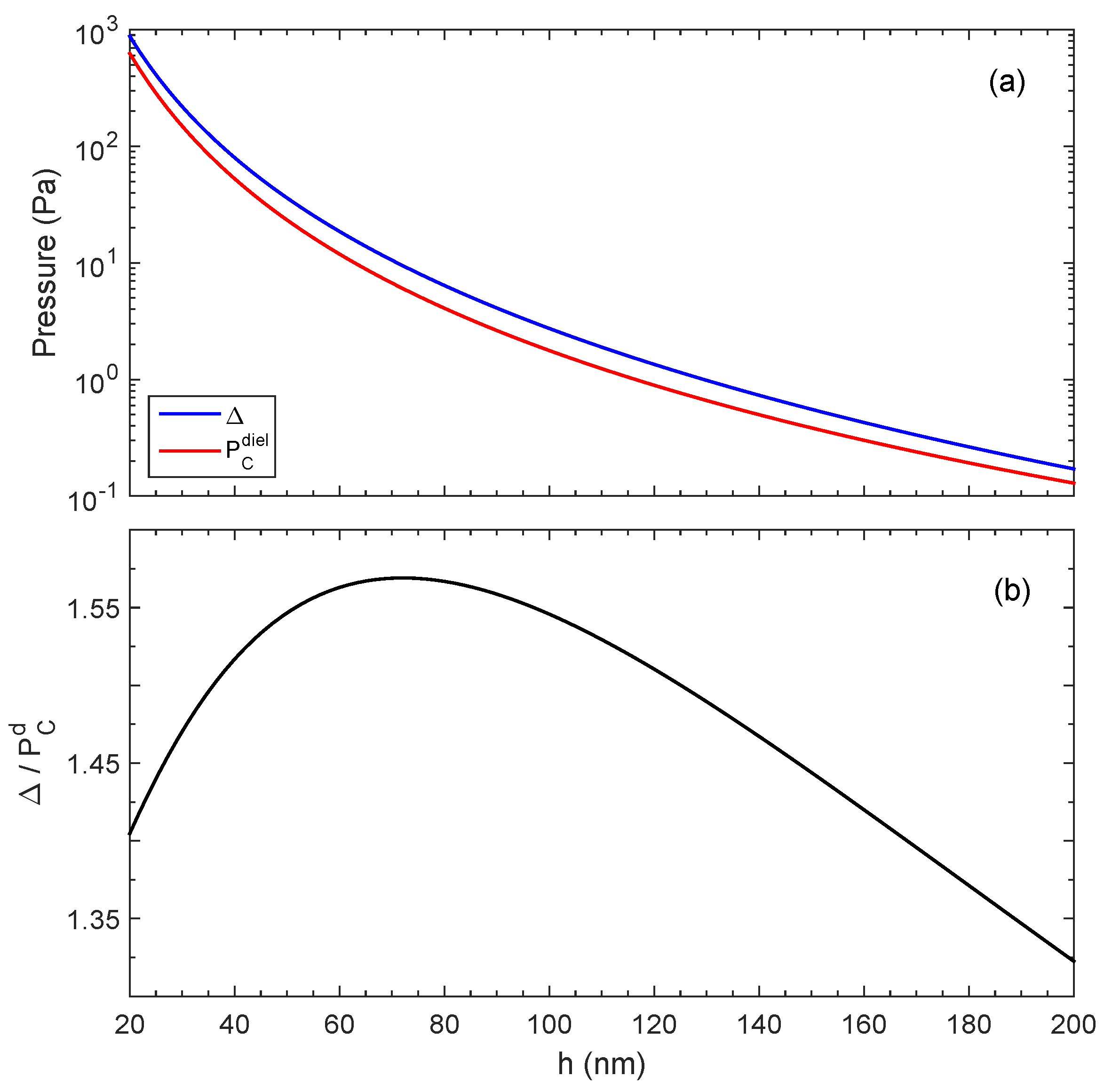
The pressure difference can be compared with the pressure between the metal and bulk dielectric as shown in Figure 3. Naively, one could expect that the difference, Δ = P C m / d P C m , is the pressure between the dielectric membrane with the thickness d and the metal. Figure 3a shows that this is not the case since the pressure, P C d , between the metal and bulk dielectric is even smaller than Δ . One can also see from Equation (16) that Δ does not coincide with the pressure between the dielectric membrane and metal. The difference, Δ , still keeps information about the underlying metal. Nevertheless, the contribution of the dielectric layer to Δ is significant, as one can see in Figure 3b, which shows the ratio, Δ / P C d , as a function of the distance, h.
The effect of the dielectric layer is reduced with its thickness and, for successful experiments, one has to keep the balance between the increasing compensating voltage and the increasing influence of the dielectric layer on the increase in its thickness. To some degree, one can influence the charge in the dielectric by plasma treatment or UV (ultra-violet) irradiation. The less the charge, the thicker the layer of the dielectric that can be used. Note that the thickness of the layer can be well characterized ellipsometrically. It is worth mentioning that the dielectric layer contributes significantly even at rather large distances. For example, at h = 200 nm, the relative contribution of the layer (see Equation (14)) is Δ R = 0.352 and, at h = 2000 nm, it is 0.054.

4. Conclusions

The total force measured experimentally includes a significant contribution from the electrostatic force that has to be separated from the Casimir force. When the force is measured between metals, the problem is solved by applying the compensating potential. The same method cannot be applied to dielectrics, for which the electrostatic force is strong due to the charging effect. The main idea of this paper was to use, instead of a bulk dielectric, a thin layer deposited on a metallic (or metallized) substrate. If the dielectric layer is sufficiently thin, the electrostatic force can be compensated for by applying an extra voltage to the metallic substrates. For a layer thickness above 100 nm, the compensating voltage becomes above 1 V, which is too large for practical use.
At the same time, at separations smaller than or of the order of 100 nm, a dielectric layer thicker than 10 nm contributes significantly to the Casimir force between a metal and the other metal covered with the dielectric. There is an optimal thickness of the layer such that the electrostatic force can be compensated for, but the contribution of the layer to the Casimir force is sufficient to extract information about the Casimir interaction of the metal with the bulk dielectric.
The main idea proposed in this paper can be generalized to the interaction of two dielectrics but, physically, an even more interesting case is the interaction of a semiconductor with metal.

Funding

This research was funded by the Ministry of Education and Science of the Russian Federation.

Data Availability Statement

Not applicable.

Conflicts of Interest

The author declares no conflict of interest.

References

  1. Casimir, H.B.G. On the attraction between two perfectly conducting plates. Proc. Kon. Ned. Akad. Wetensch. 1948, 51, 793–795. Available online: https://dwc.knaw.nl/DL/publications/PU00018547.pdf (accessed on 9 July 2023).
  2. Klimchitskaya, G.L.; Mohideen, U.; Mostepanenko, V.M. The Casimir force between real materials: Experiment and theory. Rev. Mod. Phys. 2009, 81, 1827–1885. [Google Scholar] [CrossRef] [Green Version]
  3. Rodriguez, A.W.; Capasso, F.; Johnson, S.G. The Casimir effect in microstructured geometries. Nat. Photon. 2011, 3, 211–221. [Google Scholar] [CrossRef]
  4. Mostepanenko, V.M. Casimir puzzle and Casimir conundrum: Discovery and search for resolution. Universe 2021, 7, 84. [Google Scholar] [CrossRef]
  5. Lu, B.S. The Casimir effect in topological matter. Universe 2021, 7, 237. [Google Scholar] [CrossRef]
  6. Harris, B.W.; Chen, F.; Mohideen, U. Precision measurement of the Casimir force using gold surfaces. Phys. Rev. A 2000, 62, 052109. [Google Scholar] [CrossRef] [Green Version]
  7. Chan, H.B.; Aksyuk, V.A.; Kleiman, R.N.; Bishop, D.J.; Capasso, F. Quantum mechanical actuation of microelectromechanical systems by the Casimir force. Science 2001, 291, 1941–1944. [Google Scholar] [CrossRef] [Green Version]
  8. Decca, R.S.; López, D.; Fischbach, E.; Krause, D.E. Measurement of the Casimir force between dissimilar metals. Phys. Rev. Lett. 2003, 91, 050402. [Google Scholar] [CrossRef] [Green Version]
  9. Decca, R.; López, D.; Fischbach, E.; Klimchitskaya, G.; Krause, D.; Mostepanenko, V. Precise comparison of theory and new experiment for the Casimir force leads to stronger constraints on thermal quantum effects and long-range interactions. Ann. Phys. 2005, 318, 37–80. [Google Scholar] [CrossRef] [Green Version]
  10. Lifshitz, E.M. The theory of molecular attractive forces between solids. Sov. Phys. JETP 1956, 2, 73–83. Available online: http://jetp.ras.ru/cgi-bin/e/index/e/2/1/p73?a=list (accessed on 9 July 2023).
  11. Dzyaloshinskii, I.E.; Lifshitz, E.M.; Pitaevskii, L.P. General theory of van der Waals’ forces. Sov. Phys. Uspekhi 1961, 4, 153–176. [Google Scholar] [CrossRef]
  12. Iannuzzi, D.; Lisanti, M.; Capasso, F. Effect of hydrogen-switchable mirrors on the Casimir force. Proc. Natl. Acad. Sci. USA 2004, 101, 4019–4023. [Google Scholar] [CrossRef]
  13. Chen, F.; Klimchitskaya, G.L.; Mostepanenko, V.M.; Mohideen, U. Demonstration of optically modulated dispersion forces. Opt. Express 2007, 15, 4823–4829. [Google Scholar] [CrossRef] [PubMed] [Green Version]
  14. de Man, S.; Heeck, K.; Wijngaarden, R.J.; Iannuzzi, D. Halving the Casimir force with conductive oxides. Phys. Rev. Lett. 2009, 103, 040402. [Google Scholar] [CrossRef] [PubMed] [Green Version]
  15. Torricelli, G.; van Zwol, P.J.; Shpak, O.; Binns, C.; Palasantzas, G.; Kooi, B.J.; Svetovoy, V.B.; Wuttig, M. Switching Casimir forces with phase-change materials. Phys. Rev. A 2010, 82, 010101. [Google Scholar] [CrossRef] [Green Version]
  16. Chang, C.C.; Banishev, A.A.; Klimchitskaya, G.L.; Mostepanenko, V.M.; Mohideen, U. Reduction of the Casimir force from Indium tin oxide film by UV treatment. Phys. Rev. Lett. 2011, 107, 090403. [Google Scholar] [CrossRef] [Green Version]
  17. Banishev, A.A.; Chang, C.C.; Castillo-Garza, R.; Klimchitskaya, G.L.; Mostepanenko, V.M.; Mohideen, U. Modifying the Casimir force between indium tin oxide film and Au sphere. Phys. Rev. B 2012, 85, 045436. [Google Scholar] [CrossRef] [Green Version]
  18. Banishev, A.A.; Klimchitskaya, G.L.; Mostepanenko, V.M.; Mohideen, U. Demonstration of the Casimir force between ferromagnetic surfaces of a Ni-coated sphere and a Ni-coated plate. Phys. Rev. Lett. 2013, 110, 137401. [Google Scholar] [CrossRef] [Green Version]
  19. Banishev, A.A.; Klimchitskaya, G.L.; Mostepanenko, V.M.; Mohideen, U. Casimir interaction between two magnetic metals in comparison with nonmagnetic test bodies. Phys. Rev. B 2013, 88, 155410. [Google Scholar] [CrossRef] [Green Version]
  20. van Zwol, P.J.; Palasantzas, G.; van de Schootbrugge, M.; De Hosson, J.T.M. Measurement of dispersive forces between evaporated metal surfaces in the range below 100 nm. Appl. Phys. Lett. 2008, 92, 054101. [Google Scholar] [CrossRef]
  21. Sedighi, M.; Svetovoy, V.B.; Palasantzas, G. Casimir force measurements from silicon carbide surfaces. Phys. Rev. B 2016, 93, 085434. [Google Scholar] [CrossRef]
  22. van Zwol, P.J.; Palasantzas, G.; De Hosson, J.T.M. Influence of random roughness on the Casimir force at small separations. Phys. Rev. B 2008, 77, 075412. [Google Scholar] [CrossRef] [Green Version]
  23. Broer, W.; Palasantzas, G.; Knoester, J.; Svetovoy, V.B. Roughness correction to the Casimir force at short separations: Contact distance and extreme value statistics. Phys. Rev. B 2012, 85, 155410. [Google Scholar] [CrossRef] [Green Version]
  24. Sushkov, A.O.; Kim, W.J.; Dalvit, D.A.R.; Lamoreaux, S.K. Observation of the thermal Casimir force. Nat. Phys. 2011, 7, 230–233. [Google Scholar] [CrossRef] [Green Version]
  25. Liu, M.; Xu, J.; Klimchitskaya, G.L.; Mostepanenko, V.M.; Mohideen, U. Precision measurements of the gradient of the Casimir force between ultraclean metallic surfaces at larger separations. Phys. Rev. A 2019, 100, 052511. [Google Scholar] [CrossRef] [Green Version]
  26. Bimonte, G.; López, D.; Decca, R.S. Isoelectronic determination of the thermal Casimir force. Phys. Rev. B 2016, 93, 184434. [Google Scholar] [CrossRef] [Green Version]
  27. Bimonte, G.; Spreng, B.; Maia Neto, P.A.; Ingold, G.L.; Klimchitskaya, G.L.; Mostepanenko, V.M.; Decca, R.S. Measurement of the Casimir force between 0.2 and 8 um: Experimental procedures and comparison with theory. Universe 2021, 7, 93. [Google Scholar] [CrossRef]
  28. Chen, F.; Klimchitskaya, G.L.; Mostepanenko, V.M.; Mohideen, U. Control of the Casimir force by the modification of dielectric properties with light. Phys. Rev. B 2007, 76, 035338. [Google Scholar] [CrossRef] [Green Version]
  29. Wu, Y.H.; Zha, J.W.; Li, W.K.; Wang, S.J.; Dang, Z.M. A remarkable suppression on space charge in isotatic polypropylene by inducing the beta-crystal formation. Appl. Phys. Lett. 2015, 107, 112901. [Google Scholar] [CrossRef]
  30. Xing, Z.; Zhang, C.; Cui, H.; Hai, Y.; Wu, Q.; Min, D. Space charge accumulation and decay in dielectric materials with dual discrete traps. Appl. Sci. 2019, 9, 4253. [Google Scholar] [CrossRef] [Green Version]
  31. Derjaguin, B. Untersuchungen über die Reibung und Adhäsion, IV. Kolloid-Zeitschrift 1934, 69, 155–164. [Google Scholar] [CrossRef]
  32. Derjaguin, B.V.; Abrikosova, I.I.; Lifshitz, E.M. Direct measurement of molecular attraction between solids separated by a narrow gap. Quart. Rev. 1968, 10, 295–329. [Google Scholar] [CrossRef]
  33. Zhou, F.; Spruch, L. Van der Waals and retardation (Casimir) interactions of an electron or an atom with multilayered walls. Phys. Rev. A 1995, 52, 297–310. [Google Scholar] [CrossRef]
  34. Svetovoy, V.B.; van Zwol, P.J.; Palasantzas, G.; De Hosson, J.T.M. Optical properties of gold films and the Casimir force. Phys. Rev. B 2008, 77, 035439. [Google Scholar] [CrossRef] [Green Version]
  35. Palik, E.D. (Ed.) Handbook of Optical Constants of Solids; Academic Press, Inc.: San Diego, CA, USA, 1985. [Google Scholar] [CrossRef]
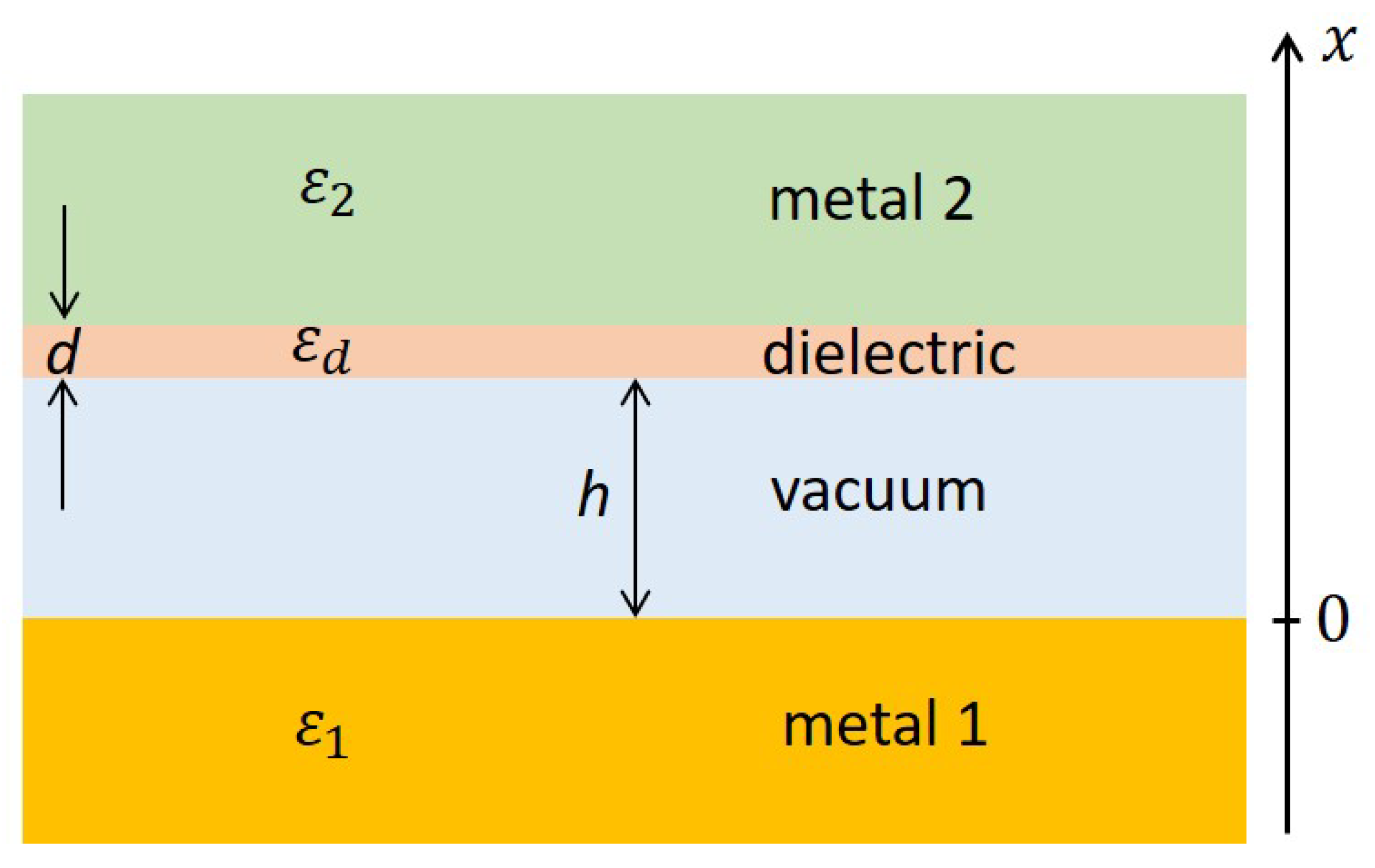
Figure 1. The structure under investigation. The plates are separated by a vacuum gap, h, and the thickness of the dielectric layer on one of the metals is d. The relative dielectric functions ( ε 1 , 2 ) of the materials are indicated; they are needed to calculate the Casimir attraction in this structure.
Physics 05 00051 g001
Figure 2. (a) Casimir pressure between two Au plates, one of which is covered by the SiO 2 layer with the thickness d. (b) Difference between the pressures with the dielectric layer and without it related to the pressure between bare metallic plates.
Physics 05 00051 g002
Figure 3. (a) Difference between pressures, Δ = P C m / d P C m (blue curve), and the pressure, P C d , between Au and bulk SiO 2 (red curve). In P C m / d , the thickness of the dielectric is d = 40 nm. (b) Ratio of the pressures presented in (a). The ratio shows that Δ carries significant information about the metal–dielectric interaction.
Physics 05 00051 g003
Disclaimer/Publisher’s Note: The statements, opinions and data contained in all publications are solely those of the individual author(s) and contributor(s) and not of MDPI and/or the editor(s). MDPI and/or the editor(s) disclaim responsibility for any injury to people or property resulting from any ideas, methods, instructions or products referred to in the content.