1. Introduction
The radiation-induced defects lead to an increase in the leakage current of silicon-based detectors. This current, also known as dark current or generation current, originates from carrier generation at radiation-induced defect levels. For gamma-irradiated silicon, it has been shown that the magnitude of the dark current depends on the oxygen concentration in the material and exhibits a quadratic dependence on the absorbed dose, or photon fluence [
1].
With the growing use of SiPMs as a convenient alternative to traditional Photomultiplier tubes, it is imperative that the effects of irradiation on the sensors are well explored. To date, numerous studies have investigated this [
1,
2,
3]. Extensive radiation hardness tests have been conducted on SiPMs for major experimental programs, as well as by SiPM manufacturers themselves [
4,
5,
6] demonstrating both the capabilities and the limitations of currently available SiPM technologies [
2,
7]. However, the majority of these investigations have been performed on non-working devices. In such studies, SiPMs are typically passively irradiated up to the maximum expected for the relevant experiment’s lifetime (often up to
or
) and their characteristics are sometimes measured weeks or months after the irradiation process. As a result, the effects of radiation on SiPMs during active operation remain insufficiently explored. Furthermore, the process of annealing has been shown to undo some of the displacement damage to silicon, even at room temperature [
3,
8] and gaps between irradiation and measurement allow for this effect to become significant—a scenario, which might not be relevant for many experiments. Nevertheless, these studies consistently report significant degradation of key parameters following proton and neutron irradiation, particularly at fluences exceeding
[
9].
While the general irradiation effect is consistent, quantitative results differ across experiments due to variations in device geometry, active area, manufacturing technology, and irradiation conditions. This emphasizes the need for systematic and comparative investigations. The present work investigates the effects of radiation on SiPMs that are powered and operating at nominal bias during the irradiation process and examines whether their behavior differs from what has been reported in previous studies conducted on non-operating devices, similarly to [
7]. Such studies remain limited and experimental verification is required. The investigated sensors include SiPMs manufactured by OnSemi (Scottsdale, AZ, USA) (later abbreviated as ONS) and FBK (Povo, Italy).
2. Materials and Methods
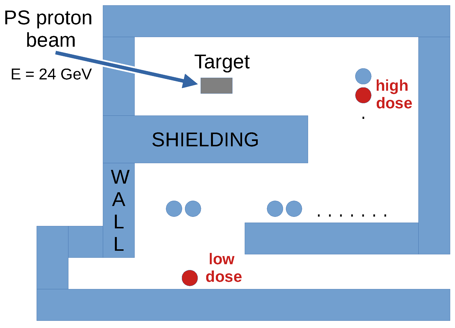
In this study, SiPMs were exposed to a non-uniform radiation field at the CHARM facility at CERN. A 24-GeV proton beam from the CERN PS is directed at a copper or aluminium target. Secondary non-uniform radiation is created from the target, and different dose intensities and dose types can be achieved by placing a setup at different points in the irradiation area. The full layout of the facility is shown in
Figure 1.
Two identical SiPM test setups were irradiated. Each consisted of a light-tight box within which a number of components were fitted:
6 PCBs housing the SiPMs and their readout circuits (Shown in
Figure 2);
A PCB housing LEDs for pulse characteristics studies;
A base PCB, housing the SiPM PCBs, and the cabling and connections to the outside of the box.
The two setups were placed at different locations within the irradiation facility, resulting in different irradiation levels. One was at the G0 irradiation point, marked as “low dose” in
Figure 1. This is the lowest dose location in the irradiation region of the facility. The other was on the irradiation rack which is very close to the beam axis, and is marked as “high dose” on
Figure 1. The use of both of these locations for the irradiation allows for comparing different final doses and accumulation rates between the two setups.
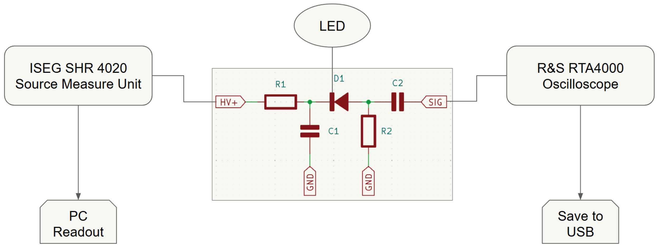
A schematic of the readout is presented in
Figure 2. The signal from the SiPM is fed directly into the oscilloscope with no amplification applied. An LED powered by a pulse generator was used to shine light on the SiPMs, enabling signal collection. The ISEG SHR 4020 SMU [
10] acted as both a power supply for biasing the SiPMs and a measurement device for the currents, allowing us to obtain I-V curves mid-irradiation.
Figure 2.
A schematic representation of the readout setup [
11]. The Biasing resistor R1 is 10 kΩ, the load resistor R2 is 1 kΩ, the decoupling capacitor C1 is 10 nF, and the coupling capacitor C2 is 100 pF. D1 represents a SiPM.
Figure 2.
A schematic representation of the readout setup [
11]. The Biasing resistor R1 is 10 kΩ, the load resistor R2 is 1 kΩ, the decoupling capacitor C1 is 10 nF, and the coupling capacitor C2 is 100 pF. D1 represents a SiPM.
Three different types of SiPMs were tested:
MICROFJ-30035-TSV—Produced by OnSemi. 3 × 3 mm2 active area, 5676 total microcells, 35 μm pixel size, typical breakdown voltage −24.5 V;
ASD-RGB3S-P-40—Produced by FBK. 3 × 3 mm2 active area, 5520 total microcells, 40 μm pixel size, typical breakdown voltage −27.0 V;
ASD-RGB4S-P-40—Produced by FBK. 4 × 4 mm2 active area, 9340 total microcells, 40 μm pixel size, typical breakdown voltage −27.0 V.
Per box there were two samples of each SiPM type. One of each pair would remain biased at 2.5 V overvoltage, while the other was irradiated passively. This setup aimed to test whether the state of the SiPM during the irradiation affects response degradation. The SiPM response was measured before irradiation, so that a reference is available. After the start of irradiation, the measurement procedure was as follows:
- 1.
The powered SiPMs were ramped down to 5 V below breakdown voltage. This state was recorded for 2–3 min;
- 2.
A slow ramp (0.2 V/s) was initiated back to 2.5 V overvoltage;
- 3.
The max overvoltage state was maintained and recorded for further 2–3 min, so that the SiPMs had time to stabilise;
- 4.
The LED pulser was turned on, and the signal shapes were recorded using the oscilloscope;
- 5.
LED pulser was turned off to prepare for the measurement of the remaining samples;
- 6.
The non-powered SiPM samples were ramped up to 5 V below breakdown voltage;
- 7.
The same measurement procedure (steps 2, 3, 4, and 5) was performed for them;
- 8.
The passive samples and LED were powered off. The other half of the samples remained at 2.5 V overvoltage.
3. Results
The measurement procedure was repeated 2–3 times per day, for a total irradiation time of 5 days. The measurement periods were the only times when the SiPMs would spend time out of their “assigned” state, as the powered samples would be brought below overvoltage to prepare for measurements, while the passive ones would need to be powered during the measurements themselves. This aims to address a gap in the literature, where most tests are performed with the SiPMs irradiated passively, and the actual measurements on them performed weeks or even months after, allowing room-temperature annealing to affect the results.
A total of 15 measurements were performed during the period, with measurement 0 being the baseline point before irradiation, 1–11 being the intermittent measurements, and 12–14 having been performed directly after the irradiation was stopped, but before removal from the irradiation room.
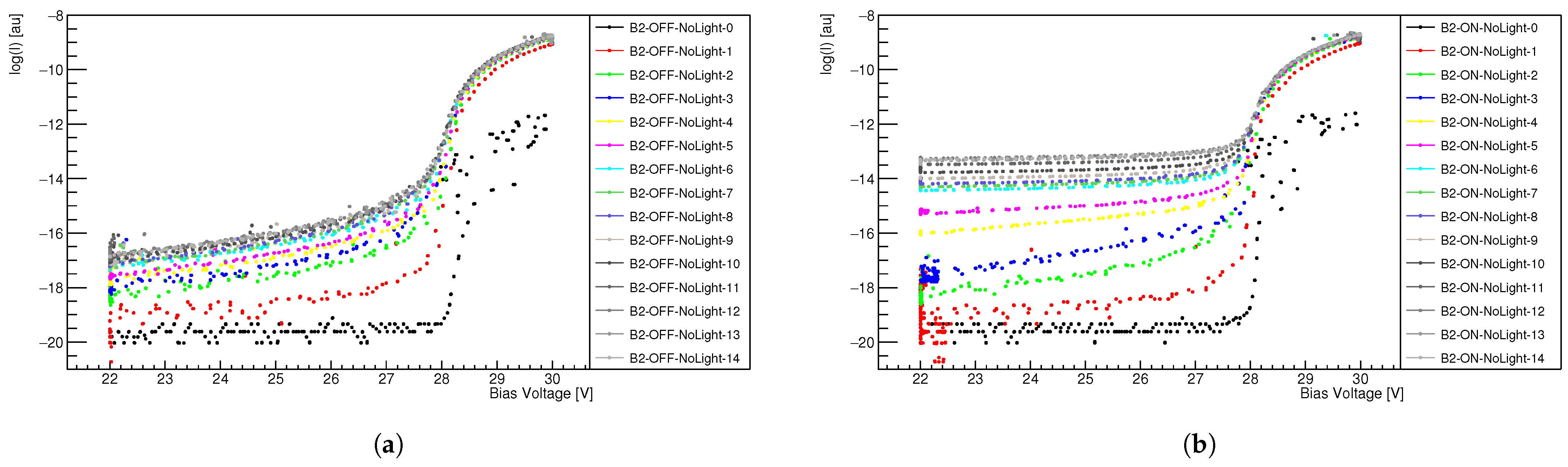
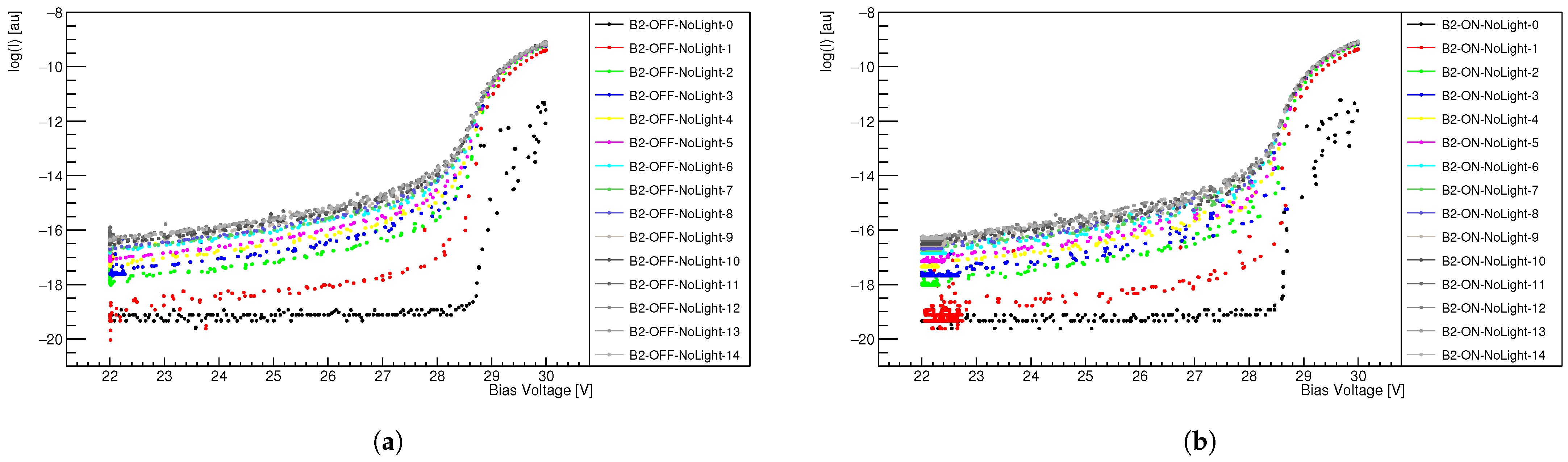
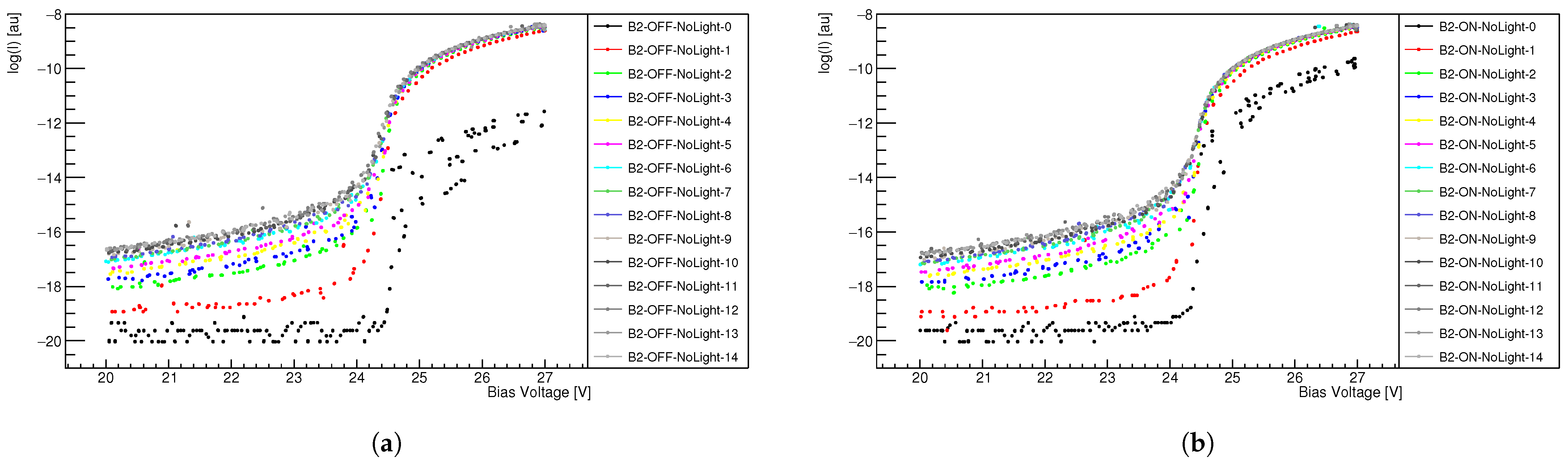
The I-V curves for the SiPMs placed in the high dose point are presented in
Figure 3,
Figure 4 and
Figure 5. The legend strings are interpreted as follows: B2—Refers to SiPM placed at the High Radiation point; ON/OFF—Actively/Passively irradiated SiPM; NoLight—I-V curve is pure dark current without LED light; Number at the end—the measurement sequence.
The behaviour of the I-V curves is as expected, with both the final current and the leakage current before breakdown rising as the irradiation progresses. The change is most noticeable for the first couple of dose points, after which the I-V curves cluster together, hinting at some sort of saturation. There is a noticeable change in I-V curve shape for the FBK-3x3-ON SiPM, where the leakage current before breakdown rises significantly with radiation, however the other samples do not exhibit such behaviour, including the 4 × 4 SiPM of the same make, leading to the conclusion that this result is more probably something in the electronics, rather than a physical result.
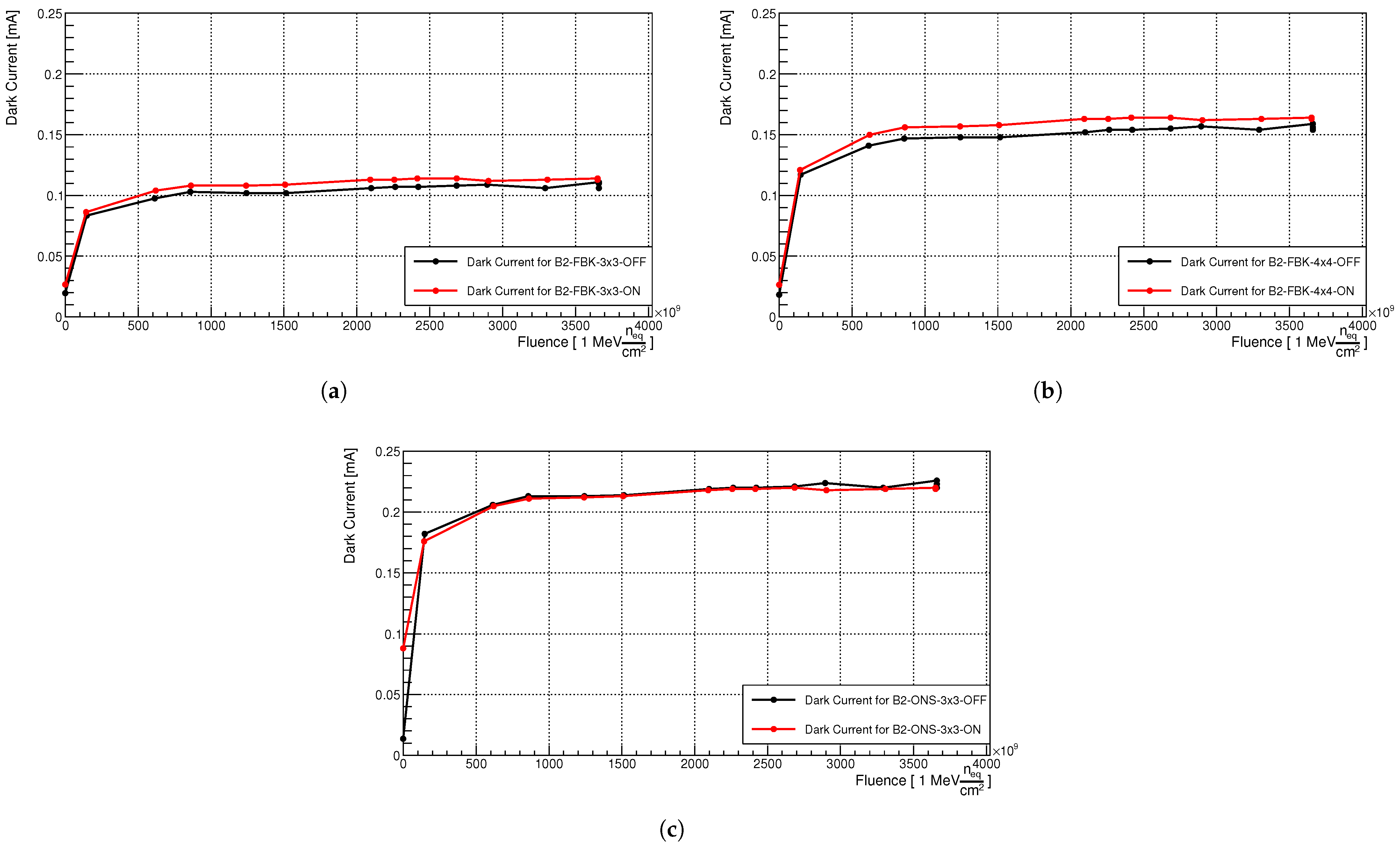
Figure 6 presents plots of the dark current at 2.5 V overvoltage as a function of the accumulated fluence. Again, B2 in the legend string refers to the high radiation point, while ON/OFF differentiates the actively and passively irradiated SiPMs. The final 3 points, taken after the irradiation are used as an estimate of the uncertainty of the measurements, which accounts to 5%. The final currents end up at about an order of magnitude higher than the baseline. Curiously, two of the SiPMs exhibit a systematic difference between the final currents for the active and the passive irradiation, with the current for the actively irradiated SiPM being 7–8 % higher.
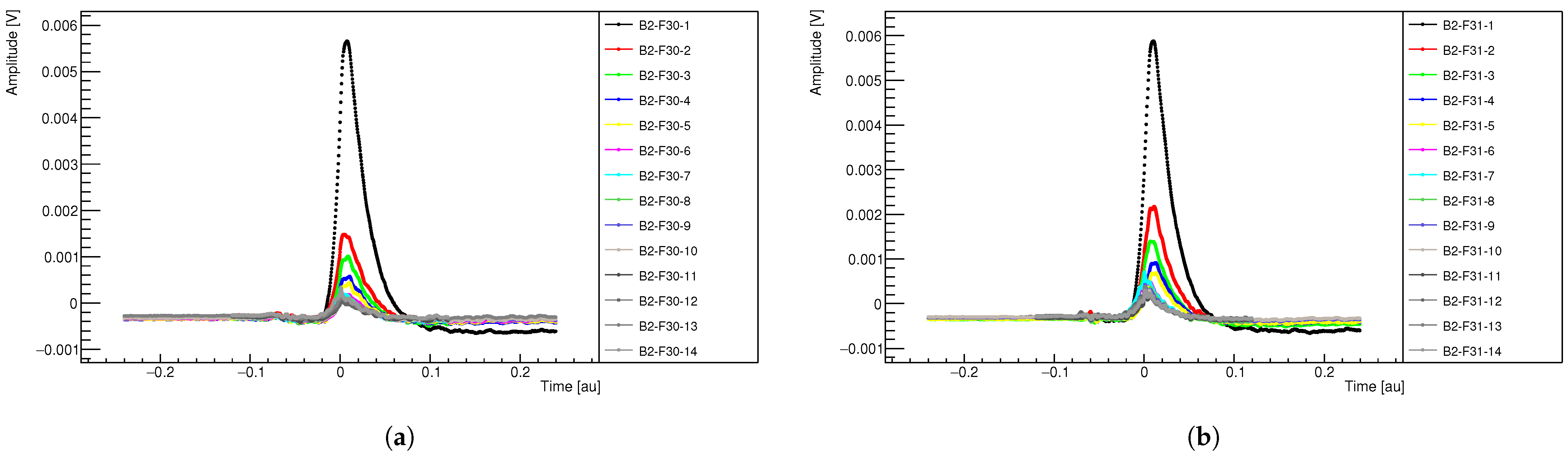
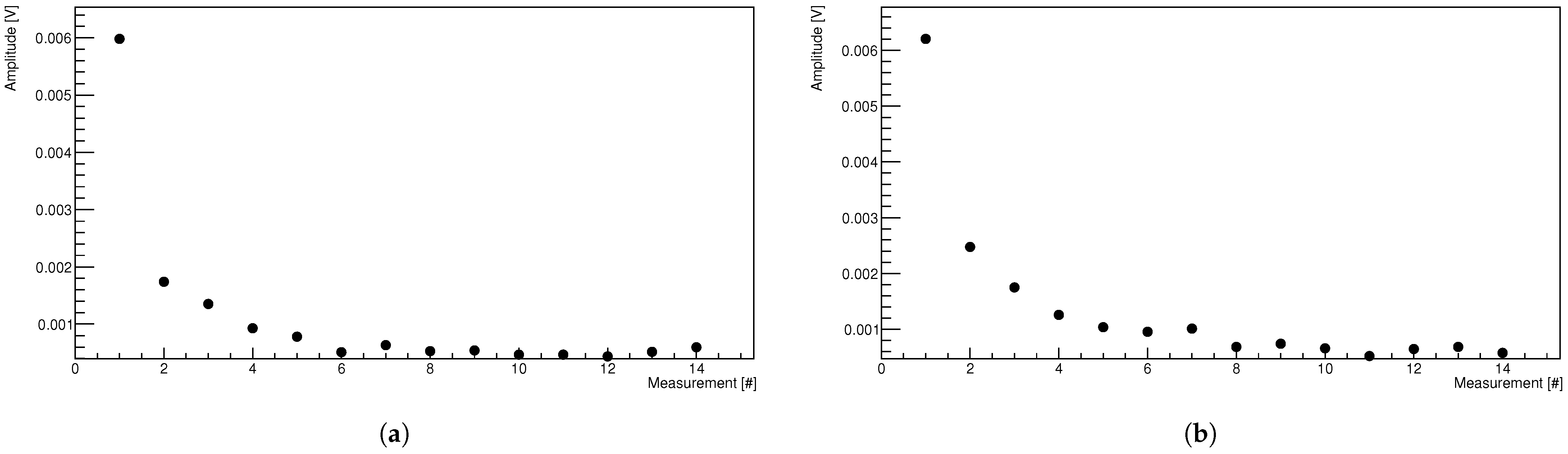
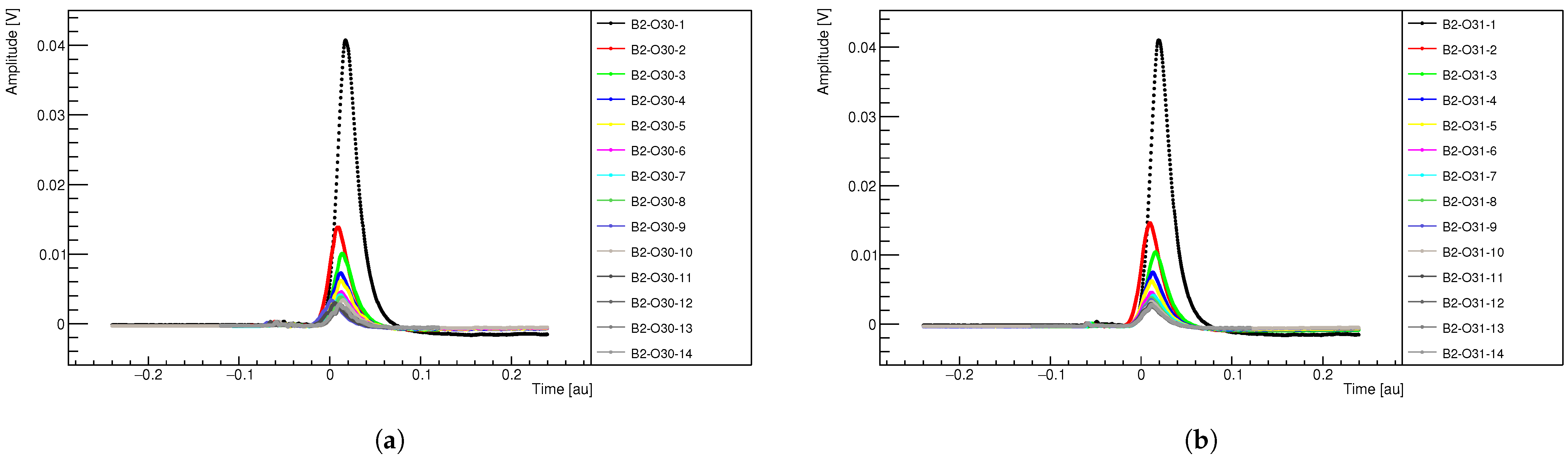
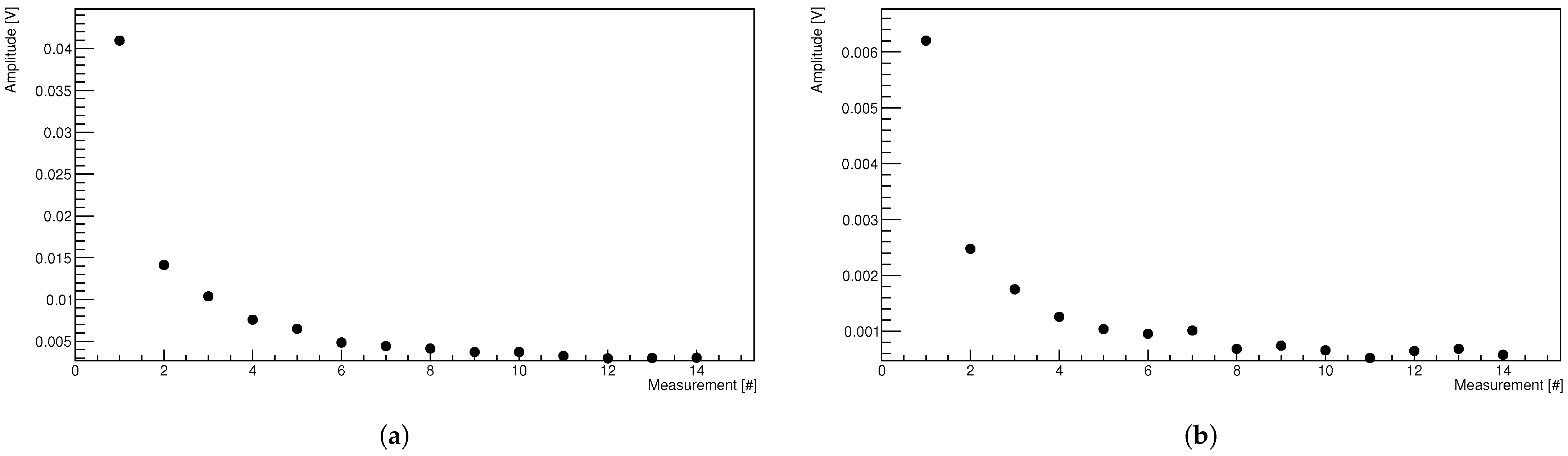
Figure 7,
Figure 8,
Figure 9 and
Figure 10 present the evolution of the signal shapes and max amplitudes with subsequent measurements for the
mm
2 FBK and ONS SiPMs. Signal data for the
mm
2 FBK SiPMs is not available. Legend string here is constructed differently, with B2 and the trailing number preserving their meaning, however the central substring uses the letters F/O to denote FBK or ONS, then the numbers 3/4 denote the active area (
or
mm
2), and finally the numbers 1/0 denote active or passive irradiation.
There is a drop in the observed amplitude by about one order of magnitude and a distortion of the shapes of the signals as the irradiation progresses. The loss of amplitude can be attributed to the combination of the 1 kΩ load resistor, and the coupling capacitor C2 to the oscilloscope. When measuring signals through the oscilloscope, the current needs to be replenished. However, with the C2 capacitor being present, this replenishment can only happen through the R2 resistor, leading to a voltage drop in the circuit and effective loss of overvoltage for the SiPM. This process results in suppression of the SiPM gain with increase of the current, as the voltage drop on R2 increases as well. So while during the initial measurements the suppression effect is negligible, with the rising current after irradiation, its contribution increased substantially.
4. Discussion
As also seen in the literature, the current rises sharply with irradiation, the dark current increasing by more than an order of magnitude. The main evolution is observed for fluences up to
, after which the current saturates and a plateau forms. During the analysis it was noted that the current is strongly limited by the use of a high value biasing resistor—the 10 kΩ R1 (
Figure 2). Later measurements showed that substituting this resistor with a 25 Ω one affects the measured dark current by about one order of magnitude. Specifically, there was a 6.8 times increase for the
FBK SiPM, 7 times increase for the FBK
SiPM, and 8.6 times for the OnSemi SiPM. The current curves in
Figure 11 show the observed currents for the passively irradiated SiPM after this resistor change.
In the passive versus active comparison in
Figure 6, the current curves for the ONS-MICROFJ-30035-TSV essentially overlap, and separation of the curves for both FBK samples is close to the uncertainty. The behaviour of passive versus active SiPMs is therefore inconclusive, and it is difficult to claim that there is a statistically significant effect visible. Curiously, where differences are observed, the active SiPM is the one exhibiting a higher current. The temperature in the irradiation room is controlled and expected to remain constant during the measurement period itself. Thus its effect on the comparison is minimal. Yet, the active SiPM stay heated by the passing currents during the periods when no measurements are being performed. This should lead to a temperature difference up to a couple of degrees Celsius between the active and passive samples, and a small additional annealing effect on the active SiPM, so lower final currents are expected.
During the measurements themselves both active and passive SiPM are powered, exhibiting similar currents (thus also similar heating). Breakdown voltage increases with temperature, thus effectively lowering the gain of the SiPM at a fixed voltage. With no direct temperature measurements available in the case of this study, this requires that the breakdown voltages themselves are extracted from the I-V curves, so that final currents can be properly normalized withing the analysis, if any fluctuations are present.
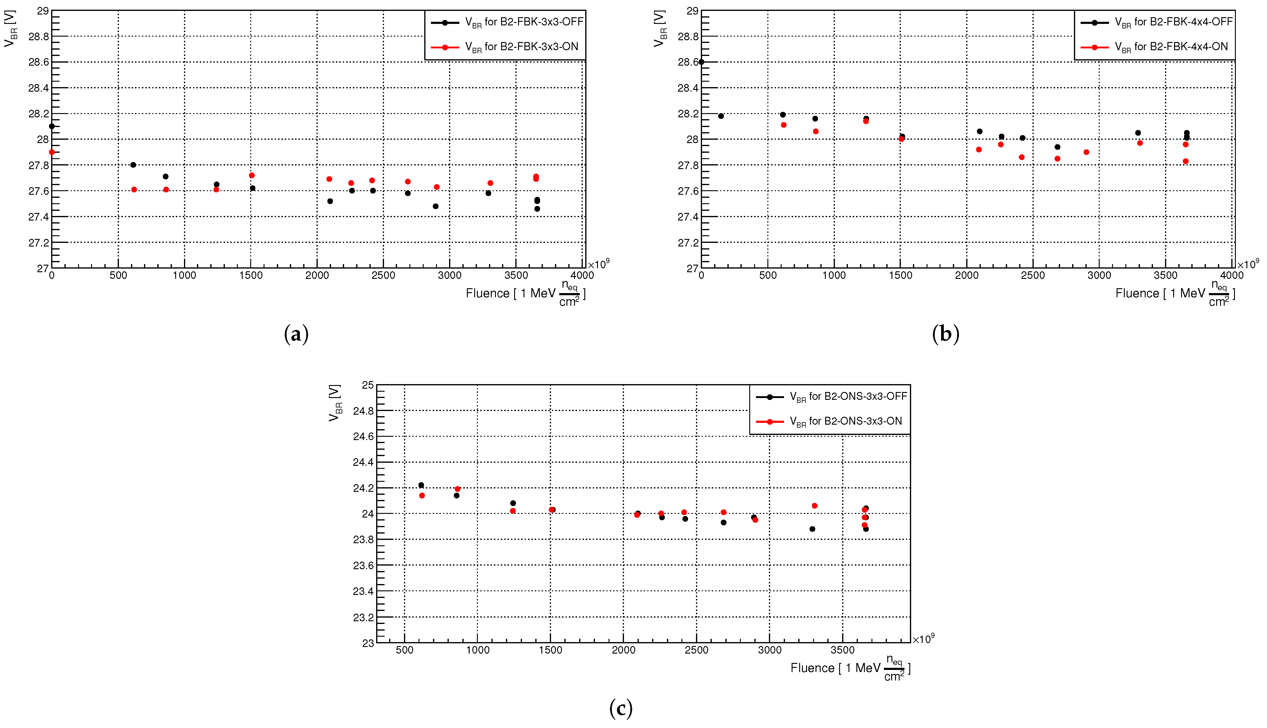
As seen in
Figure 12, slight changes of the breakdown voltages were consistently observed for all SiPM types, especially after the first measurement (where the samples were moved into the irradiation area).
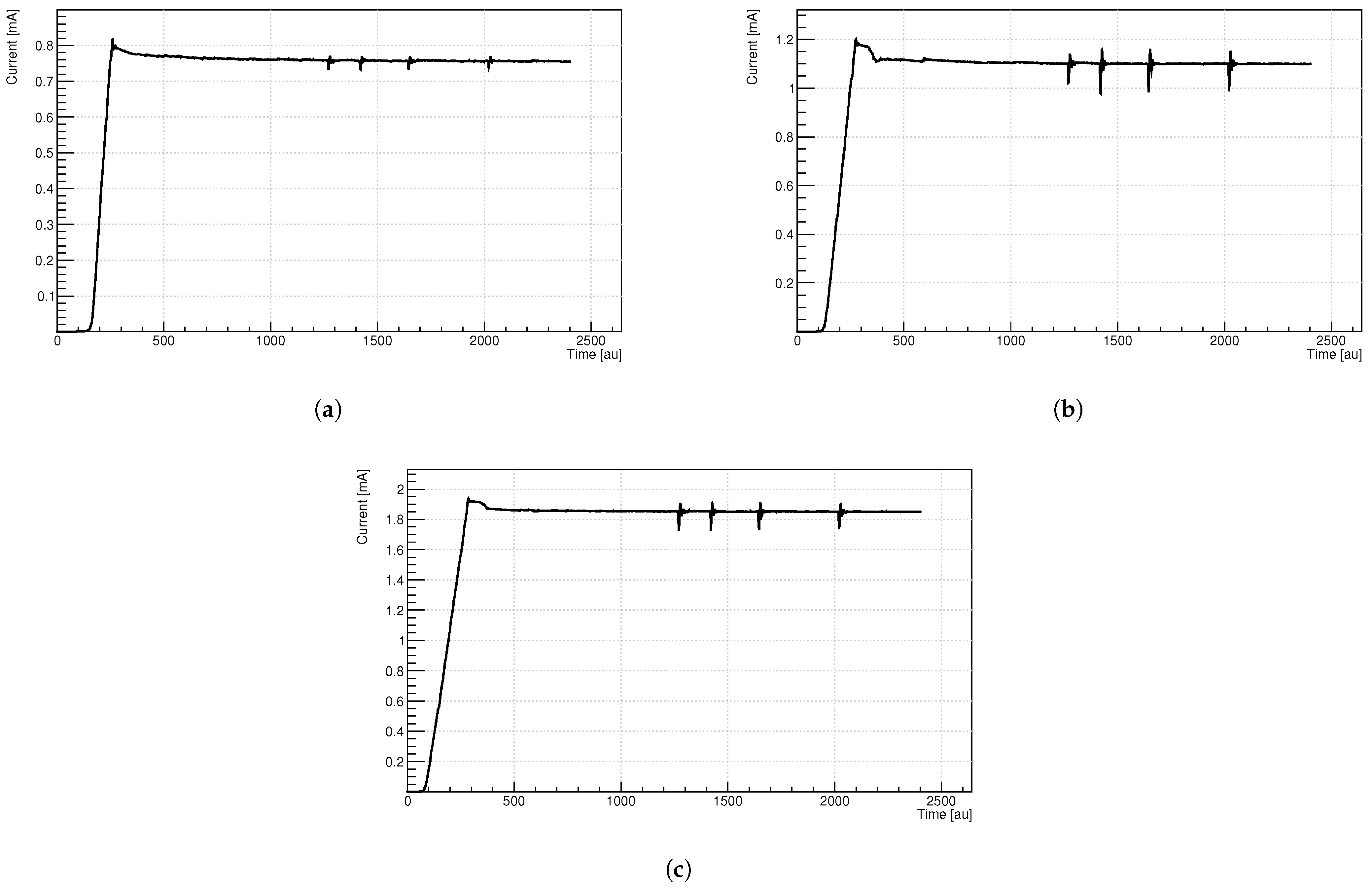
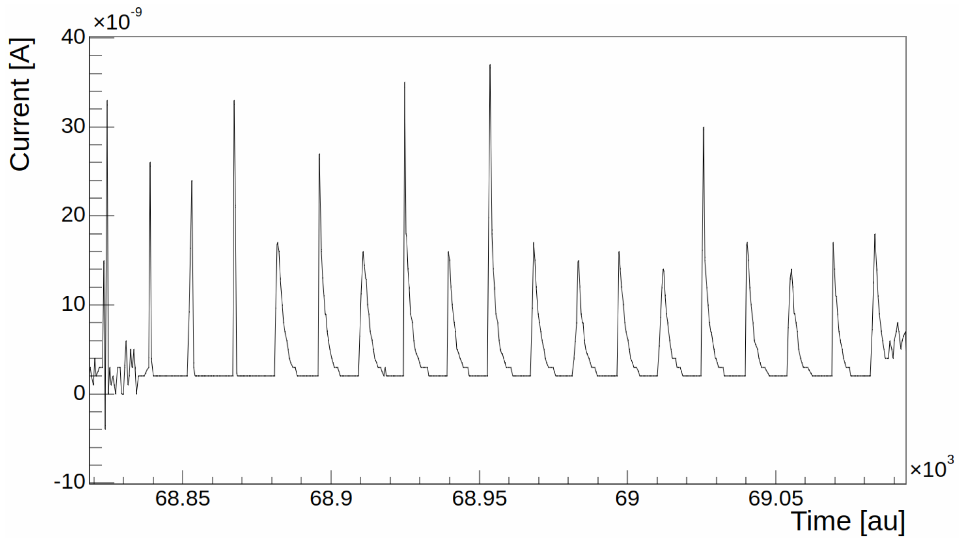
Another effect that should be considered is the influence of the beam itself. As the measurements for this study were performed during active irradiation, it is reasonable to assume that the beam hitting the SiPMs might be generating some additional current through the sensors. This effect is, however, shown to be minimal.
Figure 13 shows the beam bunches in a current as a function of time graph. Each bunch is roughly equivalent to a fluence of
. The visible peaks are extremely short, and in the range of tens of nanoamperes, making them negligible in comparison to the currents in the order of hundreds of microamps measured after the sensors have been irradiated.
Finally, as shown by the interaction between the R2 resistor and the C2 capacitor, which was described in the Results chapter, effects within the measurement electronics are likely affecting the data. Specifically in the case of signal measurements, the drop in amplitude is very likely a result of this R2-C2 setup. As such, a future measurement setup would need to eliminate this effect, in order to confirm the results. Measurements of the currents, however, do not make direct use of this part of the readout chain, and they are not affected by the same suppression effect. Nevertheless, the suppression from the R1 resistor is affecting those. And while the trends of increasing current with irradiation would not be strongly affected, and neither would the difference in performance between the separate SiPM models, removing this current suppression in a future study might help in establishing the statistical significance of how the passive or active irradiation truly affects degradation.
5. Conclusions
The current study focuses on the effect of the ionizing radiation on SiPMs operated at nominal voltage during the exposure. Three different types of SiPMs with different pixel size were irradiated up to dose of 500 Gy and fluence of about 1 MeV neq/cm2. The obtained I-V curves, dark current and pulse changes in the powered on and off samples are consistent and follow qualitatively the expectations, however, this does not directly reject the idea that SiPM state might affect its degradation during irradiation. Further and more precise studies are required with a slightly modified setup to avoid dark current saturation and with a better controlled temperature monitoring.
Author Contributions
Conceptualization, I.G.B., V.K. and Y.A.M.; methodology, V.B., Y.A.M. and V.K.; hardware, D.I. and V.B.; software, formal analysis, V.B.; writing—original draft preparation, V.B. and M.G.; writing—review and editing, V.K., I.G.B. and Y.A.M. All authors have read and agreed to the published version of the manuscript.
Funding
Ian G. Bearden acknowledges support from the The Carlsberg Foundation (CF21-0606) and the Danish Council for Independent Research/Natural Sciences. Sofia University team acknowledges support from the Bulgarian Ministry of Education and Science, within the National Roadmap for Research Infrastructures (object CERN) and by Project BG16RFPR002-1.014-0006 “National Centre of Excellence Mechatronics and Clean Technologies”. Valentin Buchakchiev acknowledges support from ESA through contract number 4000142764/23/NL/MH/rp.
Data Availability Statement
The datasets used to obtain the results in this study are available on request from the authors.
Conflicts of Interest
The authors declare no conflicts of interest. The funders had no role in the design of the study; in the collection, analyses, or interpretation of data; in the writing of the manuscript; or in the decision to publish the results.
References
- Moll, M. Displacement Damage in Silicon Detectors for High Energy Physics. IEEE Trans. Nucl. Sci. 2018, 65, 1561–1582. [Google Scholar] [CrossRef] [Scilit]
- Mikhaylov, V.; Guber, F.; Ivashkin, A.; Kugler, A.; Kushpil, V.; Morozov, S.; Svoboda, O.; Tlustý, P. Characterisation of SiPM radiation hardness for application in hadron calorimeters at FAIR, CERN and NICA. J. Instrum. 2020, 15, C02005. [Google Scholar] [CrossRef] [Scilit]
- Tsang, T. Silicon photomultipliers radiation damage and recovery via high temperature annealing. J. Instrum. 2018, 13, P10019. [Google Scholar] [CrossRef] [Scilit]
- Bychkova, O.; Parygin, P.; Garutti, E.; Kaminsky, A.; Martens, S.; Popova, E.; Schwandt, J.; Stifutkin, A. Radiation hardness study using SiPMs with single-cell readout. Nucl. Instrum. Methods Phys. Res. Sect. A Accel. Spectrometers Detect. Assoc. Equip. 2022, 1031, 166533. [Google Scholar] [CrossRef] [Scilit]
- Mazzi, A. SiPM development at FBK for highly irradiated environments. In Proceedings of the 30th International Workshop on Vertex Detectors, Oxford, UK, 27–30 September 2021. [Google Scholar]
- Gola, A.; Acerbi, F.; Ficorella, A.; Merzi, S.; Monreal, L.; Moretti, E.; Paternoster, G.; Penna, M.; Ruzzarin, M.; Zorzi, N. FBK R&D on rad-hard SiPMs. In Proceedings of the AIDAinnova WP8 Face-to-Face Meeting, Geneva, Switzerland, 11 January 2023. [Google Scholar]
- Curras, E.; Fernández, M.; Gallrapp, C.; Gray, L.; Mannelli, M.; Meridiani, P.; Moll, M.; Nourbakhsh, S.; Scharf, C.; Silva, P.; et al. Radiation hardness and precision timing study of silicon detectors for the CMS High Granularity Calorimeter (HGC). Nucl. Instrum. Methods Phys. Res. Sect. A Accel. Spectrometers Detect. Assoc. Equip. 2017, 845, 60–63. [Google Scholar] [CrossRef] [Scilit]
- De Angelis, N.; Kole, M.; Cadoux, F.; Hulsman, J.; Kowalski, T.; Kusyk, S.; Mianowski, S.; Rybka, D.; Stauffer, J.; Swakon, J.; et al. Temperature dependence of radiation damage annealing of Silicon Photomultipliers. Nucl. Instrum. Methods Phys. Res. Sect. A Accel. Spectrometers Detect. Assoc. Equip. 2023, 1048, 167934. [Google Scholar] [CrossRef] [Scilit]
- Altamura, A.R.; Acerbi, F.; Nociforo, C.; Regazzoni, V.; Mazzi, A.; Gola, A. Characterization of Silicon Photomultipliers after proton irradiation up to 1014 neq/cm2. Nucl. Instrum. Methods Phys. Res. Sect. A Accel. Spectrometers Detect. Assoc. Equip. 2022, 1040, 167284. [Google Scholar] [CrossRef] [Scilit]
- iseg Spezialelektronik GmbH. Technical documentation: SHR Switchable High Precision AC/DC Desktop High Voltage Power Supply. 2020. Available online: https://iseg-hv.com/download/AC_DC/SHR/archive/iseg_manual_SHR_en_2.0.pdf (accessed on 1 March 2026).
- Melikyan, Y.A.; Bearden, I.G.; Buchakchiev, V.; Jia, S.; Kozhuharov, V.; Møller, I.P. Characterization of the large-size NDL EQR20 silicon photomultipliers. Nucl. Instrum. Methods Phys. Res. Sect. A Accel. Spectrometers Detect. Assoc. Equip. 2025, 1078, 170604. [Google Scholar] [CrossRef] [Scilit]
Figure 1.
Schematic representation of the layout of the irradiation room at CHARM.
Figure 1.
Schematic representation of the layout of the irradiation room at CHARM.
Figure 3.
Evolution of the I-V curves with total fluence for the OnSemi mm2 SiPMs for: (a) Passively irradiated, (b) Actively irradiated.
Figure 3.
Evolution of the I-V curves with total fluence for the OnSemi mm2 SiPMs for: (a) Passively irradiated, (b) Actively irradiated.
Figure 4.
Evolution of the I-V curves with total fluence for the FBK mm2 SiPMs for: (a) Passively irradiated, (b) Actively irradiated.
Figure 4.
Evolution of the I-V curves with total fluence for the FBK mm2 SiPMs for: (a) Passively irradiated, (b) Actively irradiated.
Figure 5.
Evolution of the I-V curves with total fluence for the FBK mm2 SiPMs for: (a) Passively irradiated, (b) Actively irradiated.
Figure 5.
Evolution of the I-V curves with total fluence for the FBK mm2 SiPMs for: (a) Passively irradiated, (b) Actively irradiated.
Figure 6.
Current measured against total Fluence for the SiPMs placed at the high radiation point. (a) FBK mm2, (b) FBK mm2, (c) OnSemi mm2.
Figure 6.
Current measured against total Fluence for the SiPMs placed at the high radiation point. (a) FBK mm2, (b) FBK mm2, (c) OnSemi mm2.
Figure 7.
Evolution of the signal shapes with total fluence for the FBK mm2 SiPMs. (a) Passively irradiated, (b) Actively irradiated.
Figure 7.
Evolution of the signal shapes with total fluence for the FBK mm2 SiPMs. (a) Passively irradiated, (b) Actively irradiated.
Figure 8.
Evolution of the signal amplitudes with the measurement index for the FBK mm2 SiPMs. (a) Passively irradiated, (b) Actively irradiated.
Figure 8.
Evolution of the signal amplitudes with the measurement index for the FBK mm2 SiPMs. (a) Passively irradiated, (b) Actively irradiated.
Figure 9.
Evolution of the signal shapes with total fluence for the OnSemi mm2 SiPMs. (a) Passively irradiated, (b) Actively irradiated.
Figure 9.
Evolution of the signal shapes with total fluence for the OnSemi mm2 SiPMs. (a) Passively irradiated, (b) Actively irradiated.
Figure 10.
Evolution of the signal amplitudes with the measurement index for the OnSemi mm2 SiPMs. (a) Passively irradiated, (b) Actively irradiated.
Figure 10.
Evolution of the signal amplitudes with the measurement index for the OnSemi mm2 SiPMs. (a) Passively irradiated, (b) Actively irradiated.
Figure 11.
Current curves for the passively irradiated SiPMs after switching the R1 resistor to 25 Ohm. (a) FBK mm2, (b) FBK mm2, (c) OnSemi mm2.
Figure 11.
Current curves for the passively irradiated SiPMs after switching the R1 resistor to 25 Ohm. (a) FBK mm2, (b) FBK mm2, (c) OnSemi mm2.
Figure 12.
Changes in Breakdown Voltage for the SiPMs placed at the high radiation point. (a) FBK mm2, (b) FBK mm2, (c) OnSemi mm2.
Figure 12.
Changes in Breakdown Voltage for the SiPMs placed at the high radiation point. (a) FBK mm2, (b) FBK mm2, (c) OnSemi mm2.
Figure 13.
The current peaks corresponding to beam bunches passing through the setup.
Figure 13.
The current peaks corresponding to beam bunches passing through the setup.
| Disclaimer/Publisher’s Note: The statements, opinions and data contained in all publications are solely those of the individual author(s) and contributor(s) and not of MDPI and/or the editor(s). MDPI and/or the editor(s) disclaim responsibility for any injury to people or property resulting from any ideas, methods, instructions or products referred to in the content. |




 ,
,