Article

Impedance Spectroscopy of Hybrid Structures Based on Nanostructured Porous Silicon and Porous Hierarchical Nickel Oxide Nanoparticles


by
Kamilya Khalugarova
1,*,
Yulia M. Spivak
1,
Anton A. Bobkov
1,
Dmitriy A. Kozodaev
2 and
Vyacheslav A. Moshnikov
1
1
Department of Micro- and Nanoelectronics, Saint Petersburg Electrotechnical University “LETI”, Professora Popova St., 5, 197022 Saint Petersburg, Russia
2
NT-MDT BV, Hoenderparkweg 96 b, 7335 Apeldoorn, The Netherlands
*
Author to whom correspondence should be addressed.
Surfaces 2026, 9(3), 71; https://doi.org/10.3390/surfaces9030071
Submission received: 28 May 2026 / Revised: 19 July 2026 / Accepted: 29 July 2026 / Published: 4 August 2026

Abstract

A technological approach to the formation of a 3D nanocomposition material based on hierarchical porous nickel oxide nanoparticles incorporated into porous silicon with a dendritic porous structure is proposed. Porous silicon was used as a 3D porous template, in the presence of which porous hierarchical nickel oxide nanoparticles were synthesized using a “green” synthesis method followed by annealing in an oxygen-containing atmosphere. The resulting materials were characterized using scanning electron microscopy, transmission electron microscopy, X-ray spectral microanalysis, X-ray diffraction, and the BET method. The potential of a developed composition based on porous hierarchical nickel and silicon oxide nanoparticles to enhance the sensitivity of adsorption gas sensors was assessed using impedance spectroscopy in the presence of a probe gas (isopropanol). Gas sensitivity measurements were conducted at room and elevated temperatures in the frequency range from 100 Hz to 500 kHz. Differences in the dependences of the real part of impedance on the imaginary part were revealed for the porNiO-porSi composition in Nyquist coordinates. The results are discussed in terms of percolation theory and fractal organization.

1. Introduction

Currently, an effective way to enhance the properties of functional nanomaterials is to produce a proper design of its nanostructure, including its hierarchical structure, porous structure (micro-, meso-, macropores), fractalization, percolation, boundary design, and so on, tailored to a specific task [1,2,3,4]. From this point of view, two approaches are of interest: active atomic–molecular design and complex architectures that integrate multiple hierarchical levels with specific functional properties. First are the technological techniques used during the production and post-processing of materials to control the restructuring of the internal structure, taking into account the physicochemical processes occurring in such materials (oxidation, component diffusion, Kirkendall and Frenkel effects, etc.), resulting in unique material designs at the nanoscale with a specified degree of structural perfection, the required material doping profiles, variability, etc. Second, we have the incorporation and encapsulation of hierarchical porous matrices with nanomaterials of various natures and 0–3 dimensions (metallic nanoparticles, semiconductor colloidal quantum dots, carbon nanostructures, metal oxides, polymers, etc.). This allows us not only to combine the advantages of such nanomaterials but also to achieve synergistic effects when combining them at the nanoscale. This approach is aimed at developing a technological sequence of actions (including a sequence of different types of synthesis, pre- and post-processing, a combination of several types of nanomaterials, etc.) in such a way as to form a specific nanostructure with improved functional parameters [5,6,7,8,9,10].
Nickel oxide (NiO) has attracted attention due to its good chemical stability, as well as its optical and electrical properties [11,12]. NiO is a p-type semiconductor with a wide bandgap (3.6–4.0 eV), which makes it transparent in the visible wavelength range [13]. NiO finds application in various fields. In photovoltaics, NiO has proven to be an effective hole transport material [14], being used, for example, as hole injection and transport layers in organic light-emitting diodes [15]. In electronics, NiO is used as one of the key materials for the next generation of non-volatile memory [16]. The performance of NiO in many applications depends on its crystallinity, phase composition, size, and morphology. NiO nanoparticles with a well-developed porous structure are also widely used in energy storage devices, such as supercapacitors, where the properties of mesoporous films provide high capacitance [17]. Porous nickel oxide structures also show promise as materials for sensors [18].
In gas-sensing applications, for developing a gas-sensitive layer, the following key factors should be taken into account: the choice of the material and its physical and chemical properties, the morphology and surface area, and the layer structure, which will determine the performance, efficiency, selectivity, and operating temperature of the gas sensor. The type and concentration of the defects, both surface and bulk (including native defects), together with the incorporation of dopant species, will play a decisive role in defining the performance characteristics of such layers [19,20,21]. For adsorption-type gas sensor layers, the morphology and surface area, as well as the fractality, can improve the efficiency of gas sensor operation, since gas sensitivity is also proportional to the active surface area. This is also important to take into account, since both the physicochemical properties and the microscopic surface structure will govern the distribution of active sites on the surface, which, in turn, will also affect the nature of the interaction between the gas-sensitive layer and the molecules of the target gas, as well as the resulting changes in its electrophysical properties [22].
To improve gas-sensing performance, NiO nanostructures with various morphologies are being investigated [23,24,25,26]. In gas-sensing applications, morphology and surface area play a key role in the efficiency of gas sensor operation, since gas sensitivity is proportional to the active surface area. This is precisely why nanoarchitectonics—the deliberate engineering of nanomaterial morphology and pore structure at multiple scale levels (micro-, meso-, and macroporosity)—plays a crucial role in modern sensor technology. One of the approaches in nanoarchitectonics is the creation of nanocompositions from several types of nanomaterials or nanoparticles, which enables the synthesis of multifunctional and hierarchical structures [9,27,28,29]. The combination of different morphologies within a single structure allows for the development of fast-responding and stable next-generation gas sensors. Ni/NiO-porSi combinations are being actively investigated for the development of composition materials for various applications, such as electrochemical sensors, gas sensors, solar cells, and photodetectors [30,31,32,33,34]. Studies of porous silicon modified with nickel and nickel oxide nanoparticles [9,35] have demonstrated the potential use of such structures as sensitive layers for gas detectors.
We have previously developed a synthesis technology for porous hierarchical nickel oxide nanoparticles (porNiO) [36,37] with a high specific surface area of 130 m2/g [37].
Thus, in this work, we propose the creation of a 3D nanocomposition material based on hierarchical porous nickel oxide nanoparticles and porous silicon with an oxidized surface. The combination of different pore sizes and shapes inherent to the structures of both materials is expected to enhance the functionality and sensitivity of the composition toward organic solvents.
The positive effect of the hybrid hierarchical porous structure of the gas-sensitive layer in our composition is expected due to the significant increase in the surface area of this layer and the more efficient utilization of the material volume throughout its entire depth, i.e., not only the developed surface of the film but also the 3D porous structure [38,39]. At the same time, materials and pores of different sizes have their own functional purposes. Thus, the intersecting system of pore channels in porous silicon with a dendritic type allows for the setting of a template in which the pore walls of silicon are coated with a sensitive layer of porous nickel oxide nanoparticles [40].
Thus, a 3D network of nickel oxide nanoparticles is created, supported by a silicon scaffold, which prevents the surface area of the sensitive layer from decreasing due to the tendency to reduce surface energy [41,42].
This alone will increase the surface area. Due to the multiple intersections of pore channels in silicon, we expect that a significant portion of the nodes in such a network will be included in the main part of the percolation cluster (fewer dead-end “inactive” branches), creating multiple pathways for percolation at lower gas concentrations, which will improve the detection sensitivity of the sensor [43,44].
In our previous studies in this field, the gas-sensitive layer consisted of a porous silicon layer impregnated with nickel oxide and nickel; metals and metal oxides were introduced to improve the properties of the porSi/porNiO contact regions, as well as to increase the surface development. One drawback of such structures is the significant shunting through the silicon substrate, which does not allow for the full advantages of the developed layer structure to be realized. In contrast, the present work implements a fundamentally different approach: the gas-sensitive layer is a NiO layer with a special structure, consisting of porous hierarchical NiO nanoparticles located on a silicon oxide sublayer on silicon. Silicon serves as the functional element that defines the structural framework and retains the possibility of further integration of the sensing element with readout electronics.

2. Materials and Methods

2.1. Synthesis of Porous Silicon Layers

The porous silicon (porSi) wafer was obtained via electrochemical etching. A monocrystalline silicon (111) wafer with a resistivity of 4.5 Ω·cm was etched in an electrolyte based on a hydrofluoric acid aqueous alcohol solution. The etching time was 20 min, and the anodization current density was 80 mA/cm2. The wafers with the formed porous structure were rinsed in isopropyl alcohol and water. The parameters of the initial Si (111) wafer were selected to form a system of interconnected dendritic pore channels, creating an interconnected 3D porous system.
Figure 1 shows SEM images of the characteristic structure of porous silicon obtained under the technological conditions used in this work. As can be seen, the pore structure is a branched, interconnected 3D system of pores.

2.2. PorNiO-porSi Composition Obtaining

PorNiO-porSi composition was obtained via template synthesis. Porous silicon served as a template, providing a 3D meso–macroporous structure with a branched, interconnected pore channel morphology. In this case, porous silicon acts as a host matrix material, preventing the nickel oxide nanoparticles from agglomerating. At the same time, the pore channels in porSi also perform a transport function, ensuring access of the target gas to the deeper layers of the material. This allows not only the branched external surface of the sensing layer to participate in the gas detection process but also the internal surface of the pore channel system, whose walls are coated with a sensing layer of porous nickel oxide nanoparticles. Furthermore, during annealing under certain conditions, the porous silicon surface oxidizes. This will promote better particle adhesion to the pore surface and isolate the porNiO nanoparticle layer from the silicon framework, thereby excluding the silicon framework from current transfer processes.
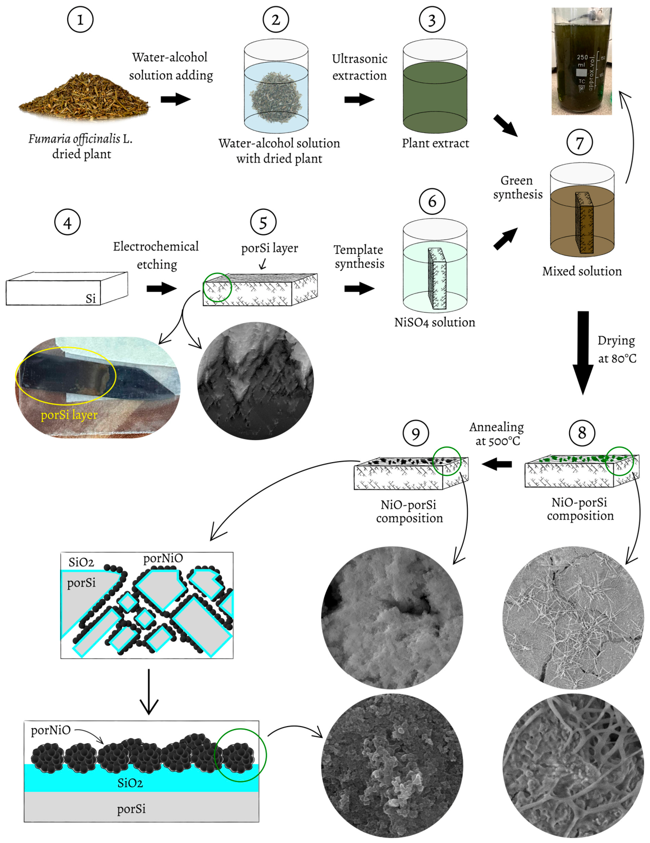
A detailed scheme for the synthesis of hierarchical porous nickel oxide nanoparticles via the green synthesis method is presented in reference [39]. The synthesis scheme for the composition is shown in Figure 2.
Hierarchical porous nickel oxide nanoparticles were obtained via a green synthesis method using a plant extract in the presence of a porous silicon substrate. An extract of the plant Fumaria officinalis L. (1) was used as a reducing agent for the nickel salt [40]. Solution (2), consisting of 50 mL of isopropyl alcohol and 50 mL of distilled water, was used to obtain the plant extract by ultrasonic extraction (3) of 25 g of dried plant. The extraction time was 30 min.
A monocrystalline silicon wafer (4) was etched to obtain porous silicon layers (5). A silicon wafer with a preformed porous layer was placed into a solution (6) of 15 mmol of nickel sulfate NiSO4 (LenReactiv JSC, Saint-Petersburg, Russia). The plant extract was then added to this solution, and the mixture was stirred for 30 min (7). Subsequently, a 2% NaOH (LenReactiv JSC, Saint-Petersburg, Russia) solution was added, and the mixture was stirred for another 30 min. After that, the solution was subjected to ultrasonic waves for 30 min. The porous silicon wafer with the deposited particles was dried in air at 80 °C (8). The wafer was then annealed at 500 °C (9). During the annealing process, the plant fibrils (8, SEM images) are burned out, thus forming larger pores within the structure (9, SEM images).
Furthermore, under these annealing conditions, oxidation of the porous silicon surface occurs [45], which promotes better attachment of particles to the pore surface and also isolates the porNiO nanoparticle layer from the silicon scaffold, thereby excluding the silicon scaffold from charge transport processes.
This technological sequence of synthesis and processing will enable the formation of a nanocomposition structure in which a coating of porous nickel oxide nanoparticles forms on the porous silicon surface (both external and internal, on the pore walls within the porous layer). This will create a complex three-dimensional hierarchical distribution of nickel oxide nanoparticles within a three-dimensional hierarchical porous silicon framework with a developed surface morphology. This hierarchical structure will ensure improved interaction with gas molecules via macropores for the rapid diffusion of gas particles, mesopores for a high degree of surface development, and increased surface area for increased interaction with gas particles.

2.3. X-Ray Diffraction Analisys

To study the nickel oxide phase composition, particles were taken from the surface of the obtained composition. The phase composition was studied by X-ray phase analysis using a powder X-ray diffractometer DRON-8N (Bourevestnik JSC, Saint-Petersburg, Russia). This instrument features a Mythen2 R 1K linear position-sensitive detector (Dectris Ltd., Baden, Switzerland) and a parabolic Goebel mirror. Powder X-ray diffraction was used with X-rays emitted from a Cu anode as the source of diffraction patterns. The X-rays were scanned at an angle of 10–70° two-theta with 0.01° step and an exposure time of 10 s.

2.4. NiO-porSi Composition Morphology and Elemental Composition

The surface morphology and porous structure of the NiO-porSi composition were characterized by scanning electron microscopy (SEM) using a TESCAN MIRA3 Electron Microscope (TESCAN, Brno, Czech Republic). The elemental composition of the samples was determined by X-ray spectral microanalysis using an EDS OXFORD Instruments X-MaxN80 detector (Oxford Instruments, High Wycombe, UK).
Transmission electron microscope (TEM) imaging was performed on a Hitachi HT7700 electron microscope (Hitachi High-Technologies Corp., Tokyo, Japan) with thermionic electron source optimized for material characterization at relatively low accelerating voltages up to 120 kV.

2.5. The BET Method for Studying the Specific Surface Area

The 4-point BET method was used to study the parameters of the resulting porous structure, such as the specific surface area [46].
The determination of the specific surface area is based on measuring the amount of adsorbate gas sorbed on the surface of the test sample at the temperature of liquid nitrogen and various relative partial pressures (P/P0) (P is the partial pressure of the adsorbate; P0 is the pressure of the saturated steam of the adsorbate at the temperature of liquid nitrogen T = −196 °C).
The specific surface area was studied using a Sorbi device (META CJSC, Novosibirsk, Russia). Prior to the study, the sample was subjected to thermal conditioning at a temperature of 150 °C for 45 min.

2.6. Impedance Spectroscopy Studies

To investigate the gas-sensing properties, electrodes were applied to the surface of the composition using a conductive paste.
The gas-sensing performance of the NiO-porSi nanocomposition was investigated by electrochemical impedance spectroscopy using a Z500P impedance analyzer (Elins Ltd., Chernogolovka, Russia). The frequency dependences of the complex resistance module and the phase shift angle between current and voltage in a capacitive circuit were measured in the frequency range from 100 Hz to 500 kHz. The gas-sensing properties were studied under exposure to isopropyl alcohol vapor at concentrations ranging from 500 to 4000 ppm. Variations in the concentration of the target gas were established by adjusting the ratio of air flows (pure air and air containing organic solvent vapor).
Impedance spectroscopy measurements were performed after surface saturation by holding the structure in isopropyl alcohol vapor. The impedance was represented on the complex plane as dependences of the real and imaginary components of the complex resistance. Measurements were carried out at two temperatures: room temperature (22 °C) and an elevated temperature (250 °C).
Equivalent circuit analysis was performed using the EIS Spectrym Analyser software (ver. 1.0).

3. Results and Discussion

3.1. The Structural Characterization of NiO

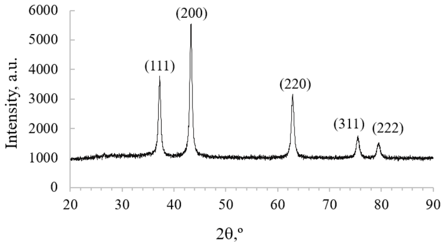
The XRD pattern of the NiO obtained using porSi template is shown in Figure 3.
XRD pattern shows the diffraction peaks of the (111), (200), (220), (311), and (222) crystal planes, corresponding to the face-centered-cubic (fcc) structure of the NiO.

3.2. NiO-porSi Composition Structure

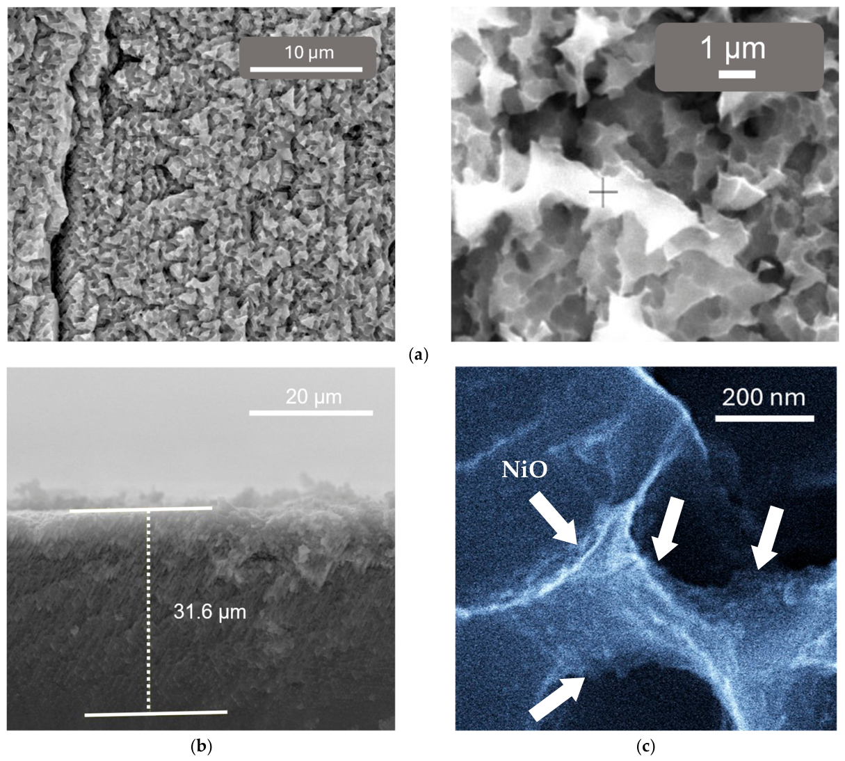
Figure 4a shows the wafer surface. Figure 4b shows a cross-section, where a branched pore channel system characteristic of Si (111) along the <100> family of directions can be seen, forming a (“fir tree”-like) dendritic-type porous texture. The thickness of the porous layer under these fabrication conditions for porous silicon was 31.6 μm. The porous structure consists of several types of pores. According to Figure 4a, the pore sizes on the surface are approximately 300–500 nm (macropores), while at a depth, they are 100–200 nm. Furthermore, SEM data reveal the presence of mesopores with a diameter of about 50–60 nm.
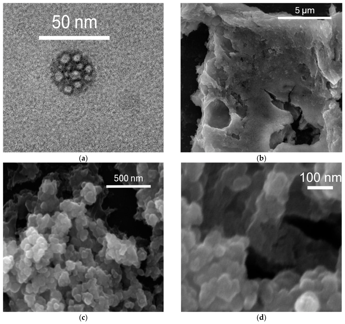
Figure 5 shows TEM and SEM images of porous hierarchical nickel oxide nanoparticles.
According to the TEM image in Figure 5a, the size of the nickel oxide nanoparticles is 3–5 nm. At the same time, in Figure 5b–d, it can be seen that the SEM results show the presence of larger agglomerates with a porous structure, measuring 30–50 nm. In reference [37], the results of porous characterization by sorption methods showed that nickel oxide particles obtained by this method possess a porous hierarchical structure, where larger particles with a diameter of 30–50 nm consist of nanoparticles measuring 3–5 nm. The detected pore diameters are 33 and 56 nm.
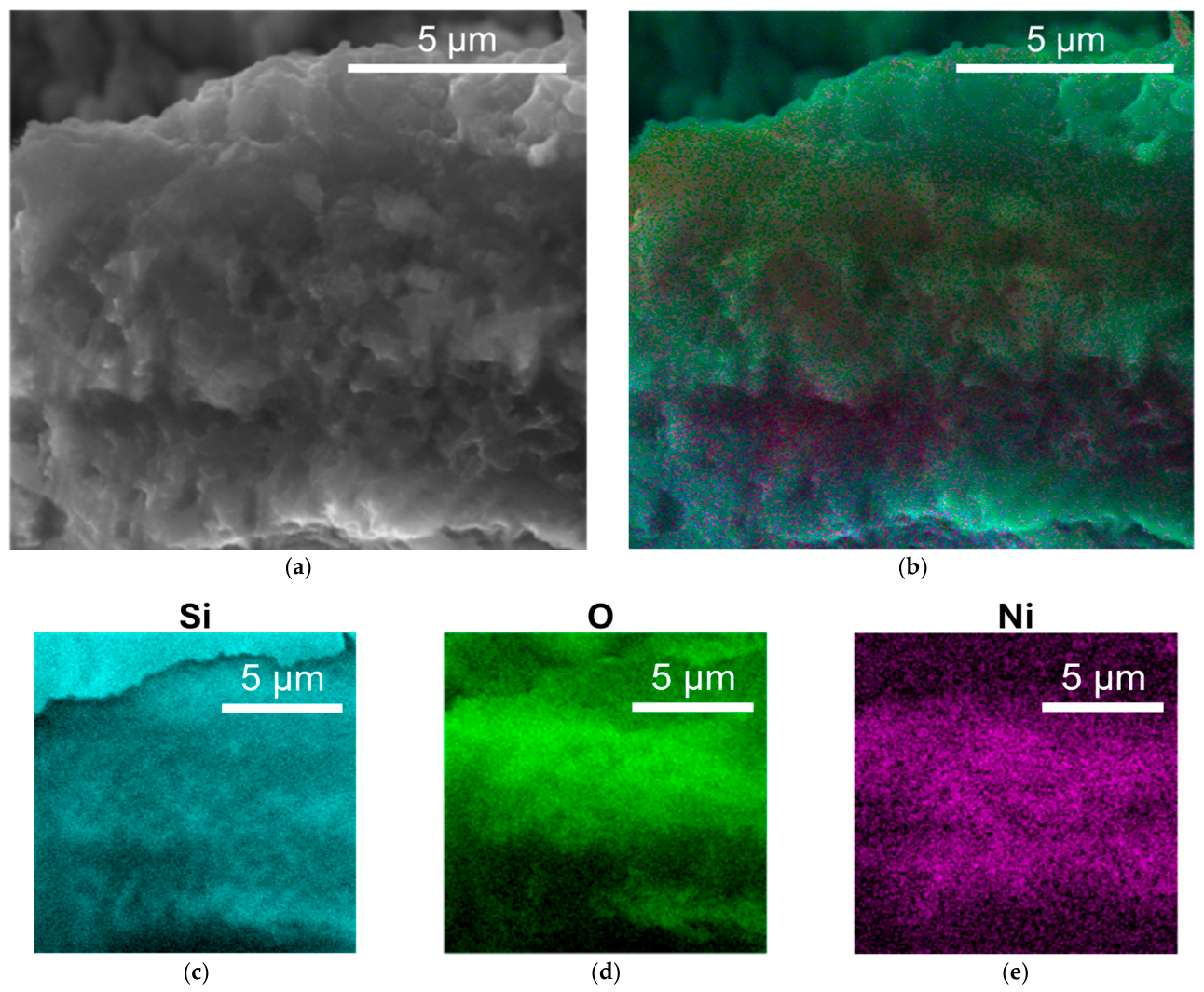
Figure 6a–e presents the results of the composition study by X-ray spectral microanalysis (EDS).
According to the Ni and O distribution maps in Figure 6d,e, oxygen and nickel are uniformly distributed throughout the porous silicon structure, indicating the formation of NiO nanoparticles. Throughout the synthesis, the silicon wafer was positioned in the container perpendicular to the liquid flow direction (as shown in Figure 2), which accounts for the formation of a larger volume of nickel oxide nanoparticles on one side of the porous silicon wafer.
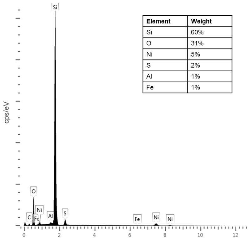
As can be seen from the Ni distribution maps in Figure 6b,d,e, nickel oxide formed not only on the surface of the porous silicon (Figure 6b, lower part of the wafer cross-section), but also inside the porous structure (Figure 6d,e). Figure 7 shows the EDS spectrum, in which the main elements, namely, Si, Ni, and O (silicon substrate, silicon oxide, nickel oxide nanoparticles), are detected. Also present are Al and Fe elements, which are likely residues from the tool used to prepare the wafer cross-section.
Thus, it has been demonstrated that synthesis in the presence of a porous silicon substrate with additional ultrasonic treatment allows for the formation of nickel oxide nanoparticles, achieves penetration of the material deep into the substrate pores, and enables the formation of such a 3D nanocomposition material based on hierarchical porous nickel oxide nanoparticles and silicon.

3.3. Investigation of Porous Structure

According to the results of the BET analysis of the composition structure, the specific surface area was 212.2 ± 2.3 m2/g for the NiO-porSi composition prepared using the green synthesis method for the preparation of nickel oxide nanoparticles and the template method for the preparation of the NiO-porSi composition.
As previously reported, the specific surface area of the nickel oxide nanoparticles obtained in this work is 130 m2/g. Thus, the obtained data demonstrate that the fabrication of a hybrid hierarchical porous structure based on nickel oxide nanoparticles and porous silicon makes it possible to obtain a structure with a surface area increased by almost a factor of 1.6.

3.4. Impedance Spectroscopy of NiO-porSi Composition

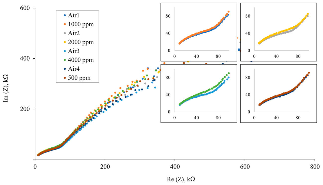
Figure 8 shows Nyquist plots for the NiO-porSi composition in air and in the presence of isopropanol vapor at a temperature of 22 °C.
The small difference between the impedances obtained at room temperature is due to the incomplete decomposition reaction of isopropyl alcohol vapor on the sample surface, since this process requires an elevated temperature; therefore, the reaction is weaker at room temperature.
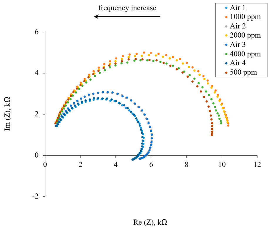
Figure 9 shows Nyquist plots for the NiO-porSi composition in air and in the presence of isopropanol vapor at a temperature of 250 °C.
From the obtained data, it can be seen that the resistance of the sample increases upon exposure to isopropyl alcohol vapor compared to its resistance in air.
In the measurements at room temperature, it can be observed that the change in resistance increases with increasing alcohol vapor concentration. This indicates incomplete saturation of the surface by isopropyl alcohol vapor due to the high specific surface area resulting from the contribution of the porous layer.
When measurements are carried out at an elevated temperature (250 °C), weak inductive behavior is observed in the low-frequency region. This fact indicates the fractal percolation nature of current flow at low frequencies in NiO-porSi systems involving NiO nanoparticles partially deposited on the surface and penetrating deep into the structure.
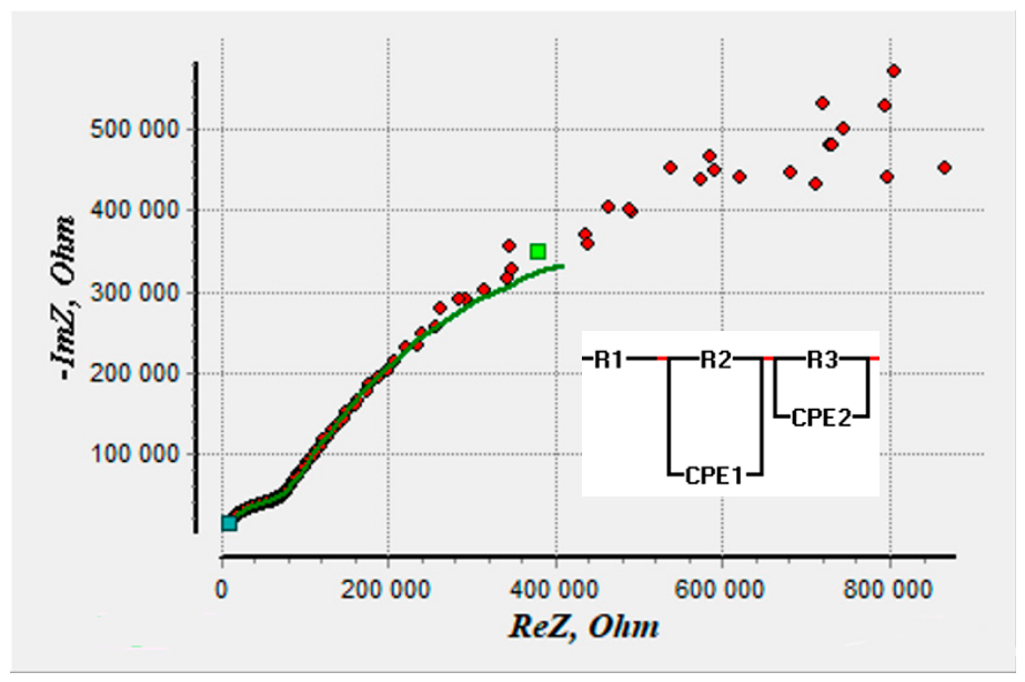
Figure 10 presents the results of equivalent circuit modeling for measurements performed at 22 °C. Since the difference between the impedance responses in air and in the presence of isopropyl alcohol vapor is small, the modeling for both cases is identical. Therefore, Figure 10 shows a common equivalent circuit for both conditions. The obtained equivalent circuit consists of two parallel R-CPE branches connected in series with an R element.
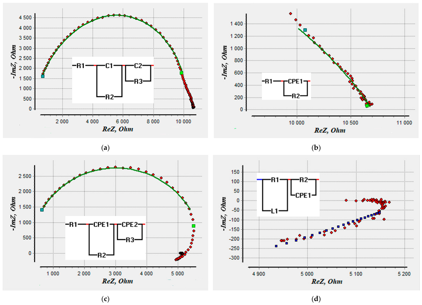
Figure 11 presents the results of equivalent circuit modeling for the impedance spectra at 250 °C in the presence of isopropyl alcohol vapor (Figure 11a,b) and in air (Figure 11c,d).
For the impedance in the presence of isopropyl alcohol vapor, the equivalent circuit (Figure 11a) consists of an R element connected in series with two R-C branches. For the low-frequency region (Figure 11b), a more accurate equivalent circuit is represented by an R element connected in series with a parallel R-CPE branch.
For the impedance in air (Figure 11c), the equivalent circuit consists of a resistance R connected in series with two parallel R-CPE branches. For the low-frequency region (Figure 11d), a more accurate circuit is represented by parallel R-L and R-CPE branches connected in series.
The analysis of the data with the construction of equivalent circuits (Figure 10 and Figure 11) revealed the presence of an inductive component in the low-frequency region when measuring the samples in an air atmosphere at 250 °C. The resulting equivalent circuit consists of two parallel R-L and R-CPE branches connected in series. The CPE (constant phase element), representing a non-ideal component, was used to more accurately describe the behavior of the observed dependences. Its parameter n, lying in the negative region, reflects the non-ideal inductive behavior of the system under study.
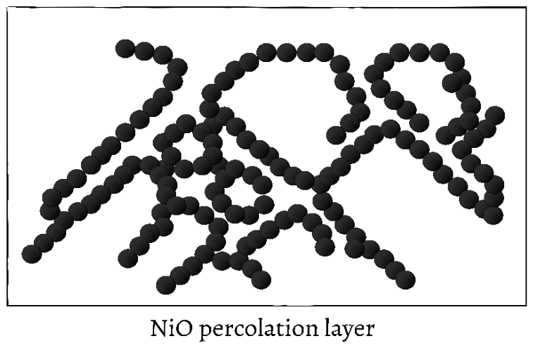
Moreover, upon interaction with the target gas molecules, not only the cross-section of the current flow channel changes, but also the path length of current flow. At low frequencies, the current flow trajectory may exhibit a tortuous (inductive) nature due to blocked regions, which disappear as the frequency increases. In reference [44], these features of current flow in fractal percolation networks (Figure 12) with a transition from inductive to capacitive behavior are explained on the basis of a simplified idealized model of the Mandelbrot–Given fractal. These features are expected to appear near the percolation threshold when it is slightly exceeded under conditions of target gas adsorption.
That the structure’s resistance is not dependent on gas concentration at an elevated temperature may be due to a high desorption rate, as a result of which an effective equilibrium between the processes of adsorption and decomposition of isopropyl alcohol vapor is not observed.

4. Conclusions

In this work, a technological approach has been proposed and implemented for the formation of a 3D nanocomposition material based on hierarchical porous nickel oxide nanoparticles incorporated into porous silicon. Porous silicon was used as a 3D porous template, in the presence of which the synthesis of porous hierarchical nickel oxide nanoparticles was carried out using a green synthesis method with a porous silicon substrate, followed by annealing in an oxygen-containing atmosphere.
SEM and TEM data showed that porous hierarchical nickel oxide particles are formed under the selected technological conditions. EDS analysis demonstrated that element distribution occurs throughout the entire depth of the porous layer. Thus, a composition with a multi-porous structure and a developed surface area is formed. In the composition, the thickness of the porous silicon layer is 31.6 μm, and the pore structure includes different types of pores: macropores with sizes of 300–500 nm on the surface and 100–200 nm at depth, as well as mesopores of 50–60 nm; the nickel oxide nanoparticles have sizes of 3–5 nm, subsequently assembling into particles with sizes of 30–50 nm and larger.
According to the BET analysis of the composition, the specific surface area was found to be 212.2 ± 2.3 m2/g, which corresponds to a 1.6-fold increase compared to the specific surface area of the initial nickel oxide nanoparticles.
Gas sensing tests performed in the presence of isopropanol vapor on these materials revealed weak inductive behavior in the low-frequency region at elevated temperatures. This fact indicates the fractal percolation nature of current flow at low frequencies in NiO-porSi systems involving NiO nanoparticles partially deposited on the surface and penetrating deep into the structure.
Thus, it has been shown that 3D nanocomposition structures based on hierarchical porous nickel oxide nanoparticles incorporated into porous silicon have potential for application as gas sensor materials.

Author Contributions

Conceptualization, K.K. and Y.M.S.; methodology, Y.M.S., A.A.B., D.A.K. and V.A.M.; experiment, K.K. and A.A.B.; resources, D.A.K.; writing—original draft preparation, K.K., Y.M.S. and A.A.B.; writing—review and editing, Y.M.S. and A.A.B.; visualization, K.K. All authors have read and agreed to the published version of the manuscript.

Funding

This research received no external funding.

Institutional Review Board Statement

Not applicable.

Informed Consent Statement

Not applicable.

Data Availability Statement

The original contributions presented in this study are included in the article. Further inquiries can be directed to the corresponding author.

Conflicts of Interest

Author Dmitriy A. Kozodaev was employed by the NT-MDT BV. The remaining authors declare that the research was conducted in the absence of any commercial or financial relationships that could be construed as a potential conflict of interest.

References

  1. Yang, Y.; Chen, L.-H.; Li, Y.; Rooke, J.C.; Sanchez, C.; Su, B.-L. Hierarchically porous materials: Synthesis strategies and structure design. Chem. Soc. Rev. 2017, 45, 481–558. [Google Scholar] [CrossRef] [Scilit]
  2. Maji, S.; Shrestha, L.K.; Ariga, K. Nanoarchitectonics for Hierarchical Fullerene Nanomaterials. Nanomaterials 2021, 11, 2146. [Google Scholar] [CrossRef] [Scilit] [PubMed]
  3. Jose, A.; Mathew, T.; Fernández-Navas, N.; Querebillo, C.J. Porous Inorganic Nanomaterials: Their Evolution towards Hierarchical Porous Nanostructures. Micro 2024, 4, 229–280. [Google Scholar] [CrossRef] [Scilit]
  4. Acharyya, R.N.; Bhadra, B.N.; Shahi, S.; Hayashida, K.; Fujita, S.; Takeyasu, K.; Ariga, K.; Shrestha, L.K. Nanoarchitectonics of Metal–Organic Framework on Fullerene Assemblies: Fabrication of Hierarchical Nanostructured Carbon Electrocatalysts. ACS Appl. Mater. Interfaces 2026, 18, 28717–28727. [Google Scholar] [CrossRef] [Scilit] [PubMed]
  5. Saber, S.; Rozali, S.; Haseeb, A. Synthesis of NiO-SnO2 cauliflower-like gas sensor material using a facile hydrothermal method for acetone detection. Mater. Res. Express 2024, 11, 106301. [Google Scholar] [CrossRef] [Scilit]
  6. Paruthi, A.; Sanjay, S.; Bhat, N. Functionalized Nanomaterials for Designing Nano/Micro Biologically Sensitive Field-Effect Transistors (Bio-FETs). In Functionalized Nanomaterials for Electronic and Optoelectronic Devices: Design, Fabrications and Applications; Wiley: New York, NY, USA, 2025; pp. 491–539. [Google Scholar] [CrossRef] [Scilit]
  7. Li, M.; Wu, C.; Wang, Z.; Wu, Z.; Huang, W.; Chen, J.; Yu, K.; Wen, T.; Yin, H.; Wang, Z. Enhanced Gas Classification in Electronic Nose Systems Using an SMOTE-Augmented Machine Learning Framework. Sensors 2026, 26, 714. [Google Scholar] [CrossRef] [Scilit] [PubMed]
  8. Chen, N.; Xiao, T.-H.; Luo, Z.; Kitahama, Y.; Hiramatsu, K.; Kishimoto, N.; Itoh, T.; Cheng, Z.; Goda, K. Porous Carbon Nanowire Array for Surface-Enhanced Raman Spectroscopy. Nat. Commun. 2020, 11, 4772. [Google Scholar] [CrossRef] [Scilit] [PubMed]
  9. Bobkov, A.; Luchinin, V.; Moshnikov, V.; Nalimova, S.; Spivak, Y. Impedance Spectroscopy of Hierarchical Porous Nanomaterials Based on por-Si, por-Si Incorporated by Ni and Metal Oxides for Gas Sensors. Sensors 2022, 22, 1530. [Google Scholar] [CrossRef] [Scilit] [PubMed]
  10. Bhadra, B.N.; Acharyya, R.N.; Shahi, S.; Ariga, K.; Shrestha, L.K. Metal–organic framework on fullerene (MOFOF) derived Co-anchored hierarchical carbon nanocomposite for catalytic nitroarene reduction. J. Mater. Chem. A 2026, 14, 19423–19431. [Google Scholar] [CrossRef] [Scilit]
  11. Asaldoust, F.; Mabhouti, K.; Jafari, A.; Taleb-Abbasi, M. Structural, magnetic, and optical characteristics of undoped and chromium, iron, cobalt, copper, and zinc doped nickel oxide nanopowders. Sci. Rep. 2025, 15, 1088. [Google Scholar] [CrossRef] [Scilit] [PubMed]
  12. Hotovy, I.; Huran, J.; Siciliano, P.; Capone, S.; Spiess, L.; Rehacek, V. Enhancement of H2 sensing properties of NiO-based thin films with a Pt surface modification. Sens. Actuators B Chem. 2004, 103, 300–311. [Google Scholar] [CrossRef] [Scilit]
  13. Kamal, B.; Suman, R.; Surajkumar, S.N. Review on NiO thin film as hole transport layer in perovskite solar cell. Nanosyst. Phys. Chem. Math. 2021, 12, 703–710. [Google Scholar] [CrossRef] [Scilit]
  14. Nandi, P.; Park, H.; Shin, S.; Lee, J.-W.; Kim, J.Y.; Ko, M.J.; Jung, H.S.; Park, N.-G.; Shin, H. NiO as hole transporting layer for inverted perovskite solar cells: A study of X-ray photoelectron spectroscopy. Adv. Mater. Interfaces 2024, 11, 2300751. [Google Scholar] [CrossRef] [Scilit]
  15. Liu, S.; Liu, R.; Chen, Y.; Ho, S.; Kim, J.H.; So, F. Nickel oxide hole injection/transport layers for efficient solution-processed organic light-emitting diodes. Chem. Mater. 2014, 26, 4528–4534. [Google Scholar] [CrossRef] [Scilit]
  16. He, L.; Liao, Z.-M.; Wu, H.-C.; Tian, X.-X.; Xu, D.-S.; Cross, G.L.W.; Duesberg, G.S.; Shvets, I.V.; Yu, D.-P. Memory and threshold resistance switching in Ni/NiO core–shell nanowires. Nano Lett. 2011, 11, 4601–4606. [Google Scholar] [CrossRef] [Scilit] [PubMed]
  17. Khairy, M.; El-Safty, S.A. Mesoporous NiO nanoarchitectures for electrochemical energy storage: Influence of size, porosity, and morphology. RSC Adv. 2013, 3, 23801–23809. [Google Scholar] [CrossRef] [Scilit]
  18. Kaur, N. Nickel oxide nanostructures for gas sensing: Recent advances, challenges, and future perspectives. ACS Sens. 2025, 10, 1641–1674. [Google Scholar] [CrossRef] [Scilit] [PubMed]
  19. Almaev, A.V.; Karipbayev, Z.T.; Kakimov, A.B.; Yakovlev, N.N.; Kukenov, O.I.; Korchemagin, A.O.; Akmetova-Abdik, G.A.; Kumarbekov, K.K.; Zhunusbekov, A.M.; Mochalov, L.A.; et al. High-Temperature Methane Sensors Based on ZnGa2O4:Er Ceramics for Combustion Monitoring. Technologies 2025, 13, 286. [Google Scholar] [CrossRef] [Scilit]
  20. Yuan, C.; Ma, J.; Zou, Y.; Li, G.; Xu, H.; Sysoev, V.V.; Cheng, X.; Deng, Y. Modeling Interfacial Interaction between Gas Molecules and Semiconductor Metal Oxides: A New View Angle on Gas Sensing. Adv. Sci. 2022, 9, 2203594. [Google Scholar] [CrossRef] [Scilit] [PubMed]
  21. Petrov, V.V.; Sysoev, V.V.; Starnikova, A.P.; Volkova, M.G.; Kalazhokov, Z.K.; Storozhenko, V.Y.; Khubezhov, S.A.; Bayan, E.M. Synthesis, Characterization and Gas Sensing Study of ZnO-SnO2 Nanocomposite Thin Films. Chemosensors 2021, 9, 124. [Google Scholar] [CrossRef] [Scilit]
  22. Nalimova, S.; Shomakhov, Z.; Bobkov, A.; Moshnikov, V. Sacrificial Doping as an Approach to Controlling the Energy Properties of Adsorption Sites in Gas-Sensitive ZnO Nanowires. Micro 2023, 3, 591–601. [Google Scholar] [CrossRef] [Scilit]
  23. Ben Arbia, M.; Comini, E. Growth processing and strategies: A way to improve the gas sensing performance of nickel oxide-based devices. Chemosensors 2024, 12, 45. [Google Scholar] [CrossRef] [Scilit]
  24. Danjumma, S.G.; Abubakar, Y.; Suleiman, S. Nickel oxide (NiO) devices and applications: A review. Int. J. Eng. Res. Technol. 2019, 8, 461–467. [Google Scholar] [CrossRef] [Scilit]
  25. Song, X.; Gao, L.; Mathur, S. Synthesis, characterization, and gas sensing properties of porous nickel oxide nanotubes. J. Phys. Chem. C 2011, 115, 21730–21735. [Google Scholar] [CrossRef] [Scilit]
  26. Abubakar, D.; Ahmed, N.M.; Mahmud, S.; Algadri, N.A. Properties of NiO nanostructured growth using thermal dry oxidation of nickel metal thin film for hydrogen gas sensing at room temperature. Mater. Res. Express 2017, 4, 075009. [Google Scholar] [CrossRef] [Scilit]
  27. Gagarina, A.Y.; Bogoslovskaya, L.S.; Khalugarova, K.; Bobkov, A.A.; Kondratyev, V.M.; Shumilo, M.V.; Spivak, Y.M.; Moshnikov, V.A. Impedance spectroscopy of hybrid structures based on nanostructured silicon impregnated with Au and NiO. Uchen. Zap. Fiz. Fak. Mosk. Univ. 2022, 4, 2241402. [Google Scholar]
  28. Liu, Y.; Li, X.; Li, X.; Shao, C.; Han, C.; Xin, J.; Lu, D.; Niu, L.; Tang, Y.; Liu, Y. Highly permeable WO3/CuWO4 heterostructure with 3D hierarchical porous structure for high-sensitive room-temperature visible-light driven gas sensor. Sens. Actuators B Chem. 2022, 365, 131926. [Google Scholar] [CrossRef] [Scilit]
  29. Li, B.; Liu, H.; Zeng, Q.; Dong, S.; Feng, W. Hierarchical porous NiO doped ZnO nanocomposite for formaldehyde gas sensor with high sensitivity, fast response/recovery and good selectivity. Surf. Interfaces 2023, 36, 102502. [Google Scholar] [CrossRef] [Scilit]
  30. Ensafi, A.A.; Ahmadi, N.; Rezaei, B. Nickel nanoparticles supported on porous silicon flour, application as a non-enzymatic electrochemical glucose sensor. Sens. Actuators B Chem. 2017, 239, 807–815. [Google Scholar] [CrossRef] [Scilit]
  31. Salih, E.Y.; Bashir, M.B.A.; Rajpar, A.H.; Badruddin, I.A.; Bahmanrokh, G. Rapid fabrication of NiO/porous Si film for ultra-violate photodetector: The effect of laser energy. Microelectron. Eng. 2022, 258, 111758. [Google Scholar] [CrossRef] [Scilit]
  32. Thamri, S.; Raouadi, M.H. Enhancement of NiO/Si solar cell by adding porous silicon and a silicon dioxide SiO2 carrier selective layer. Mater. Lett. 2024, 360, 136002. [Google Scholar] [CrossRef] [Scilit]
  33. Amdouni, S.; Rahmani, M.; Zaïbi, M.-A.; Oueslati, M. Enhancement of porous silicon photoluminescence by electroless deposition of nickel. J. Lumin. 2015, 157, 93–97. [Google Scholar] [CrossRef] [Scilit]
  34. Gowda, S.R.; Pushparaj, V.; Herle, S.; Girishkumar, G.; Gordon, J.G.; Gullapalli, H.; Zhan, X.; Ajayan, P.M.; Reddy, A.L.M. Three-dimensionally engineered porous silicon electrodes for Li ion batteries. Nano Lett. 2012, 12, 6060–6065. [Google Scholar] [CrossRef] [Scilit] [PubMed]
  35. Soboleva, E.; Geydt, P.; Zakharchuk, I.; Spivak, Y.; Moshnikov, V.; Lähderanta, E. Properties of porous silicon precipitated with nickel for gas sensors. Sens. Lett. 2018, 16, 672–676. [Google Scholar] [CrossRef] [Scilit]
  36. Khalugarova, K.; Spivak, Y.M.; Kozodaev, D.A.; Moshnikov, V.A.; Dombrovskaya, A.A.; Khrapova, E.K. Hierarchical Porous Nickel Oxide Nanoparticles with High Specific Surface Area by Green Synthesis. Micromachines 2026, 17, 156. [Google Scholar] [CrossRef] [Scilit] [PubMed]
  37. Khalugarova, K.; Spivak, Y.M.; Moshnikov, V.A. Formation of Hierarchical Porous Nickel Oxide Nanoparticles by Green Synthesis. J. Russ. Univ. Radioelectr. 2024, 27, 55–67. (In Russian) [Google Scholar] [CrossRef]
  38. Xue, H.; Huang, F.; He, X.; Yu, Z.; Zhang, T.; Zhu, G.; Xia, C. Hierarchical Porous CdS–Co3O4 Heterostructures for H2S Gas Sensing at Room Temperature. ACS Appl. Nano Mater. 2025, 8, 18434–18445. [Google Scholar] [CrossRef] [Scilit]
  39. Fu, Q.T.; Yu, H.X.; Yang, M.R.; Xu, Y.M.; Zhao, D.; Bai, X.J.; Wang, P.; Huo, L.H.; Zhang, W.Z.; Sui, L.L. In situ growth of Ag-loaded hierarchical NiO microspheres for enhanced H2S-sensing performance and the sensing mechanism. Appl. Surf. Sci. 2025, 685, 162033. [Google Scholar] [CrossRef] [Scilit]
  40. Granitzer, P.; Rumpf, K.; Ohta, T.; Koshida, N.; Poelt, P.; Reissner, M. Porous silicon/Ni composites of high coercivity due to magnetic field-assisted etching. Nanoscale Res. Lett. 2012, 7, 384. [Google Scholar] [CrossRef] [Scilit] [PubMed]
  41. Thamri, S.; Raouadi, M.H. Improved capacitance of NiO and nanoporous silicon electrodes for micro-supercapacitor application. J. Mater. Sci. Mater. Eng. 2025, 20, 1. [Google Scholar] [CrossRef] [Scilit]
  42. Zhang, K.; He, D.; Lu, J.; Zhang, Y.; Liu, J.; Cao, X.; Ai, X.; Luo, Y.; Zhang, S.; Chen, D. Sinter-resistant cathodes via vapor-phase precursor migration for stable high-temperature CO2 electrolysis. Appl. Surf. Sci. 2026, 736, 166835. [Google Scholar] [CrossRef] [Scilit]
  43. Ulrich, M.; Bunde, A.; Kohl, C.D. Percolation and gas sensitivity in nanocrystalline metal oxide films. Appl. Phys. Lett. 2024, 85, 242–244. [Google Scholar]
  44. Moshnikov, V.A.; Nalimova, S.S.; Seleznev, B.I. Gas-sensitive layers based on fractal-percolation structures. Semiconductors 2014, 48, 1499–1503. [Google Scholar] [CrossRef] [Scilit]
  45. Zoubir, N.H.; Vergnat, M.; Delatour, T.; Burneau, A.; De Donato, P.; Barrès, O. Natural oxidation of annealed chemically etched porous silicon. Thin Solid Films 1995, 255, 228–230. [Google Scholar] [CrossRef] [Scilit]
  46. Fagerlund, G. Determination of specific surface by the BET method. Matériaux Constr. 1973, 6, 239–245. [Google Scholar] [CrossRef] [Scilit]
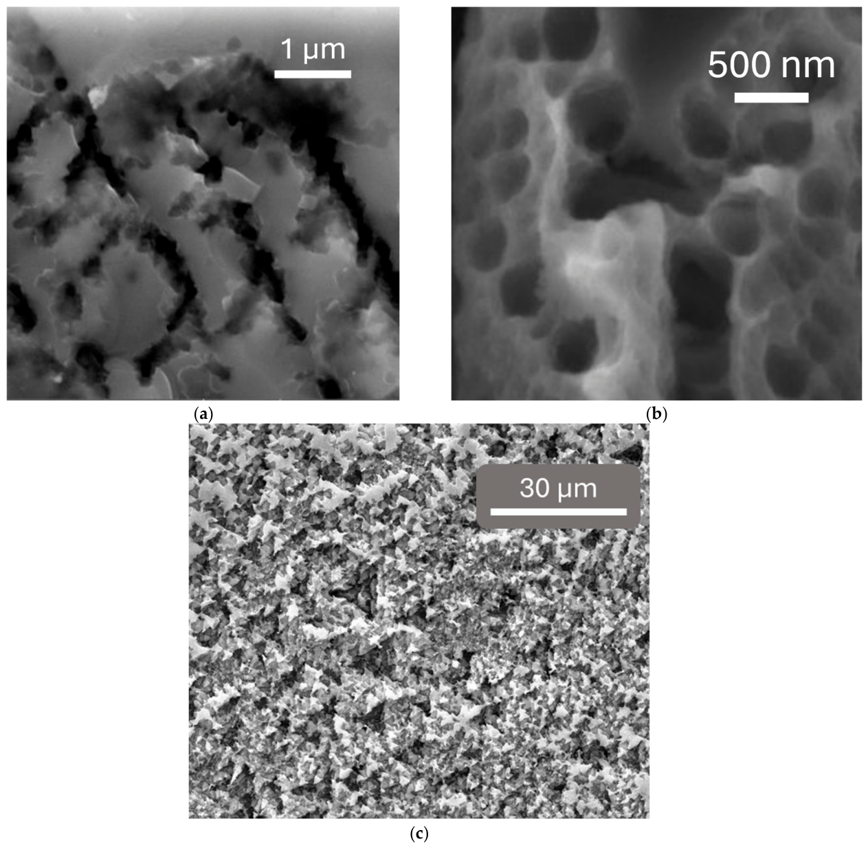
Figure 1. SEM images of the 3D porous silicon structure: (a) cross-section, side view; (b) 3D pore system; (c) surface, top view.
Surfaces 09 00071 g001
Figure 2. Synthesis scheme of the NiO-porSi composition.
Surfaces 09 00071 g002
Figure 3. XRD pattern of NiO nanoparticles obtained by using porSi template.
Surfaces 09 00071 g003
Figure 4. SEM images of a silicon wafer with a porous layer and synthesized porous nickel oxide nanoparticles: (a) wafer surface; (b) wafer cross-section; (c) porous nickel oxide particles on the porous silicon surface.
Surfaces 09 00071 g004
Figure 5. Morphology of obtained NiO porous nanoparticles: (a) TEM image; (b) SEM image, overview view, magnification 11.9k×; (c) SEM image, overview view, magnification 152k×; (d) SEM image, overview view, magnification 202k×.
Surfaces 09 00071 g005
Figure 6. EDS results of the composition study: (a) SEM image of a cross-section of the composition; (b) multi-layer elemental distribution map; (c) silicon distribution map; (d) oxygen distribution map; (e) nickel distribution map.
Surfaces 09 00071 g006
Figure 7. EDS data of the porNiO-porSi composition.
Surfaces 09 00071 g007
Figure 8. Dependence of the real part of impedance on the imaginary part for the NiO-porSi composition in air and in isopropanol vapor at room temperature (22 °C). The order of vapor concentration changes corresponds to the sequence indicated in the figure.
Surfaces 09 00071 g008
Figure 9. Dependence of the real part of impedance on the imaginary part for the NiO-porSi composition in air and in isopropanol vapor at an elevated temperature of 250 °C. The order of vapor concentration changes corresponds to the sequence indicated in the figure.
Surfaces 09 00071 g009
Figure 10. Nyquist diagram for sample at 22 °C in the presence of isopropanol vapor/air and simulated result with equivalent electrical circuit (red diamonds are experimental data, green and blue squares are the beginning and end of the simulation section, and the green line is the simulation line).
Surfaces 09 00071 g010
Figure 11. Nyquist diagrams for sample at 250 °C and simulated results with equivalent electrical circuits: (a) the whole diagram in the presence of isopropanol vapor; (b) the low-frequency region in the presence of isopropanol vapor; (c) the whole diagram in the air; (d) the low-frequency region in the air (red diamonds are experimental data, green and blue squares are the beginning and end of the simulation section, and the green line is the simulation line).
Surfaces 09 00071 g011
Figure 12. 2D-image of NiO percolation layer.
Surfaces 09 00071 g012
Disclaimer/Publisher’s Note: The statements, opinions and data contained in all publications are solely those of the individual author(s) and contributor(s) and not of MDPI and/or the editor(s). MDPI and/or the editor(s) disclaim responsibility for any injury to people or property resulting from any ideas, methods, instructions or products referred to in the content.