Article

Layered Structures Based on Ga2O3/GaS0.98Se0.02 for Gas Sensor Applications

1
Faculty of Physics and Engineering, Moldova State University, MD-2009 Chisinau, Moldova
2
National Center for Materials Study and Testing, Technical University of Moldova, MD-2004 Chisinau, Moldova
3
Academy of Sciences of Moldova, MD-2001 Chisinau, Moldova
*
Author to whom correspondence should be addressed.
Deceased author.
Surfaces 2025, 8(3), 53; https://doi.org/10.3390/surfaces8030053
Submission received: 9 May 2025 / Revised: 20 July 2025 / Accepted: 24 July 2025 / Published: 28 July 2025

Abstract

Efficient detection of toxic and flammable vapors remains a major technological challenge, especially for environmental and industrial applications. This paper reports on the fabrication technology and gas-sensing properties of nanostructured Ga2O3/GaS0.98Se0.02. The β-Ga2O3 nanowires/nanoribbons with inclusions of Ga2S3 and Ga2Se3 microcrystallites were obtained by thermal treatment of GaS0.98Se0.02 slabs in air enriched with water vapors. The microstructure, crystalline quality, and elemental composition of the obtained samples were investigated using electron microscopy, X-ray diffraction, and Raman spectroscopy. The obtained structures show promising results as active elements in gas sensor applications. Vapors of methanol (CH3OH), ethanol (C2H5OH), and acetone (CH3-CO-CH3) were successfully detected using the nanostructured samples. The electrical signal for gas detection was enhanced under UV light irradiation. The saturation time of the sensor depends on the intensity of the UV radiation beam.

1. Introduction

GaS0.98Se0.02 is an n-type lamellar semiconductor material in the GaSxSe1−x solid solution (SS) series. The crystals of these solid solutions have a hexagonal crystal lattice and energy bandgap that varies from 2.0 eV for x = 0 to 3.0 eV for the composition where x = 1 [1,2,3,4,5]. The SS with x = 0.02 represents a photosensitive material in the blue-violet region, with intense photoluminescence in the red region and optical transparency in a wide range of wavelengths from the visible region to ~20 µm [6]. The thermal treatment (TT) in air or in the atmosphere of an inert gas enriched with water vapors results in chemical transformations of GaS and GaSe compounds into monoclinic Ga2S3 and Ga2Se3 ones, with the additional formation of micro- and nano-structures (nanowires, nanoblades) of β-Ga2O3, which are promising for optoelectronics, gas sensors, and photocatalytic applications [7,8,9,10,11,12]. Being a direct bandgap material in a wide range of energies (4.4 to 5.0) eV [13,14], β-Ga2O3 oxide is considered an excellent material for photoreceptors in the UVC region (220 to 290) nm [15], while the nanoarchitectures based on it are promising for power electronics applications [16], for applications as photocatalytic electrodes, especially for the degradation of organic pollutants [17,18], and as gas sensors (H2, O2, CO, and other volatile organic compounds such as (CH3)2CO, C2H5OH, H2O, etc.) [19,20,21,22]. It was demonstrated by Girija et al. [23] that β-Ga2O3 nanorods show good antimicrobial activity. The electrical conductivity of β-Ga2O3 oxide at room temperature is determined by the concentration of electrons in the conduction band and their mobility, while the sensory properties of the β-Ga2O3 nanorods are influenced by the probability of formation of adsorbed reactive oxygen species (O and O2) on the surface and by their interaction mechanisms with gas molecules [24,25,26]. Since the dissociation energy of the O2 molecule is ~5.08 eV [27], at low temperatures as well as at room temperature, the probability of the formation of oxygen ions (O și O2−) at the surface of β-Ga2O3 is low. At room temperature, the ionized oxygen molecules form at the surface of the β-Ga2O3 nanowires, with their density being determined by the concentration of the adsorption/desorption centers [28]. Considering this, it is essential that the resistive gas sensors based on β-Ga2O3 are built on porous structures, including nanowires or nanometer-thin layers [29,30]. There are multiple technologies for obtaining β-Ga2O3 with different shapes (nanowires, nanobelts, nanorods, nanolamelas, etc.) [8,31,32,33]. Calestani et al. in [31] reports on the synthesis of β-Ga2O3 nanowires in a bi-zonal thermal reactor using Ar/N2 as transport gas. For this, metallic Gallium is heated at ~950 °C in the source zone, while the substrate zone, where the gallium oxide is obtained, is kept at a lower temperature, between 450–650 °C. Homogeneous layers of β-Ga2O3 nanowires and nanorods have been obtained through thermal oxidation of GaAs, GaS, and GaN powder at temperatures between 900 and 950 °C in a controlled atmosphere of Ar/N2 [8,32,33]. The GaS and GaSe crystals as well as their solid solutions (GaSxSe1−x, 0 ≤ x ≤ 1.0) are composed of planar packings of atoms in materials with a chalcogen layer on the surface. Since the valence bonds at the surface of the plates made of these materials are closed, the defects on the surface can serve as centers for initiation of Ga2O3 crystal growth. As the covalent radius of selenium is approximately 1.14 times larger than that of sulfur, the concentration of defects on the surface of the GaSxSe1−x (0 ≤ x ≤ 1.0) solid solution crystals and, respectively, the concentration of centers for the formation of β-Ga2O3 crystals can be sufficient for obtaining homogeneous layers of β-Ga2O3 nanowires. This process is also attributed to the diffusion of oxygen atoms through the cracks between the layered packings, the size of which is estimated to be approximately 0.33 nm [34].
Ga2O3 is characterized by a wide bandgap, making it ideal for deep-UV photodetectors, high-power electronics, and optoelectronic devices. Its exceptional thermal stability, up to about 1800 °C, enables its use in high-temperature and harsh environment applications. The material also boasts a high breakdown field strength, reaching as much as 8 MV/cm, supporting robust high-voltage power devices capable of handling higher switching voltages with improved power efficiency. Additionally, Ga2O3 exhibits high optical transparency (>80%) across visible and UV wavelengths, which is advantageous for UV detectors and transparent electronic devices. It exists in six polymorphic forms (α, β, γ, δ, ε, κ), with the β-phase being the most stable and widely employed in device fabrication due to its superior thermal and chemical stability; its monoclinic structure includes two types of gallium ions (tetrahedral and octahedral coordination) and oxygen ions, leading to anisotropic physical properties such as directional thermal conductivity, which can be up to 2.5 times higher along certain axes. The electrical conductivity of Ga2O3 is mainly governed by oxygen vacancies, which can be controlled during growth to produce either insulating or n-type semiconducting behavior, though p-type doping remains a significant challenge due to high activation energies of acceptors and the flat valence band. Its surfaces demonstrate low defect densities, and interfaces with materials like GaN show low trap states (~1010 cm−2·eV), favoring high-quality heterojunctions. Ga2O3 can be synthesized via diverse methods—including thermal oxidation, metal-organic chemical vapor deposition (MOCVD), pulsed laser deposition (PLD), mist-CVD, and molecular beam epitaxy (MBE)—with growth conditions greatly influencing film quality, phase stability, and defect levels. These favorable properties make Ga2O3 highly promising for applications such as high-voltage power devices, deep-UV photodetectors, gas sensors, transparent electronics, and as a gate insulator in GaN-based devices. Overall, Ga2O3’s combination of a wide energy bandgap, high breakdown field, thermal resilience, and optical transparency positions it as a versatile material for next-generation high-power, UV, and transparent electronic applications, with ongoing research focusing on overcoming challenges related to p-type doping and interface quality to fully realize its technological potential [35,36,37,38].
In this work, homogeneous layers of β-Ga2O3 nanostructures were obtained using thin monocrystalline layers of GaS0.98Se0.02 solid solutions. As mentioned above, one of the applied directions of nanostructured β-Ga2O3 oxide is its use in electroresistive gas sensors, functioning over a wide range of temperatures. The gas sensitivity of structures based on oxide semiconductors (In2O3, Ga2O3, ZnO, SnO2, etc.) is determined by the mechanism of generation and diffusion of oxygen vacancies in nano and microstructures. This phenomenon was first observed in ZnO and later termed the photogating effect in subsequent studies [39]. The effect is distinct from the regular photoconductive effect and is often observed in photodetectors based on low-dimensional materials and their heterostructures [40]. β-Ga2O3, as a wide bandgap semiconductor, has demonstrated high sensitivity to gases at temperatures from 450 to 1000 °C [28,41,42]. At temperatures within this range, oxygen vacancies contribute to the formation of molecular ions of O and O2− on the surface of the nanomaterial. At room temperature, the oxygen vacancies are bound in the crystalline network of the material, which leads to a low concentration of molecular oxygen ions and, consequently, to reduced sensitivity to gases and vapors of organic compounds. At the same time, the vapors of volatile organic compounds absorbed on the surface and in the morphological inhomogeneities of the nanowires contribute to the change in the dielectric permittivity of the material as a whole and, consequently, to the variation in the electrical capacitance of the capacitor based on this material [43]. In ref. [44,45], measurements of the differential electrical capacitance highlighted low concentrations of acetone. In addition, models for the bonding of organic molecules absorbed on the surface of β-Ga2O3 nanowires were proposed. Various ionized species from the vapors and gases absorbed on the surface of β-Ga2O3 nanowires have been obtained through ultraviolet (UV) radiation, a phase that can lead to increased gas sensitivity. The influence of UV radiation on the sensitivity of the electroresistive sensor made from β-Ga2O3 nanowires to water vapor was investigated in ref. [44]. According to the obtained results, at low concentrations of water vapor, UV radiation contributes to the formation of an excess of electrons and holes on the surface of the β-Ga2O3 nanowires, while at high concentrations of H2O vapor, the electrical conductivity is influenced by both the excess of electrons and holes as well as ionic molecules (OH).
This paper describes the technology of fabrication, properties, composition, surface morphology, and sensing performances to ethanol (C2H5OH), methanol (CH3OH), and acetone (CH3)2CO vapors of the layers consisting of β-Ga2O3 nanowires/nanoribbons with inclusions of Ga2S3 and Ga2Se3 microcrystallites on a substrate based on GaS0.98Se0.02 solid solution.

2. Materials and Methods

The nanostructured β-Ga2O3/GaS0.98Se0.02 was obtained by thermal treatment (TT) of the GaS0.98Se0.02 monocrystalline plates at 900 °C for 6 h in a humid atmosphere. The GaS0.98Se0.02 single crystals were grown by the Bridgman method in a tubular furnace with two temperature zones. The GaS0.98Se0.02 compound with a total mass of 20 g was synthesized from elemental Ga(5N), Se(5N), and S (spectrally pure), taken in stoichiometric amounts. Chemical elements were placed in a quartz tube of 200 mm length with an internal diameter of 14 mm. The inner side of the tube was coated with a thin layer of graphite. After venting the air to a pressure of ~1.5 × 10⁻⁵ Torr and sealing, the ampoule was placed in the first sector of the furnace and slowly heated until 1300 °C, at the rate of 70 °C per hour. The synthesis reaction at this temperature took 8 h.
During the synthesis, 1/4 of the length of the ampoule was kept outside the furnace and cooled by air flow. After the completion of the synthesis process, the tube slipped through the whole reactor, passing the temperature gradient 1300 °C/800 °C between sectors I and II of the furnace at a speed of ~1 mm/h. The material synthesized at the temperature of 800 °C was further cooled down to room temperature at the rate of ~100 °C/h.
The monocrystalline ingots were cleaved in ~230 to 900 µm thick plane-parallel slabs with smooth surfaces, which were optically transparent, without microscopic defects, and with a surface area of 5 × 8 mm2. In order to obtain the desired nanostructures, the GaS0.98Se0.02 samples were annealed at 900 °C in air for a time interval from 30 min to 6 h. As a result, the surface of the slabs proved to be covered with a white microstructured layer of β-Ga2O3. Using thermal evaporation in vacuum (10−5 Torr), two strips (thickness of 400 nm) of Indium were deposited on each side, keeping the distance between them to about 2 mm. Further, in order to obtain In2O3 electrodes, the samples were subjected to thermal treatment at 900 °C for 30 min in air. The In/In2O3 layers on the surface of the sample served as electrodes for electrical conductivity measurements during the gas sensing experiments. The optical absorption edge in thin structures of In2O3 varies from 3.66 eV [45] to 4.09 eV [46].
The microstructure, crystal quality, and elemental composition of the β-Ga2O3 layer formed on the surface of the GaS0.98Se0.02 slab was studied by SEM, X-ray diffraction, EDXS, and Raman spectroscopy. X-ray diffraction patterns with wavelength λCuKα = 1.54060 Å were measured using the Seifert 3000 TT diffractometer (40 kV and 40 mA) in the range of 2θ angles from 30° to 90°. The surface morphology of the β-Ga2O3 layer formed on GaS0.98Se0.02 was analyzed using a scanning electron microscope Vega TS 5130, Brno, Czech Republic (7 kV, 8 µA). The elemental composition of the surface of the β-Ga2O3 layer was determined by the EDX Spectroscopy method in the SEM microscope. The chemical composition of the primary material (GaS0.98Se0.02) and of the β-Ga2O3 layer on its surface was studied using the Raman spectra recorded with a Micro-Raman spectrometer (WITec Alpha-300 Ra, Oxford Instruments, Abingdon, UK) upon excitation with a 532 nm laser line. Diffuse reflectance spectra in the UVC region were recorded using a set-up based on an MDR-2 monochromator equipped with a 1200 mm−1 diffraction grating. The UVC radiation in the range from 220 nm to 280 nm was obtained by using a 1000 W Argon arc lamp, OSRAM, Germany, whose radiation passed through a monochromator with a quartz prism.

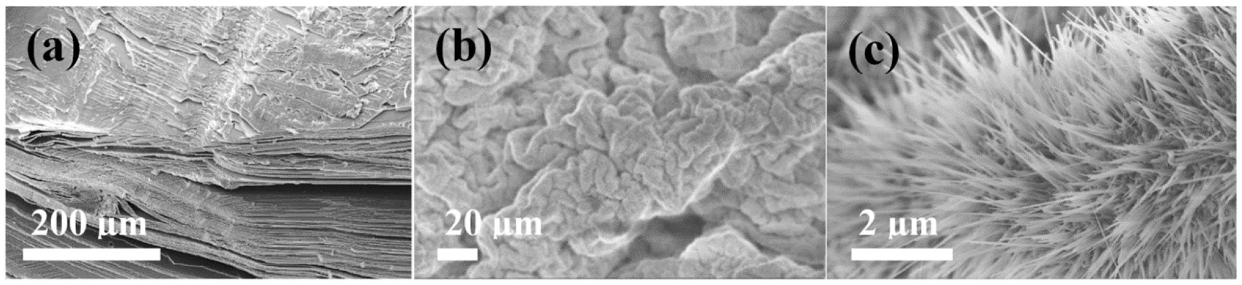
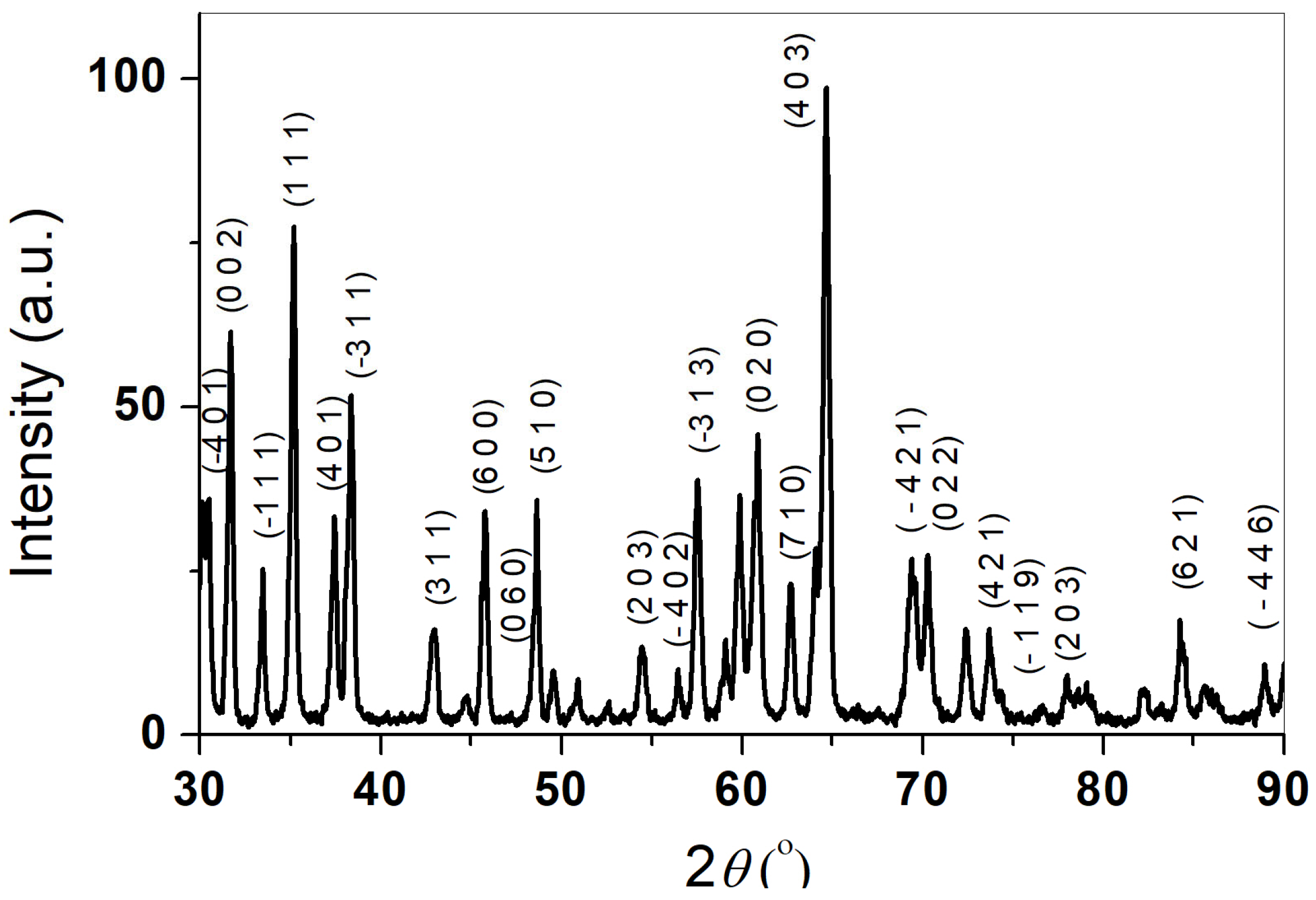
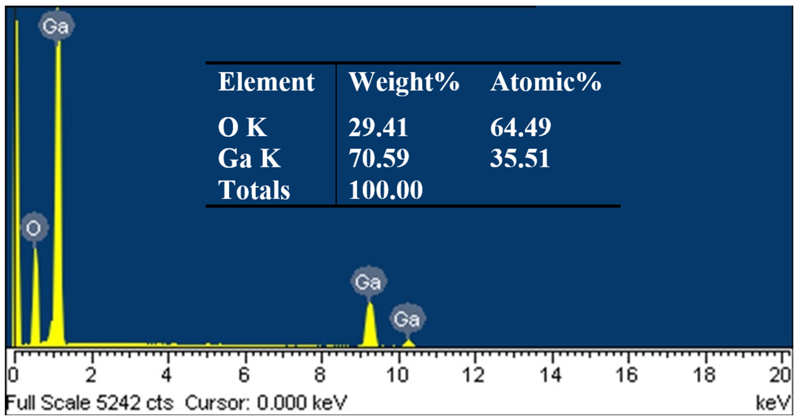
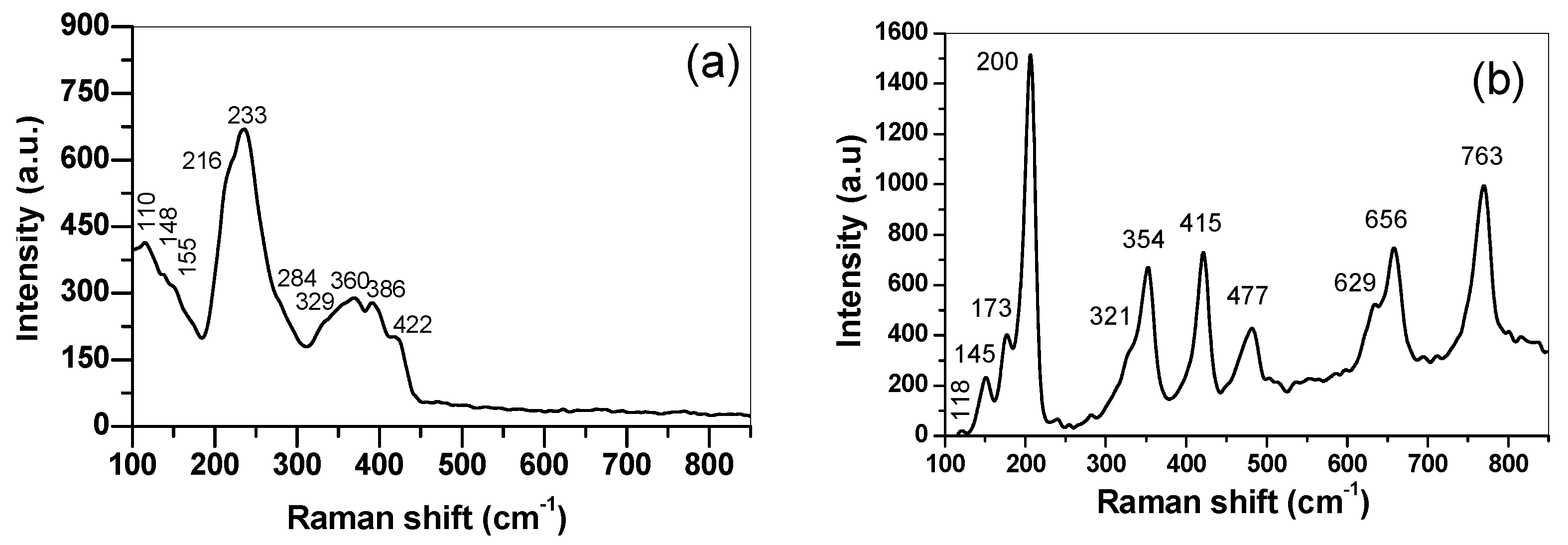
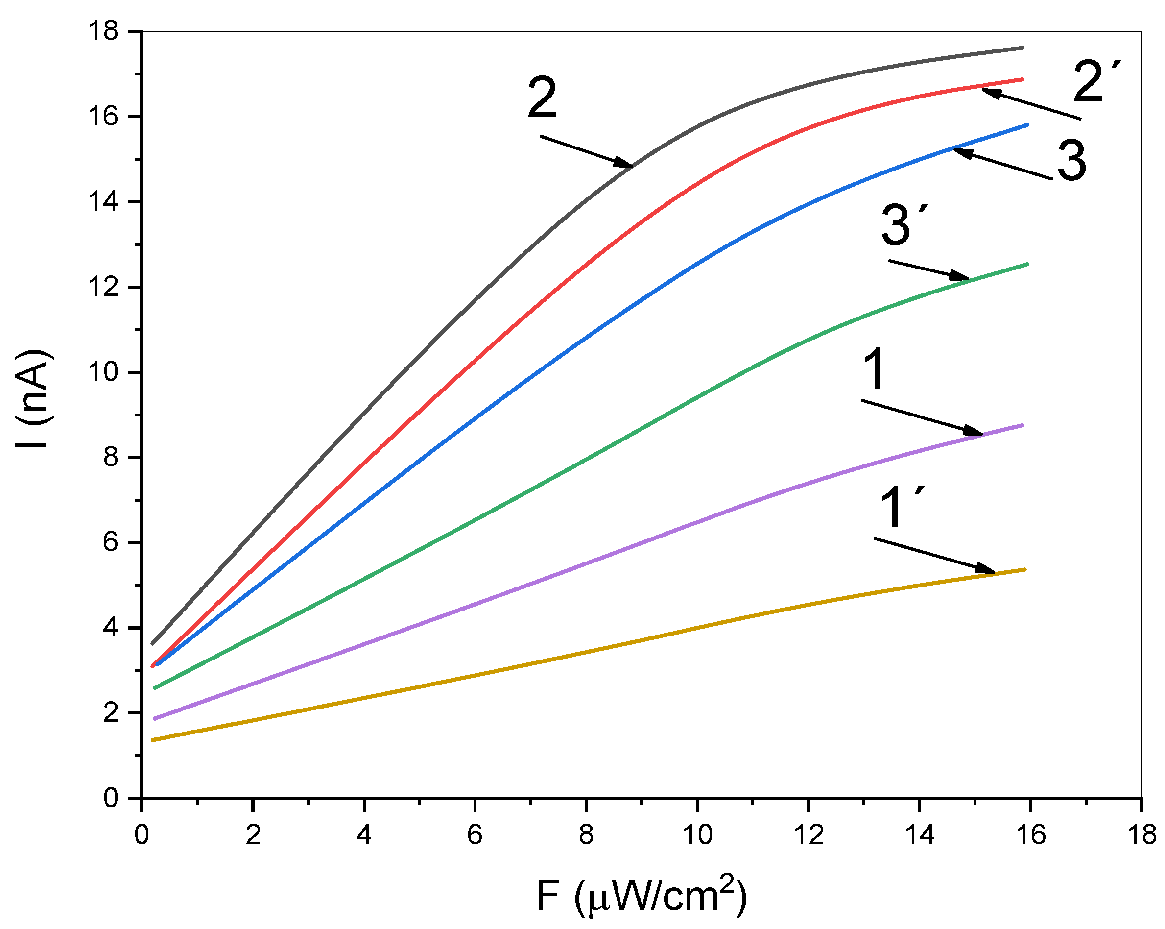
3. Results and Discussion

The formation of thin plates with smooth plane-parallel surfaces is characteristic for the crystals based on GaS and GaSe compounds. The valence bonds at the surface of the GaS/GaSe lamellae are closed, which leads to low concentration of surface states (~1010 cm−2) [47]. Atoms of the uncontrollable impurities or small amounts of specially implemented atoms are preferentially located in the space between the S/Se-Ga-Ga-S/Se packings, forming bridges between them and thus leading to an increase in the density of surface states on the cleaved surfaces of the respective single crystals. The surface states on the GaS/GaSe lamellae serve as nucleation centers of β-Ga2O3 nanostructures that form at high temperatures in the oxygen atmosphere. The high density of condensation centers on the edges of GaS/GaSe wafers stimulates the formation of gallium oxides. In the work presented in [48], the oxidation process of thin GaSe layers is studied, from which it can be seen that their oxidation is initiated at the edges of the GaSe sheets. To stimulate the formation of a homogeneous layer of β-Ga2O3 oxide, in this study we used GaS0.98Se0.02 plates. The SEM image in Figure 1a shows the structure of the GaS0.98Se0.02 plates used as initial material to obtain gas sensors based on β-Ga2O3 oxide.
The formation of such a structure of the oxide layer can be attributed to the distribution of oxide-forming germs and the contraction of the surface in monoclinic plates of GaS0.98Se0.02 by the replacement of sulfur ion (S2−), whose radius is 1.90 Å, with oxygen, whose ionic radius equals 1.46 Å (Figure 1b). The β-Ga2O3 nanoneedles, as seen in Figure 1c, are oriented in the direction perpendicular to the plate surface. Considering the length of nanoneedles, the average thickness of the Ga2O3 layer is ~5 µm.
The phase composition and crystallographic structure of the material obtained by TT in water vapor atmosphere at ~900 °C for 6 h was analyzed using the X-ray diffraction method (Figure 2).
As can be seen from Figure 2, the XRD reflections have a well-defined narrow contour characteristic of homogeneous and perfect crystallites.
The intense lines corresponding to the 2θ diffraction angles of X-rays with the wavelength λCuKα = 1.54060 Å equal 30.48°, 31.37°, 35.18°, 38.35°, 45.80°, 48.60°, 57.62°, 60.90°, 64.65°, 70.32°, and 84.42°. According to the PDF card No. 43-1012, these peaks are identified as reflection from sets of crystallographic planes with Miller indices (−4 0 1), (0 0 2), (1 1 1), (−3 1 1), 6 0 0), (5 1 0), (−3 1 3), (0 2 0), (4 0 3), (0 2 2), and (6 2 1) of the monoclinic c2/m space group of β-Ga2O3 with the lattice parameters a = 13.23 Å, b = 3.04 Å, c = 5.800 Å, and β = 103.7°. The reflections corresponding to 2θ angles equal to 49.15°, 53.60°, and 75.40°, according to the PDF card No. 760752, are identified as X-ray diffraction from crystallographic plane assemblies with the Miller indices (−3 3 0), (0 2 3), and (2 0 4) of the monoclinic Cc space group of α-Ga2S3 with crystallographic cell parameters a = 11.14 Å, b = 6.411 Å, c = 7.038 Å, and β = 121.23°. Along with the intense XRD lines corresponding to the diffraction from the monoclinic β-Ga2O3 and α-Ga2S3 crystallites at 2θ angles equal to 47.18°, a low intensity line is highlighted which, according to the PDF card No. 760 752, is attributed to the diffraction from the β-Ga2Se3 crystallite lattice. These lines are clearly highlighted in the XRD diagram of the thin Ga2Se3 layers obtained by the CVD method in the work [49].
Two stripes of In, 2 mm in width and ~400 nm thick, were deposited on the lateral surfaces of the slabs covered with β-Ga2O3 nanostructures.
The average dimensions “d” of the β-Ga2O3, α-Ga2S3, and Ga2Se3 crystals in the composite were determined from the analysis of the contours of the XRD lines with a wavelength of λ = 1.54060 Å using the Debye-Scherrer formula:
d   =   k λ β cos θ h k l
where k is the Scherrer constant equal to 0.94, λ is the wavelength of X-rays, θhkl is the Bragg diffraction angle, and β is the width of the diffraction line at half maximum intensity of the XRD line.
The dimensions of the β-Ga2O3 and α-Ga2S3 crystallites in the composite equal 27 nm and 18 nm, respectively, which were determined from the analysis of the contour of the X-ray diffraction lines corresponding to the 2θ angles equal to 35.18°, half-width of 20′, and 49.15°, half-width of 32′, respectively.
In [8], the phase transformations of GaS crystals obtained by the CVD method in the Ar atmosphere were studied. The TT at 700 °C of the GaS plate resulted in the formation of GaS, Ga2S3, and β-Ga2O3 crystallites, while the TT at the temperature of 900 °C showed the formation of a homogeneous material of β-Ga2O3 nanostructures with small amounts of α-Ga2S3 microcrystallites with a monoclinic crystal lattice.
The elemental chemical composition of the β-Ga2O3 layer formed by TT of the GaS0.98Se0.02 slab at 900 °C in a water vapor atmosphere was derived from the EDXS spectrum (EHT −5kV) (Figure 3). The thickness of the layer analyzed by EDXS can be approximated by the depth “l” of penetration into the material of electrons accelerated at 5 kV. This parameter can be determined using the Kanaya-Okayama formula [50]:
l = 0.0276 ρ A Z 0.89 E 0 n   ( µ m )
where A is the atomic weight (g/mol), E0 is the electron energy (keV), Z is the atomic number, ρ is the density (g/cm3); for E0 ≤ 5 keV, n = 1.35. Since the A and Z parameters of oxygen atoms have smaller values than those of Ga atoms, in the approximation of the l parameter, we will take AGa = 69.72, ZGa = 31, and ρ = 5.863 g/cm3 [51]. For these values of the parameters E0, n, A, and ρ, we obtain a thickness of 1.36 µm for the analyzed layer.
As seen from Figure 3, the investigated layer contains ~64.5% of O atoms and 35.5% Ga atoms. If one admits that the layer of material penetrated by the 5 keV electron beam represents the β-Ga2O3 compound, then this layer contains a surplus of ~11% of atomic oxygen (Figure 3). The absence of sulfur (S) and selenium (Se) peaks in the EDX spectrum (Figure 3) may be attributed to the selective surface oxidation process occurring at 900 °C in the humid atmosphere, where S and Se species are likely to evaporate or diffuse away due to their higher vapor pressures. Additionally, considering the EDX analyzed layer’s calculated thickness of approximately 1.36 µm and the Ga2O3 nanoneedles’ length of about 5 µm, the analysis might not penetrate deeply enough to detect the residual S and Se atoms. The complete transformation of the surface into a homogeneous oxide layer and possible out-diffusion of chalcogenides during annealing could explain the lack of detectable EDX signal from these elements.
The XRD patterns in the range of 2θ angles from 30° to 90° show the diffraction lines that can be attributed to several chemical compounds. According to PDF card No. 71009, No. 43 1017 and No.300577, the intense line at the angle 2θ = 33.409° can be attributed to the X-ray diffraction from the assemblies of planes with Miller indices (103) in β-Ga2O3 crystals, as well as (−402) in α-Ga2O3 and (−111) in β-Ga2O3 crystals. To identify the chemical composition of the thin layer of material formed on the surface of the GaS0.98Se0.02 plates by TT at a temperature of 900 °C in water vapor atmosphere we recorded the micro-Raman spectra.
Figure 4a shows a fragment of the Raman spectrum of the material obtained by TT at 900 °C for 30 min in the water vapor atmosphere of a monocrystalline plate of GaSxSe1−x with x = 0.98. Peaks with weak intensity are characteristic of structurally inhomogeneous strongly deformed crystallites [52]. The features (plateaus, peaks) with the wave numbers 110 cm−1, 148 cm−1, 233 cm−1, 329 cm−1, 386 cm−1, and 422 cm−1 (Figure 4a) are identified as vibrational modes related to the Wurtzite α-Ga2S3 crystal lattice [53,54].
In the range of wave numbers from 100 cm−1 to 450 cm−1, along with intense Raman lines of the monoclinic β-Ga2O3 lattice at wavenumbers 114 cm−1, 147 cm−1, 199 cm−1, and 346 cm−1 [55], there is a series of intense Raman lines related to Ga2S3 crystals at the wave numbers of 114 cm−1, 147 cm−1, 233 cm−1, and 386 cm−1 [53], as well as to Ga2Se3 at the wavenumbers 105 cm−1, 119 cm−1, 155 cm−1, 220 cm−1, 252 cm−1, and 283 cm−1 [56]. The Raman spectrum (Figure 4) in the range from 100 to 200 cm−1 can be seen as a result of merging the contours of the Raman bands with maxima centered at the wave numbers 114 cm−1 and 197 cm−1 of the β-Ga2O3 monoclinic lattice, as well as the peaks with maxima at 114 cm−1 and 147 cm−1 of the α-Ga2S3 monoclinic lattice. Also, the intense Raman band with the maximum at 233 cm−1 may be considered as superimposing the vibration bands of the Ga2Se3 crystallite network with maxima at 220 cm−1, 227 cm−1, and 254 cm−1 and the TO phonon band with the maximum at 233 cm−1 of the lattice vibration of α-Ga2S3 crystallites in the composite.
When increasing the TT duration from 30 min to 6 h, the Raman spectrum changes substantially (Figure 4b). In the wavenumber range from 100 cm−1 to 850 cm−1, 11 peaks with maxima centered at 116, 145.5, 173, 200, 321.7, 354, 415.2, 477, 629.5, 656, and 763 cm−1 are well defined [55]. The Raman spectra of the β-Ga2O3 single crystals and nanostructures (nanowires, nanoribbons) are well studied and presented in multiple works [57,58,59,60]. From the analysis of the previous results, a good correlation is found between the frequency of the vibration modes of the β-Ga2O3 lattice, regardless of the form (crystal, powder, nanostructure) and the method of obtaining the material.
So, one can conclude that during the first stage of oxidation of monocrystalline GaS0.98Se0.02 plates at 900 °C in atmosphere with water vapor, phase transformations occur with the formation of the α-Ga2S3 phase, after which, in the second stage of compositional transformation, the compound β-Ga2O3 is obtained in the form of nanowires. The process of formation of the nanostructured layer of β-Ga2O3 by oxidation of GaS/GaSe single crystals is described in the previous works [9,61] with the following relations:
3 ( G a S / G a S e ) + 3 2 H 2 O + 3 4 O 2 900   ° C G a ( O H ) 3 + 2 ( G a S / G a S e ) + S / S e
2 G a ( O H ) 3 900   ° C G a 2 O 3 + 3 H 2 O
12 ( G a S / G a S e ) + 3 O 2 900   ° C 4 G a 2 S 3 + 2 G a 2 O 3
2 G a 2 S 3 + 3 O 2 900   ° C 2 G a 2 O 3 + 6 S / S e
The methanol (CH3OH), ethanol (C2H5OH), and acetone (CH3-CO-CH3) vapor sensor was made of a β-Ga2O3 plate with a thickness of 0.3 mm and a surface area of 5 × 5 mm2, which was obtained by TT in air enriched with water vapor at 900 °C for ~6 h of a GaS0.98Se0.02 single-crystal plate.
Next, the sample was subjected to TT in air at 900 °C for one hour. As demonstrated previously [62,63], a thin layer of In subjected to rapid TT in atmosphere or N2 flow for one hour fulfils the function of an ohmic electrode (perfectly linear I-U characteristic) on n-type β-Ga2O3. The current through the sample in normal atmosphere at the electrode voltage of 30 V was 2.0 × 10⁻¹⁰ A. So, this material can be considered as a dielectric. The sample was placed in an optically transparent quartz tube closed at one end, into which the vaporizing agent was introduced in relevant quantities, so that saturated vapor formed in the tube at the temperature of 25 °C. Note that the control sample consisting of β-GaS plate was placed in the same tube.
Measurements of the sample response to methanol, ethanol, and acetone vapors were performed in alternating current mode. The experimental setup consists of an alternating current generator (100 kHz, 30 V) that is connected to the sample in series with a 10 kΩ resistor. The voltage drop across this resistor is amplified/measured with a selective voltmeter adjusted to a frequency of 100 kHz, so that the average current through the sample is obtained.
The dependence of the current intensity through the sample was recorded. Figure 5a shows the time dynamic curves of the increase in currents through the sensors in the presence of CH3OH, C2H5OH, and CH3-CO-CH3 vapors in the absence of UVC radiation, while Figure 5b presents the same measurements under 250 nm irradiation with a flux density of 12 µW/cm2.
As can be seen from Figure 5a, the current reaches the saturation state in ~260 s when exposed to CH3-CO-CH3 vapors, ~330 s for CHOH3, and ~220 s for C2H5OH. The intensity of the saturation current for CH3OH and C2H5OH vapors is ~3.5 to 3.6 nA, while for the acetone vapors it is ~2.0 nA. When exposed to the ambient atmosphere in the dark, oxygen is adsorbed on the surface of gallium oxide nanowires. In this process, electrons are removed from the conduction band, creating depletion layers in the near-surface region, which results in upward band bending and increased electrical resistance. When reducing gases of methanol, ethanol, or acetone are injected, they interact with chemisorbed oxygen ions, releasing electrons to the conduction band and thus leading to a decrease of electrical resistance, as was previously demonstrated by Yatskiv et al. using the XPS technique [64]. Under UV irradiation, the increased number of photogenerated electron–hole pairs leads to activation of the surface of β-Ga2O3 nanowires, that is, a direct band gap semiconductor of 4.8 to 5.0 eV [65,66]. Under UV light irradiation, the sensitivity of the β-Ga2O3 nanowire sensor improves (Figure 5b). The general mechanism of sensitivity improvement in the presence of UV might be explained considering the interaction of the used gases with the increased number of the adsorbed reactive species of oxygen on the sensor surface, which leads to a modification of the potential barrier and an increase in conductivity [67]. It is known that thin layers of β-Ga2O3 nanowires represent the photosensitive element of UVC radiation receptors [68,69]. Figure 5b shows the temporal dependence of the photoresponse dynamics of the sensor through the receptor circuit of β-Ga2O3 nanowires in the presence of CH3OH, C2H5OH, and CH3-CO-CH3 vapors. The photoresponse was determined from the following formula:
ρ = ( I U V I 0 ) I 0
where IUV is the current intensity through the sensor at the applied voltage of 30 V in the presence of vapors upon irradiation with UV radiation, and I0 is the current intensity in the absence of UV irradiation.
The 250 nm flux of UV radiation with the density of 12 µW/cm2 was selected from the emission spectrum of a 1000 W Xe vapor arc lamp using a quartz prism monochromator. The intensity of the UV radiation beam was determined with a calibrated Si photodetector. As can be seen from Figure 5b, a saturation photoresponse is reached in ~150 s in the presence of CH3-CO-CH3 vapor and ~180 s for CH3OH and C2H5OH vapors.
Figure 6 shows the dependences of the photoresponse through β-Ga2O3 photoresistors on the incident energy flux density from 0 to 16 µW/cm2 in the presence of saturated vapors of CH3-CO-CH3, C2H5OH, and CH3(OH).
As can be seen from this presentation, the photoresponse through the sample tends to saturate at an incident radiation density of 16 µW/cm2 for CH3-CO-CH3 vapors, more pronounced than for C2H5OH vapors. The ratio of the current density after 200 s excitation with 16 µW/cm2 of the sensor based on β-Ga2O3(GaS0.98Se0.02) nanowires to the β-Ga2O3(β-GaS) sensor is 1.05, 1.24, and 1.63 for CH3-CO-CH3, C2H5OH, and CH3(OH) vapors, respectively.
The development of β-Ga2O3/GaS0.98Se0.02 composites represents a promising advancement in gas sensor technology, particularly for environmental monitoring. Their enhanced sensitivity to volatile organic compounds like methanol, ethanol, and acetone makes them suitable for industrial applications where monitoring these vapors is crucial for safety and compliance. The ability to boost performance under UV light further broadens their applicability, allowing for more precise and responsive detection mechanisms in dynamic environmental conditions.
Future research could focus on integrating the sensors into portable and self-sufficient devices that incorporate alternative energy-efficient UV sources. Additionally, exploring catalyst additives or surface modifications might reduce the dependency on UV light, enhancing the sensors’ performance under ambient conditions. Further investigation into lowering the production temperature and optimizing the layer composition could streamline the fabrication process. Finally, testing the sensors in diverse environmental conditions would provide a broader evaluation of their robustness and functionality in real-world settings.

4. Conclusions

This study expands the range of materials suitable for developing sensors for environmental monitoring. By subjecting GaSxSe1−x solid solution slabs (x = 0.98) to thermal treatment at 900 °C in a humid atmosphere, a layer of β-Ga2O3 nanowires with Ga2S3 and Ga2Se3 microcrystallites is produced. These structures effectively detect methanol, ethanol, and acetone vapors, with sensitivity notably enhanced under UV light. The sensor’s saturation time ranges from 200 to 300 s, depending on UV radiation intensity. The photoresponse increases significantly, by 7.5 times with CH3-CO-CH3 vapors and ~15 times with CH3OH and C2H5OH vapors. This improvement can be attributed to the formation of reactive oxygen species amplified by UV-induced photoresponse. SEM, XRD, and Raman spectroscopy analyses provide insights into the material’s crystallographic and compositional changes, confirming its stability and suitability for sensor applications. These findings highlight the promising potential of β-Ga2O3/GaS0.98Se0.02 composites for gas detection in industrial and environmental contexts.

Author Contributions

Conceptualization, V.S. and M.C.; methodology, V.S. and T.B.; validation, V.S., T.B., M.C. and I.T.; formal analysis, I.T.; investigation, V.S., T.B. and M.C.; resources, V.S. and I.T.; data curation, M.C.; writing—original draft preparation, V.S., T.B., M.C. and I.T.; writing—review and editing, V.S., T.B., M.C. and I.T.; supervision, I.T.; project administration, V.S.; funding acquisition, V.S. M.C. passed away prior to the publication of this manuscript. All authors have read and agreed to the published version of the manuscript.

Funding

This research was funded by the Ministry of Education and Research of the Republic of Moldova within the subprogram No. 011210, “Advanced physical methods and UAV-based technologies for complex monitoring, evaluation and modeling” and subprogram No. 020402–ETISEL, and the international project within the NATO Science for Peace and Security (SPS) program “Advanced technologies for physical resilience of critical infrastructures” (APRIORI), No. SPS MYP G6140. The APC was funded by the H2020 project NanoMedTwin, G.A. 810652.

Institutional Review Board Statement

Not applicable.

Informed Consent Statement

Not applicable.

Data Availability Statement

The data that support the findings of this study are available upon reasonable request from the authors.

Acknowledgments

The authors thank the Ministry of Education and Research of the Republic of Moldova for the support provided through the mentioned funding instrument/mechanism.

Conflicts of Interest

The authors declare no conflicts of interest. The funders had no role in the design of the study; in the collection, analyses, or interpretation of data; in the writing of the manuscript; or in the decision to publish the results.

References

  1. Sha, T.; Li, W.; Chen, S.; Jiang, K.; Zhu, J.; Hu, Z.; Huang, Z.; Chu, J.; Kokh, K.A.; Andreev, Y.M. Effects of S-doping on the electronic transition, band gap, and optical absorption of GaSe1−xSx single crystals. J. Alloys Compd. 2017, 721, 164–171. [Google Scholar] [CrossRef]
  2. Budiman, M.; Okamoto, T.; Yamada, A.; Konagai, M. Epitaxial growth and characterization of GaSxSe1−x layered compound semiconductor by molecular beam epitaxy. Appl. Surf. Sci. 1997, 117–118, 518–522. [Google Scholar] [CrossRef]
  3. Jellinek, F.; Hahn, H. Zur polytypie des galliummonoselenids, gase. Z. Naturforsch. B 1961, 16, 713–715. [Google Scholar] [CrossRef]
  4. Kokh, K.A.; Molloy, J.; Naftaly, M.; Andreev, Y.; Svetlichnyi, V.; Lanskii, G.; Lapin, I.; Izaak, T.; Kokh, A. Growth and optical properties of solid solution crystals GaSe1−xSx. Mater. Chem. Phys. 2015, 154, 152–157. [Google Scholar] [CrossRef]
  5. Ho, C.; Wang, S.; Huang, Y.; Tiong, K.-K. Structural and luminescent property of gallium chalcogenides GaSe1−xSx layer compounds. J. Mater. Sci. Mater. Electron. 2009, 20, 207–210. [Google Scholar] [CrossRef]
  6. Mercier, A.; Voitchovsky, J.-P. Donor-acceptor pair recombination and phonon replica in GaSxSe1−x. J. Phys. Chem. Solids 1975, 36, 1411–1417. [Google Scholar] [CrossRef]
  7. Siciliano, T.; Tepore, M.; Genga, A.; Micocci, G.; Siciliano, M.; Tepore, A. Thermal oxidation of amorphous GaSe thin films. Vacuum 2013, 92, 65–69. [Google Scholar] [CrossRef]
  8. Filippo, E.; Siciliano, T.; Genga, A.; Micocci, G.; Siciliano, M.; Tepore, A. Phase and morphological transformations of GaS single crystal surface by thermal treatment. Appl. Surf. Sci. 2012, 261, 454–457. [Google Scholar] [CrossRef]
  9. D’Olimpio, G.; Nappini, S.; Vorokhta, M.; Lozzi, L.; Genuzio, F.; Menteş, T.O.; Paolucci, V.; Gürbulak, B.; Duman, S.; Ottaviano, L.; et al. Enhanced electrocatalytic activity in GaSe and InSe nanosheets: The role of surface oxides. Adv. Funct. Mater. 2020, 30, 2005466. [Google Scholar] [CrossRef]
  10. Bletskan, D.; Kabatsii, V.; Kranjčec, M. Photoelectric properties of ordered-vacancy Ga2Se3 single crystals. Inorg. Mater. 2010, 46, 1290–1295. [Google Scholar] [CrossRef]
  11. Zervos, M.; Othonos, A.; Gianneta, V.; Travlos, A.; Nassiopoulou, A. Sn doped β-Ga2O3 and β-Ga2S3 nanowires with red emission for solar energy spectral shifting. J. Appl. Phys. 2015, 118, 194302. [Google Scholar] [CrossRef]
  12. Ho, C.-H.; Lin, M.-H.; Wang, Y.-P.; Huang, Y.-S. Synthesis of In2S3 and Ga2S3 crystals for oxygen sensing and UV photodetection. Sens. Actuators A Phys. 2016, 245, 119–126. [Google Scholar] [CrossRef]
  13. Tippins, H. Optical absorption and photoconductivity in the band edge of β-Ga2O3. Phys. Rev. 1965, 140, A316. [Google Scholar] [CrossRef]
  14. Chen, Z.; Wang, X.; Saito, K.; Tanaka, T.; Nishio, M.; Guo, Q. The impact of growth temperature on the structural and optical properties of catalyst-free β-Ga2O3 nanostructures. Mater. Res. Express 2016, 3, 025003. [Google Scholar] [CrossRef]
  15. Alhalaili, B.; Vidu, R.; Islam, M.S. The growth of Ga2O3 nanowires on silicon for ultraviolet photodetector. Sensors 2019, 19, 5301. [Google Scholar] [CrossRef] [PubMed]
  16. Lu, X.; Zhang, X.; Jiang, H.; Zou, X.; Lau, K.M.; Wang, G. Vertical β-Ga2O3 Schottky barrier diodes with enhanced breakdown voltage and high switching performance. Phys. Status Solidi (A) 2020, 217, 1900497. [Google Scholar] [CrossRef]
  17. Ito, R.; Akatsuka, M.; Ozawa, A.; Kato, Y.; Kawaguchi, Y.; Yamamoto, M.; Tanabe, T.; Yoshida, T. Photocatalytic activity of Ga2O3 supported on Al2O3 for water splitting and CO2 reduction. ACS Omega 2019, 4, 5451–5458. [Google Scholar] [CrossRef]
  18. Lee, J.-H.; Doan, T.A.; Park, Y.J.; Hoa, H.T.M.; Phuong, P.H.; Le, D.T.; Hung, N.H.; Tran, Q.T.; Lee, H.-S.; Ryu, J.H.; et al. Synthesis and photocatalytic activity of β-Ga2O3 nanostructures for decomposition of formaldehyde under deep ultraviolet irradiation. Catalysts 2020, 10, 1105. [Google Scholar] [CrossRef]
  19. Fleischer, M.; Seth, M.; Kohl, C.-D.; Meixner, H. A study of surface modification at semiconducting Ga2O3 thin film sensors for enhancement of the sensitivity and selectivity. Sens. Actuators B Chem. 1996, 36, 290–296. [Google Scholar] [CrossRef]
  20. Baban, C.; Toyoda, Y.; Ogita, M. Oxygen sensor based on Ga2O3 films operating at high temperature. J. Optoelectron. Adv. Mater. 2005, 7, 891–896. [Google Scholar]
  21. Hou, Y.; Wu, L.; Wang, X.; Ding, Z.; Li, Z.; Fu, X. Photocatalytic performance of α-, β-, and γ-Ga2O3 for the destruction of volatile aromatic pollutants in air. J. Catal. 2007, 250, 12–18. [Google Scholar] [CrossRef]
  22. Yoo, T.H.; Ryou, H.; Lee, I.G.; Cho, J.; Cho, B.J.; Hwang, W.S. Comparison of Ga2O3 and TiO2 Nanostructures for Photocatalytic Degradation of Volatile Organic Compounds. Catalysts 2020, 10, 545. [Google Scholar] [CrossRef]
  23. Girija, K.; Thirumalairajan, S.; Mangalaraj, D. Morphology controllable synthesis of parallely arranged single-crystalline β-Ga2O3 nanorods for photocatalytic and antimicrobial activities. Chem. Eng. J. 2014, 236, 181–190. [Google Scholar] [CrossRef]
  24. Varley, J.B.; Weber, J.R.; Janotti, A.; Van de Walle, C.G. Oxygen vacancies and donor impurities in β-Ga2O3. Appl. Phys. Lett. 2010, 97, 142106. [Google Scholar] [CrossRef]
  25. Ueda, N.; Hosono, H.; Waseda, R.; Kawazoe, H. Synthesis and control of conductivity of ultraviolet transmitting β-Ga2O3 single crystals. Appl. Phys. Lett. 1997, 70, 3561–3563. [Google Scholar] [CrossRef]
  26. Jimenez-Cadena, G.; Riu, J.; Rius, F.X. Gas sensors based on nanostructured materials. Analyst 2007, 132, 1083–1099. [Google Scholar] [CrossRef]
  27. Herzberg, G. Molecular Spectra and Molecular Structure: Diatomic Molecules; Prentice-Hall: Upper Saddle River, NJ, USA, 1939; Volume 1. [Google Scholar]
  28. Afzal, A. β-Ga2O3 nanowires and thin films for metal oxide semiconductor gas sensors: Sensing mechanisms and performance enhancement strategies. J. Mater. 2019, 5, 542–557. [Google Scholar] [CrossRef]
  29. Zhao, J.; Huang, X.; Yin, Y.; Liao, Y.; Mo, H.; Qian, Q.; Guo, Y.; Chen, X.; Zhang, Z.; Hua, M. Two-dimensional gallium oxide monolayer for gas-sensing application. J. Phys. Chem. Lett. 2021, 12, 5813–5820. [Google Scholar] [CrossRef]
  30. Wei, Z.; Akbari, M.K.; Hai, Z.; Ramachandran, R.K.; Detavernier, C.; Verpoort, F.; Kats, E.; Xu, H.; Hu, J.; Zhuiykov, S. Ultra-thin sub-10 nm Ga2O3-WO3 heterostructures developed by atomic layer deposition for sensitive and selective C2H5OH detection on ppm level. Sens. Actuators B Chem. 2019, 287, 147–156. [Google Scholar] [CrossRef]
  31. Calestani, D.; Alabi, A.B.; Coppedè, N.; Villani, M.; Lazzarini, L.; Fabbri, F.; Salviati, G.; Zappettini, A. Growth and characterization of β-Ga2O3 nanowires obtained on not-catalyzed and Au/Pt catalyzed substrates. J. Cryst. Growth 2017, 457, 255–261. [Google Scholar] [CrossRef]
  32. Xiao, H.-D.; Ma, H.-L.; Xue, C.-S.; Zhuang, H.-Z.; Ma, J.; Zong, F.-J.; Zhang, X.-J. Synthesis and structural properties of beta-gallium oxide particles from gallium nitride powder. Mater. Chem. Phys. 2007, 101, 99–102. [Google Scholar] [CrossRef]
  33. Jangir, R.; Ganguli, T.; Tiwari, P.; Porwal, S.; Srivastava, H.; Rai, S.; Khattak, B.; Oak, S. Synthesis and characterization of β-Ga2O3 nanostructures grown on GaAs substrates. Appl. Surf. Sci. 2011, 257, 9323–9328. [Google Scholar] [CrossRef]
  34. Jouanne, M.; Julien, C.; Balkanski, M. Polarization studies of polar phonons of InSe. Phys. Status Solidi B Basic Res. 1987, 144, K147–K150. [Google Scholar] [CrossRef]
  35. Wu, W.; Huang, H.; Wang, Y.; Yin, H.; Han, K.; Zhao, X.; Feng, X.; Zeng, Y.; Zou, Y.; Hou, X. Structure engineering of Ga2O3 photodetectors: A review. J. Phys. D Appl. Phys. 2025, 58, 063003. [Google Scholar]
  36. Xu, K.; Wang, R.; Wang, Y.; Wang, J.; Zhi, T.; Yang, G.; Xue, J.; Chen, D.; Zhang, R. Advances and prospects in Ga2O3/GaN heterojunctions: From fabrication to high-performance devices. Mater. Sci. Semicond. Process. 2025, 185, 108874. [Google Scholar] [CrossRef]
  37. Kumarbekov, K.K.; Kakimov, A.B.; Karipbayev, Z.T.; Kassymzhanov, M.T.; Brik, M.G.; Ma, C.; Piasecki, M.; Suchikova, Y.; Kemere, M.; Konuhova, M. Temperature-dependent luminescence of europium-doped Ga2O3 ceramics. Opt. Mater. X 2025, 25, 100392. [Google Scholar]
  38. Suchikova, Y.; Nazarovets, S.; Popov, A.I. Ga2O3 solar-blind photodetectors: From civilian applications to missile detection and research agenda. Opt. Mater. 2024, 157, 116397. [Google Scholar] [CrossRef]
  39. Soci, C.; Zhang, A.; Xiang, B.; Dayeh, S.A.; Aplin, D.P.R.; Park, J.; Bao, X.Y.; Lo, Y.H.; Wang, D. ZnO Nanowire UV Photodetectors with High Internal Gain. Nano Lett. 2007, 7, 1003–1009. [Google Scholar] [CrossRef]
  40. Shin, J.; Yoo, H. Photogating Effect-Driven Photodetectors and Their Emerging Applications. Nanomaterials 2023, 13, 882. [Google Scholar] [CrossRef]
  41. Zhai, H.; Wu, Z.; Fang, Z. Recent progress of Ga2O3-based gas sensors. Ceram. Int. 2022, 48, 24213–24233. [Google Scholar] [CrossRef]
  42. Ogita, M.; Kobayashi, K.; Yamada, Y.; Nakanishi, Y.; Hatanaka, Y. Properties of gallium oxide thin film sputtered from powder target for high temperature oxygen sensor. In Proceedings of the IECON’01 27th Annual Conference of the IEEE Industrial Electronics Society (Cat. No. 37243), Denver, CO, USA, 29 November–2 December 2001; pp. 137–140. [Google Scholar]
  43. Nigar, H.; Navascués, N.; De la Iglesia, O.; Mallada, R.; Santamaría, J. Removal of VOCs at trace concentration levels from humid air by Microwave Swing Adsorption, kinetics and proper sorbent selection. Sep. Purif. Technol. 2015, 151, 193–200. [Google Scholar] [CrossRef]
  44. Juan, Y.; Chang, S.-J.; Hsueh, H.; Wang, S.; Weng, W.; Cheng, T.; Wu, C.-L. Effects of humidity and ultraviolet characteristics on β-Ga2O3 nanowire sensor. RSC Adv. 2015, 5, 84776–84781. [Google Scholar] [CrossRef]
  45. Siciliano, T.; Di Giulio, M.; Tepore, M.; Genga, A.; Micocci, G.; Tepore, A. In2O3 films prepared by thermal oxidation of amorphous InSe thin films. Thin Solid Films 2012, 520, 2455–2460. [Google Scholar] [CrossRef]
  46. Novkovski, N.; Tanuševski, A. Origin of the optical absorption of In2O3 thin films in the visible range. Semicond. Sci. Technol. 2008, 23, 095012. [Google Scholar] [CrossRef]
  47. Williams, R.; McEvoy, A. Electron emission studies from GaSe surfaces. J. Vac. Sci. Technol. 1972, 9, 867–870. [Google Scholar] [CrossRef]
  48. Beechem, T.E.; Kowalski, B.M.; Brumbach, M.T.; McDonald, A.E.; Spataru, C.D.; Howell, S.W.; Ohta, T.; Pask, J.A.; Kalugin, N.G. Oxidation of ultrathin GaSe. Appl. Phys. Lett. 2015, 107, 173103. [Google Scholar] [CrossRef]
  49. George, K.; de Groot, C.H.; Gurnani, C.; Hector, A.L.; Huang, R.; Jura, M.; Levason, W.; Reid, G. Telluroether and selenoether complexes as single source reagents for low pressure chemical vapor deposition of crystalline Ga2Te3 and Ga2Se3 thin films. Chem. Mater. 2013, 25, 1829–1836. [Google Scholar] [CrossRef]
  50. Kanaya, K.; Okayama, S. Penetration and energy-loss theory of electrons in solid targets. J. Phys. D Appl. Phys. 1972, 5, 43–58. [Google Scholar] [CrossRef]
  51. Kumar, S.; Singh, R. Nanofunctional gallium oxide (Ga2O3) nanowires/nanostructures and their applications in nanodevices. Phys. Status Solidi–Rapid Res. Lett. 2013, 7, 781–792. [Google Scholar] [CrossRef]
  52. Liu, H.; Antwi, K.A.; Yakovlev, N.; Tan, H.; Ong, L.; Chua, S.; Chi, D. Synthesis and phase evolutions in layered structure of Ga2S3 semiconductor thin films on epiready GaAs (111) substrates. ACS Appl. Mater. Interfaces 2014, 6, 3501–3507. [Google Scholar] [CrossRef]
  53. Lucazeau, G.; Leroy, J. Etude vibrationnelle de α-Ga2S3. Spectrochim. Acta Part A Mol. Spectrosc. 1978, 34, 29–32. [Google Scholar] [CrossRef]
  54. Julien, C.; Barnier, S.; Ivanov, I.; Guittard, M.; Pardo, M.; Chilouet, A. Vibrational studies of copper thiogallate solid solutions. Mater. Sci. Eng. B 1999, 57, 102–109. [Google Scholar] [CrossRef]
  55. Dohy, D.; Lucazeau, G.; Revcolevschi, A. Raman spectra and valence force field of single-crystalline β-Ga2O3. J. Solid State Chem. 1982, 45, 180–192. [Google Scholar] [CrossRef]
  56. Finkman, E.; Tauc, J.; Kershaw, R.; Wold, A. Lattice dynamics of tetrahedrally bonded semiconductors containing ordered vacant sites. Phys. Rev. B 1975, 11, 3785–3793. [Google Scholar] [CrossRef]
  57. Dohy, D.; Lucazeau, G. Valence force field and raman spectra of β-Ga2O3. J. Mol. Struct. 1982, 79, 419–422. [Google Scholar] [CrossRef]
  58. Gao, Y.; Bando, Y.; Sato, T.; Zhang, Y.; Gao, X. Synthesis, Raman scattering and defects of β-Ga2O3 nanorods. Appl. Phys. Lett. 2002, 81, 2267–2269. [Google Scholar] [CrossRef]
  59. Chun, H.J.; Choi, Y.S.; Bae, S.Y.; Seo, H.W.; Hong, S.J.; Park, J.; Yang, H. Controlled structure of gallium oxide nanowires. J. Phys. Chem. B 2003, 107, 9042–9046. [Google Scholar] [CrossRef]
  60. Filippo, E.; Siciliano, M.; Genga, A.; Micocci, G.; Tepore, A.; Siciliano, T. Single crystalline β-Ga2O3 nanowires synthesized by thermal oxidation of GaSe layer. Mater. Res. Bull. 2013, 48, 1741–1744. [Google Scholar] [CrossRef]
  61. Kowalski, B.M.; Manz, N.; Bethke, D.; Shaner, E.A.; Serov, A.; Kalugin, N.G. Role of humidity in oxidation of ultrathin GaSe. Mater. Res. Express 2019, 6, 085907. [Google Scholar] [CrossRef]
  62. Yao, Y.; Davis, R.F.; Porter, L.M. Investigation of different metals as ohmic contacts to β-Ga2O3: Comparison and analysis of electrical behavior, morphology, and other physical properties. J. Electron. Mater. 2017, 46, 2053–2060. [Google Scholar] [CrossRef]
  63. Oshima, T.; Kaminaga, K.; Mashiko, H.; Mukai, A.; Sasaki, K.; Masui, T.; Kuramata, A.; Yamakoshi, S.; Ohtomo, A. β-Ga2O3 single crystal as a photoelectrode for water splitting. Jpn. J. Appl. Phys. 2013, 52, 111102. [Google Scholar] [CrossRef]
  64. Yatskiv, R.; Vorochta, M.; Basinova, N.; Dinhova, T.N.; Maixner, J.; Grym, J. Low-temperature gas sensing mechanism in β-Ga2O3 nanostructures revealed by near-ambient pressure XPS. Appl. Surf. Sci. 2024, 663, 160155. [Google Scholar] [CrossRef]
  65. Wang, Q.; Chen, J.; Huang, P.; Li, M.; Lu, Y.; Homewood, K.P.; Chang, G.; Chen, H.; He, Y. Influence of growth temperature on the characteristics of β-Ga2O3 epitaxial films and related solar-blind photodetectors. Appl. Surf. Sci. 2019, 489, 101–109. [Google Scholar] [CrossRef]
  66. Chen, X.; Mi, W.; Wu, J.; Yang, Z.; Zhang, K.; Zhao, J.; Luan, C.; Wei, Y. A solar-blind photodetector based on β-Ga2O3 film deposited on MgO (100) substrates by RF magnetron sputtering. Vacuum 2020, 180, 109632. [Google Scholar] [CrossRef]
  67. Cheng, Y.; Wang, W.; Zhu, F.; Yu, T.; Zhang, X. UV-enhanced O2 sensing using β-Ga2O3 nanowires at room temperature. Sens. Actuators A Phys. 2024, 379, 115997. [Google Scholar] [CrossRef]
  68. Cui, S.-J.; Mei, Z.-X.; Hou, Y.-N.; Chen, Q.-S.; Liang, H.-L.; Zhang, Y.-H.; Huo, W.-X.; Du, X.-L. Enhanced photoresponse performance in Ga/Ga2O3 nanocomposite solar-blind ultraviolet photodetectors. Chin. Phys. B 2018, 27, 067301. [Google Scholar] [CrossRef]
  69. Wang, S.; Sun, H.; Wang, Z.; Zeng, X.; Ungar, G.; Guo, D.; Shen, J.; Li, P.; Liu, A.; Li, C.; et al. In situ synthesis of monoclinic β-Ga2O3 nanowires on flexible substrate and solar-blind photodetector. J. Alloys Compd. 2019, 787, 133–139. [Google Scholar] [CrossRef]
Figure 1. SEM image of GaS0.98Se0.02 plate edge (a) and β-Ga2O3 micro-islands on the surface of GaS0.98Se0.02 plates by TT in water vapor atmosphere at temperature 900 °C for 6 h (b); the field of β-Ga2O3 nanowires on the sample surface (c).
Surfaces 08 00053 g001
Figure 2. XRD patterns of the composite obtained by TT in air at a temperature of 900 °C for 6 h for GaS0.98Se0.02 monocrystalline plates.
Surfaces 08 00053 g002
Figure 3. Elemental composition of β-Ga2O3 layer formed by TT of the GaS0.98Se0.02 slab at 900 °C in water vapor atmosphere.
Surfaces 08 00053 g003
Figure 4. Raman spectrum of GaS0.98Se0.02 single crystal subjected to TT at 900 °C in water vapor atmosphere for 30 min (a) and 6 h (b).
Surfaces 08 00053 g004
Figure 5. Dependence of the current through the β-Ga2O3 nanowire sensor in the presence of CH3-CO-CH3 (1), CH3OH (2), and C2H5OH (3) vapors in dark (a) and under UV light irradiation (b).
Surfaces 08 00053 g005
Figure 6. Dependence of the photoresponse in the photoresistor circuit based on β-Ga2O3 formed on the basis of GaS0.98Se0.02 nanocrystals (1, 2, 3) and on the basis of β-GaS monocrystalline plates (1′, 2′, 3′) under the saturated flux density of CH3-CO-CH3 (1, 1′), C2H5OH (2, 2′), and CH3(OH) (3, 3′) vapors.
Surfaces 08 00053 g006
Disclaimer/Publisher’s Note: The statements, opinions and data contained in all publications are solely those of the individual author(s) and contributor(s) and not of MDPI and/or the editor(s). MDPI and/or the editor(s) disclaim responsibility for any injury to people or property resulting from any ideas, methods, instructions or products referred to in the content.

