Article

Kelvin Probe Force Microscopy, Current Mapping, and Optical Properties of Hybrid ZnO Nanorods/Ag Nanoparticles

by
Ishaq Musa
Department of Physics, Palestine Technical University-Kadoorie, Tulkarm P.O. Box 7, Palestine
Surfaces 2024, 7(3), 770-785; https://doi.org/10.3390/surfaces7030050
Submission received: 27 July 2024 / Revised: 26 August 2024 / Accepted: 2 September 2024 / Published: 16 September 2024
(This article belongs to the Special Issue Recent Advances in Catalytic Surfaces and Interfaces)

Abstract

:
The optical characteristics and electrical behavior of zinc oxide nanorods (ZnO-NRs) and silver nanoparticles (Ag-NPs) were investigated using advanced scanning probe microscopy techniques. The study revealed that the ZnO nanorods had a length of about 350 nm, while the Ag nanoparticles were spherical with heights ranging from 5 to 14 nm. Measurements with Kelvin probe force microscopy (KPFM) showed that the work functions of ZnO nanorods were approximately 4.55 eV, higher than that of bulk ZnO, and the work function of Ag nanoparticles ranged from 4.54 to 4.56 eV. The electrical characterization of ZnO nanorods, silver nanoparticles, and their hybrid was also conducted using conductive atomic force microscopy (C-AFM) to determine the local current-voltage (I-V) characteristics, which revealed a characteristic similar to that of a Schottky diode. The current-voltage characteristic curves of ZnO nanorods and Ag nanoparticles both showed an increase in current at around 1 V, and the hybrid ZnONRs/AgNP exhibited an increase in turn-on voltage at around 2.5 volts. This suggested that the presence of Ag nanoparticles enhanced the electrical properties of ZnO nanorods, improving the charge carrier mobility and conduction mechanisms through a Schottky junction. The investigation also explored the optical properties of ZnO-NRs, AgNPs, and their hybrid, revealing absorption bands at 3.11 eV and 3.18 eV for ZnO-NRs and AgNPs, respectively. The hybrid material showed absorption at 3.13 eV, indicating enhanced absorption, and the presence of AgNP affected the optical properties of ZnO-NR, resulting in increased photoluminescence intensity and slightly changes in peak positions.

1. Introduction

The intrinsic properties of ZnO, such as its wide bandgap energy, high melting point, thermal stability, strong piezoelectric effect, hexagonal wurtzite structure, and large exciton binding energy, have established it as a popular material in wide bandgap semiconductors [1,2]. These properties have led to its utilization in optical and optoelectronic applications, piezoelectric nanogenerators, gas sensing, and multifunctional nanodevices. Nevertheless, research has indicated that the closure of intrinsic defects and the shape-dependent properties of nanorods can significantly improve their performance. This positions ZnO as an ideal semiconductor oxide material for emerging applications and a model material for examining the properties of low-dimensional nanostructures [3,4,5].
Specifically, because of ZnO’s potential practical uses and numerous reports on matrix-doped ZnO, one of the most promising options is when ZnO is doped with silver nanoparticles. This addition has been proven to significantly improve the electrical and optical properties of ZnO nanorods, making them a desirable choice for various technological advancements in the fields of electronics, photonics, and optoelectronics [6,7].
Silver nanoparticles (AgNPs) have exceptional optical and electrical properties that have generated significant interest in scientific and technological fields. These unique characteristics are due to their small size and quantum mechanical effects. Optically, silver nanoparticles are recognized for their intense surface plasmon resonance (SPR), where conduction electrons on the nanoparticle surface oscillate in response to light, leading to strong absorption and scattering of specific wavelengths and resulting in vibrant colors and enhanced electromagnetic fields near the particle surface. Electrically, silver nanoparticles have excellent conductivity due to their high electron mobility and large surface area-to-volume ratio, making them ideal for use in electronics, conductive inks, and sensors. Additionally, the quantum confinement effects in nanoparticles influence their electronic properties, leading to discrete energy levels and potentially enhanced reactivity compared with bulk silver [8,9,10,11].
To gain a deeper understanding and improve the properties of nanostructured materials, it is crucial to utilize advanced microscopy techniques. Popular techniques include techniques such as Kelvin probe force microscopy (KPFM) and current mapping properties at the nanometer scale. These methods produce clearer potential images and are essential for determining the electrical properties of nanostructured materials, thus aiding in the development of advanced nanotechnologies [12,13,14].
KPFM utilizes a dual-pass technique where a modulated voltage is applied to the cantilever tip as the oscillation frequency, followed by a phase-sensitive detection system to capture the frequency shift and the tip’s work function relative to the sample. The alteration in the tip’s work function induces an AC bias potential difference between the tip and the sample, moving toward Fermi level equalization, deduced by the thermionic field emission effect. The rectified incremental bias ΔV is related to the work function difference between the tip and the sample. This allows KPFM to study work functions on surfaces at a high resolution, down to the nanometer scale. KPFM is versatile, accurate, and non-destructive, making it suitable for studying electronic materials for next-generation electronic devices [15,16,17,18,19].
Electricity characteristics of materials on a nanoscale can be studied using current mapping and current-voltage (I-V) measurements with scanning probe microscopy (SPM). In current mapping, a conductive probe moves across the material’s surface in constant contact or tapping mode, detecting local variations in electrical conductivity. This method offers precise spatial resolution, revealing different conductive areas and their electrical behaviors [20]. On the other hand, I-V measurements involve applying a variable voltage between the probe and the sample while recording the resulting current. This helps determine important electronic properties like resistance, diode behavior, and charge carrier mobility. When used together, current mapping and I-V measurements reveal detailed information about electronic heterogeneity, charge transport mechanisms, and the impact of nanostructures on material performance [21,22,23,24].
The information gathered from the samples studied, including their work function, surface potential, current mapping, and band structure properties, allows us to gain a deeper understanding of their physical origins.
The primary focus of this research was to understand the fundamental properties of hybrid ZnO nanorods and silver nanoparticles. Electrical and optical characterization were performed to verify the effectiveness of the hybrid system.
This study aimed to comprehensively explore the work function and electrostatic force microscopy of zinc oxide (ZnO) nanorods and silver (Ag) nanoparticles. In addition to that, we thoroughly examined the optical properties of the hybrid nanostructure of ZnO nanorods and silver nanoparticles. Moreover, we conducted extensive investigations into the current-voltage characteristics of both ZnO nanorods and Ag nanoparticles, as well as the dynamic behavior of the hybrid structure, utilizing state-of-the-art current mapping techniques.

2. Materials and Methods

2.1. ZnO Nanorods and Ag Nanoparticles Synthesis

In our previous research [25], we successfully generated ZnO nanorods by first heating a solution containing 5.5 g of zinc acetate dehydrate (98+%, Sigma Aldrich, Taufkirchen, Germany) in 250 mL of ethanol until it became clear. The solution was then refluxed for 1 h, with 150 mL of the solvent removed by distillation and replaced with fresh ethanol. Subsequently, 1.39 g of lithium hydroxide monohydrate (Aldrich) was added to the solution in an ultrasonic bath at 0 °C and dispersed for 1 h, resulting in a transparent solution of ZnO sol-gel nanoparticles. To create the ZnO nanorods, the solution containing ZnO nanoparticles was heated and combined with 10% distilled water (DW) at 60 °C for 48 h, resulting in the formation of a white powder precipitate.
In another recent work [26], silver nanoparticles were synthesized by mixing 1.18 mM AgNO3 aqueous solutions with deionized water. Subsequently, 50 mL of Pistacia palaestina (P. palaestina) leaf extract was added drop by drop to each 50 mL AgNO3 solution. The mixture was then warmed in a heating mantle, maintaining a temperature range of 80 to 84 °C for 2 h with continuous stirring. The successful formation of silver nanoparticles was indicated by the emergence of a brownish-yellow to black color. To purify the synthesized nanoparticles, the solution was centrifuged at 10,000 rpm for 10 min, a process that was repeated five times to ensure the retrieval of pure silver nanoparticles. Afterward, the hybrid composite of AgNP/ZnONR was formed by adding 10% of AgNP to ZnONR and then exposing it to sonication for 30 min.

2.2. Deposition and Characterization Methods

We deposited ZnO nanorods and silver nanoparticles on various substrates such as mica sheet, P-type silicon substrate, metal steel, and glass for different characterization purposes. The morphology, KPFM, and current mapping characteristics of the ZnO nanorods, silver nanoparticles, and their hybrid were evaluated using scanning probe microscopy (SPM-9700HT, Shimadzu, Tokyo, Japan). To analyze the electrical conductivity and work function, we utilized AFM and KPFM for these measurements. These methodologies allowed for precise determinations of the nanoparticles’ conductivity, morphology, and surface potential. The samples were carefully placed on a piezoelectric stage for examination, and a conductive probe made of PtSi was attached to the end of the cantilever. This setup allowed for a uniform oscillatory motion as the probe traversed the sample’s surface, providing a comprehensive map of its topography. KPFM further enriched our analysis by generating images of the surface potential alongside the topographic map at each point of the scan. The interaction between the probe and the sample surface included an electrostatic force component, originating from the contact potential difference (CPD) between them, providing valuable data on the surface potential. Proper preparation of the samples was crucial for precise topographic and potential mapping, with each sample fixed to carbon tape and securely fastened to a steel disc to ensure stability during scanning. The scanning was performed at a speed of 0.5 Hz and a resolution of 256 × 256 pixels, delivering high-definition images, and the instrument’s spatial resolution was recorded at 0.2 nm. Localized nanoscale current mapping measurements were conducted using the C-AFM (conductive atomic force microscopy) technique, which is widely recognized for its high spatial resolution. To obtain the measurements, Nanoworld supplied Pt/Ir-coated tips with a resonance frequency of 13 kHz and a force constant of 0.2 N/m, selected for their excellent conductive properties. These tips were used as the top electrode for the purpose of understanding the current-voltage (I-V) characteristics using the C-AFM technique. The I-V response, which offered valuable insight into the electrical behavior of the sample, was carefully derived from the recorded current images. This was achieved by sweeping the bias voltage within the range of −5 V to +5 V while keeping a constant sample bias of 3 V. The X-ray diffraction analysis was conducted using a Bruker D2 PHASER (Bruker, Billerica, MA, USA) with Cu kα radiation settings of 30 kV and 10 mA. The UV–vis absorption spectra were acquired using a UV-2600i spectrophotometer (Shimadzu, Tokyo, Japan), and the photoluminescence spectra were captured with an RF-6000 spectrofluorometer (Shimadzu, Tokyo, Japan). Data collection was performed using Shimadzu LabSolutions UV-Vis software.

3. Results and Discussion

3.1. Morphology and Structure of ZnO-NRs and Ag-NPs

The shape, length, and height of the ZnO nanorods and Ag nanoparticles were carefully examined using scanning probe microscopy (SPM) topography images captured in a non-contact dynamic mode. In order to conduct this examination, a Super Sharp Silicon (SSS-NCH) AFM tip from Nanoworld, possessing a force constant of 42 N/m, a resonance frequency of 320 kHz, and a tip radius of 2 nm, was utilized. As depicted in Figure 1a–c, the provided atomic force microscopy (AFM) topographic representation of ZnO nanorods on a Si substrate successfully revealed the morphology and length of the nanorods, which were determined to be approximately 350 nm, as illustrated in Figure 1c. Moving on to Figure 1d–f, it displays silver nanoparticles on a mica substrate, showcasing their spherical morphology quite explicitly. Conducting a height analysis as shown in Figure 1f facilitated the determination that the observed heights of these nanoparticles ranged from 5 to 14 nm. Finally, Figure 1g–i showcases hybrid ZnO nanorods and silver nanoparticles.
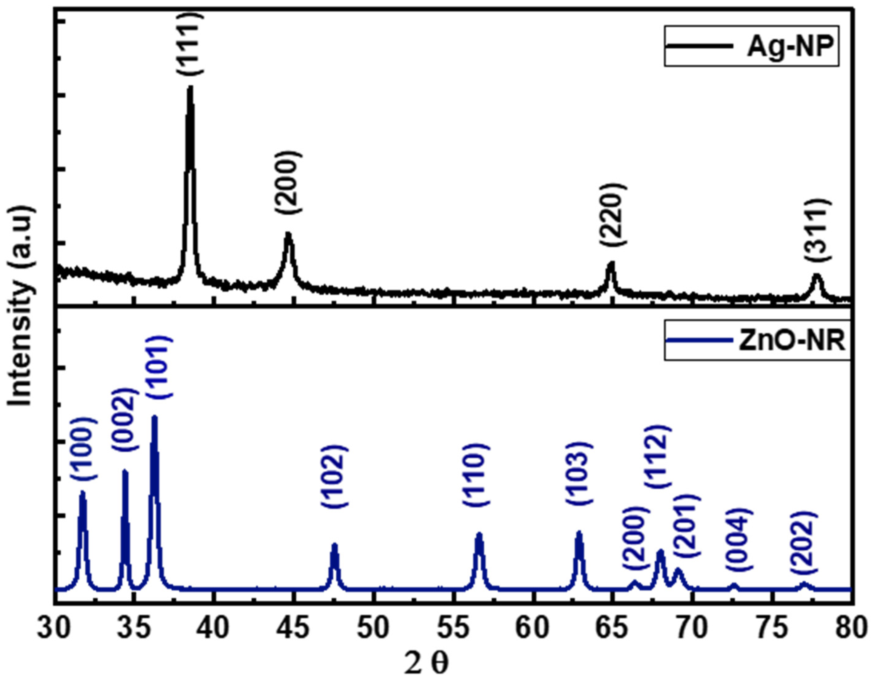
For more details about the crystal structure of the ZnO nanorods and Ag nanoparticles, see Figure 2, which illustrates a typical XRD pattern of the ZnO nanorods. The sharpness of the peaks signified the high level of crystallinity of the ZnO nanorods, demonstrating a single-phase wurtzite structure. The observed diffraction peaks were associated with the existence of a pure hexagonal phase of ZnO with lattice constants of a = 3.251 Å and c = 5.208 Å, consistent with JCPDS card for ZnO (JCPDS, 65-3411) [27]. The crystalline diameter of ZnO nanorods was approximated to be 20 nm, calculated employing the Debye–Scherer formula. This formula takes into account various factors, including the crystallite size, wavelength of the X-ray used, and the full width at half maximum (FWHM) of the observed diffraction peak. By applying this formula, we can estimate the average crystalline size of the ZnO nanorods, providing crucial information about their physical properties [28]. Furthermore, the XRD patterns of silver nanoparticles revealed peaks at 2θ angles of 38.4°, 44.7°, 64.6°, and 77.7°, corresponding to the (111), (200), (220), and (311) planes, indicating the crystalline phase of silver metal with a face-centered cubic structure, consistent with the JCPDS File No. 04-0783. These diffraction peaks allowed us to determine the orientation and arrangement of the atoms within the silver nanoparticles, providing valuable insights into their structural properties [29]. The average size of Ag nanoparticles, calculated from the full width at half maximum (FWHM) of the peak for the 111 plane, was 14.8 nm. The micro-strain (ε) for ZnO nanorods was 0.0019, while the micro-strain (ε) for AgNP was 0.0023. The micro-strain could be determined using the equation ε = βcosθ/4, where β is the line broadening and θ is the diffraction angle [28].

3.2. Kelvin Probe Force Microscopy of ZnO-NRs and AgNPs

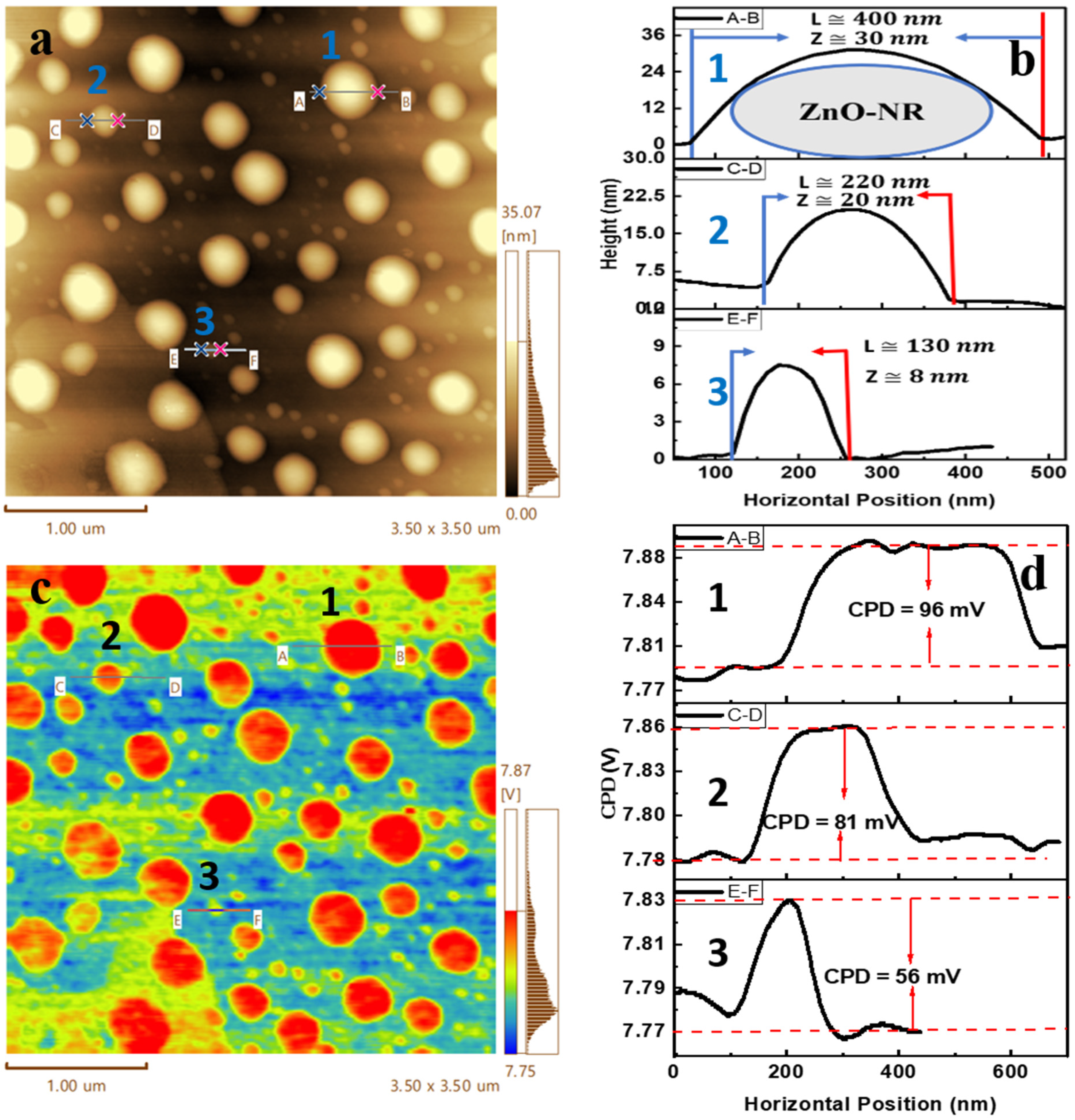
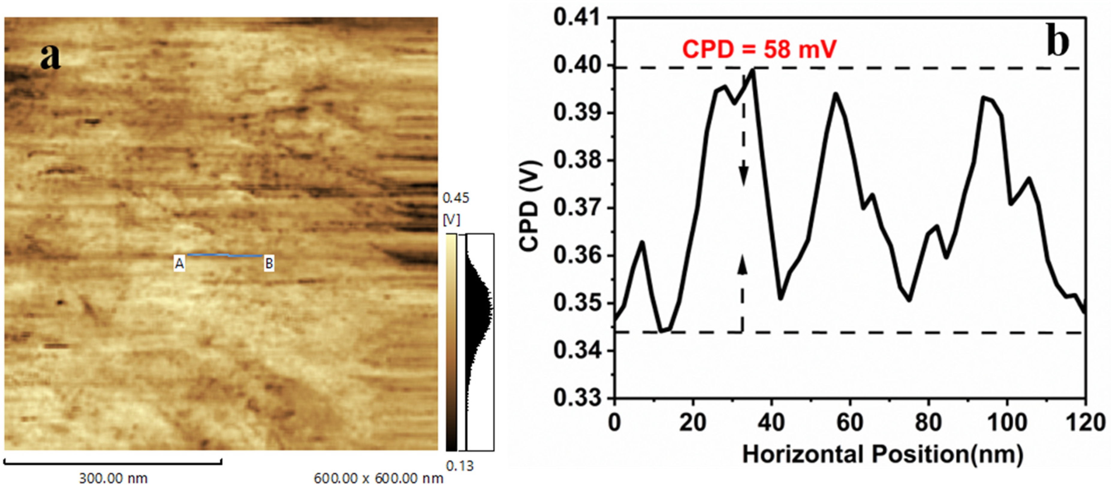
Figure 3 and Figure 4 show the KPFM characteristics of ZnO nanorods and Ag nanoparticles on a silicon substrate. The detailed images reveal the electrical interaction between the probe and the sample, with high potential shown as red and low potential as yellow for the ZnO nanorods and Ag nanoparticles. The average contact potential difference (CPD) for ZnO nanorods with a 30 nm diameter and 400 nm length was approximately 96 mV. Similarly, ZnO nanorods with a 20 nm diameter and 220 nm lengths had a contact potential difference of 81 mV. In contrast, nanorods with an 8 nm diameter and 130 nm length showed a contact potential difference of 56 mV. These results emphasized the influence of ZnO nanorod dimensions on the contact potential difference, as illustrated in Figure 3c,d. The AFM topography and KPFM images of Ag nanoparticles of varying sizes are shown in Figure 4. The average CPD for the Ag nanoparticles was 46 mV for a size of 4 nm and 70 mV for a size of 13 nm, as illustrated in Figure 4d. Figure 5 displays the KPFM for a reference sample of highly ordered pyrolytic graphite (HOPG), grade ZYA. This sample had a mosaic spread of 0.4 ± 0.1° and dimensions of 10 mm by 10 mm with a thickness of 1 mm. The average contact potential difference (CPD) for this sample was approximately 58 mV, as shown in Figure 5b. The sample was provided by (MikroMasch, Wetzlar, Germany).
The main goal of Kelvin probe force microscopy (KPFM) is to accurately measure the work function of a specific sample. A key factor in KPFM is the surface potential, which represents the difference in work function values between the sample surface, denoted as ϕ s a m p l e , and the tip of the AFM probe, represented as ϕ t i p . This difference is mathematically defined by the following equation:
ϕ s a m p l e = ϕ t i p e V C P D
where e represents the charge of a single electron, and V C P D is the contact potential difference between the probe tip and the sample’s surface [30]. To obtain an accurate assessment of the work function of ZnO nanorods, it is necessary to determine the work function of the cantilever within the apparatus. Calibration is important to ensure the reliability of measurements and typically involves the use of a reference material with a known work function for standardization purposes. In this study, highly oriented pyrolytic graphite (HOPG) was used as the reference material, with a work function range of 4.5 to 5 eV, serving as a benchmark for calibration and precision of measurements [31].
Using Equation (1), similar formulas are derived for both ZnO nanorods and HOPG substrates. The work function of the ZnO nanorods substrate is denoted as ϕ Z n O N R , and the specific contact potential difference for ZnO nanorods substrate is represented as V(CPD,ZnO-NR). Similarly, the work function for the HOPG substrate is ϕ H O P G , and its unique contact potential difference is V(CPD,HOPG). The difference between the work functions of these two substrates can be determined using the following equations:
ϕ Z n O N R = ϕ H O P G + e V C P D , H O P G V C P D , Z n O N R    
Using the Equation (2) and CPD values from the analysis in Figure 3c,d and Figure 5b and the published values for HOPG’s work function, the work function of ZnO nanorods was accurately estimated. For ZnO nanorods with approximately 30 nm diameter and 400 nm length, the work function was calculated to be 4.556 eV. Additionally, for ZnO nanorods with a diameter of around 20 nm and a length of 220 nm, the work function was estimated to be 4.527 eV. On the other hand, for ZnO nanorods with a diameter of 8 nm and a length of 130 nm, the work function was found to be 4.552 eV. Our calculation of the work function for ZnO nanorods was approximately 4.55 eV, which was higher than the work function of ZnO bulk, typically around 4.45 eV [32]. The difference in work function values observed between ZnO nanorods and bulk ZnO was attributed to various factors. Quantum confinement, influenced by the nanorods’ size, restricted electron movement, leading to higher energy levels and an increased work function. Nanorods also had a greater surface-to-volume ratio compared with bulk materials, leading to changes in electronic structure and possibly increased surface energy, resulting in a higher work function [33].
In the context of calculating the work function of silver nanoparticles, we use Equation (1) and can also create similar equations for both Ag nanoparticles and HOPG substrates. By representing the work function of the silver nanocluster substrate as ϕAg and the specific contact potential difference for the silver nanoparticles substrate as V(CPD,Ag), we can then denote the work function of the HOPG substrate as ϕHOPG and its unique contact potential difference as V(CPD,HOPG). The relationship between the work functions of silver and HOPG is connected through their respective contact potential differences:
ϕ A g = ϕ H O P G + e V C P D , H O P G V C P D , A g    
Using Equation (3) and the contact potential difference (CPD) data from Figure 4d and Figure 5b, along with the work function value of HOPG from the literature [32], the work function of the AgNPs with an average diameter of 4 nm was determined to be 4.56 eV. For nanoparticles of size 14 nm, the work function equaled 4.538 eV.
From the literature sources, the work function of bulk silver was known to be 4.3 eV, while the work function of the Ag nanocluster was 4.587 eV [34], and that of a vacuum-deposited Ag electrode was 4.68 eV. The work function of the Ag nanoparticles was estimated to be around 4.56 eV and 4.54, which aligned closely with the values reported in the literature. The remarkable findings revealed that an increase in particle size led to a significant decrease in work function due to the interesting isotropic surface curvature of the symmetrical spherical shape. Equation (4) is utilized to compute the electronic work function for a spherical particle, taking into account the work function for the plane surface, electron charge, and the permittivity of the medium. This equation emphasizes that the surface characteristics of a nanoparticle have a greater impact when the particle is smaller [35,36].
      ϕ E s = ϕ E 0 + 1 2 π ϵ   e 2 r a
The constant curvature of a spherical nanoparticle greatly increases its work function compared with a flat surface, requiring more energy to extract an electron from a surface with a higher degree of positive curvature. This compelling example effectively demonstrates the complex interaction between quantum mechanics and electrostatics on the mesmerizing nanoscale, ultimately leading to the emergence of size-specific properties distinct from those observed in bulk materials.

3.3. Current Mapping and I-V Measurements

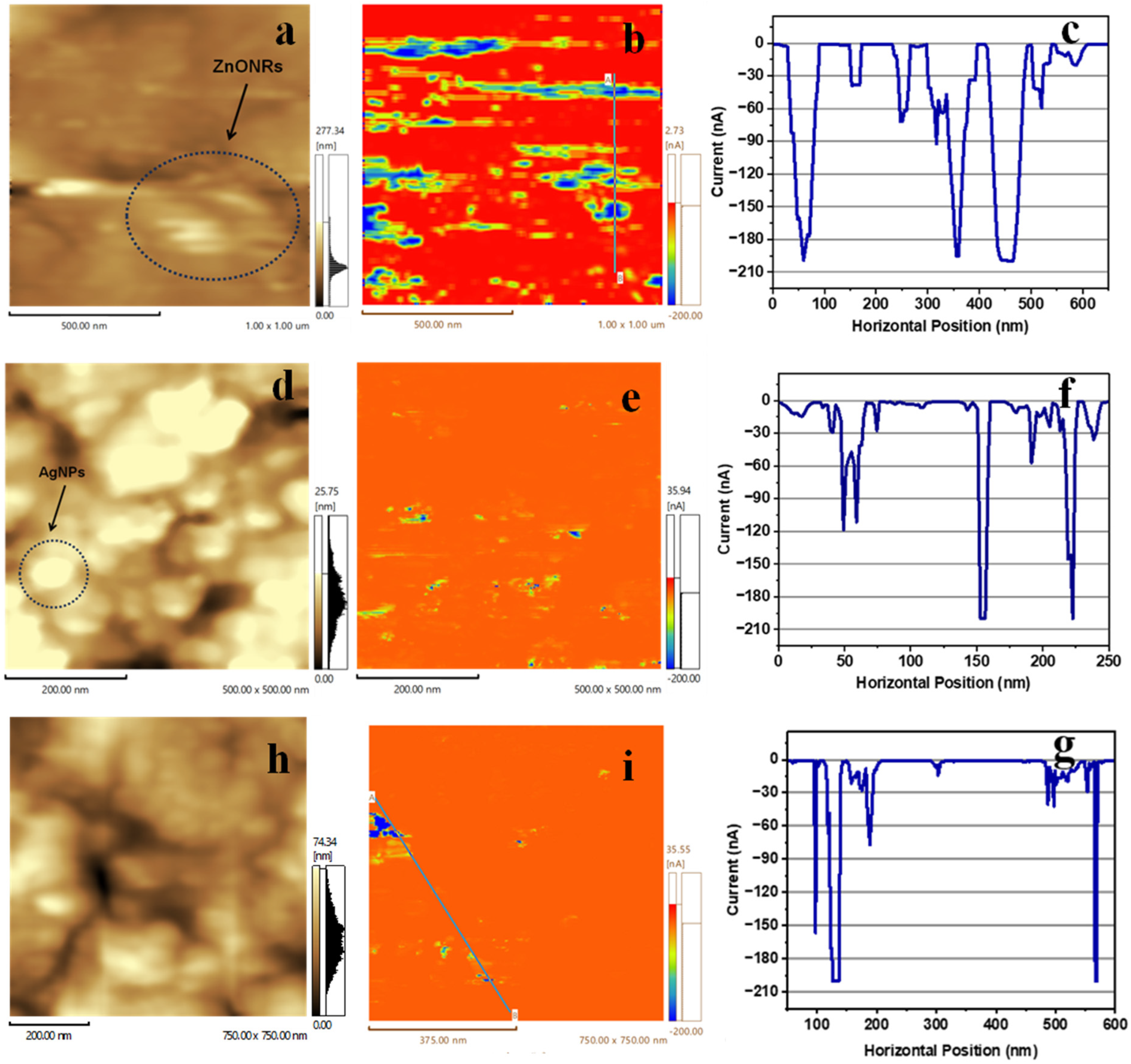
We present an electrical analysis of zinc oxide (ZnO) nanorods, silver nanoparticles (AgNPs), and a hybrid material using conductive atomic force microscopy (C-AFM). This advanced method enabled the simultaneous recording of current maps and topography obtained through contact mode AFM. Additionally, C-AFM allowed for the precise determination of the local current-voltage (I-V) characteristics of the top surface of ZnO nanorods, silver nanoparticles, and the hybrid composite material as shown in Figure 6 and Figure 7. By applying voltage through a conductive tip in contact with the ZnO nanorods’ surfaces, variations in electrical current could be detected, unveiling defects and surface states. This method enabled precise control and adjustment of the electrical properties of the ZnO nanorods.
Distinct areas with heightened and reduced current values, depicted in Figure 6c, pointed out significant regions such as defects or highly conducting pathways. Scattered yet noteworthy regions of elevated current indicated localized areas of high conductivity or possible defects, with current values equal to or exceeding 150 nA. Conversely, widespread low-current sections covered most of the image, indicating general low conductivity or a consistent baseline current level throughout the ZnO nanorods, with current values equal to or less than 10 nA. Furthermore, for Ag nanoparticles, the high-current region ranged from 120 nA to 200 nA, possibly linked to differences in their size. Similarly, for hybrid ZnO-NR and Ag-NP, the high current region fell between 160 nA and 200 nA, as seen in Figure 6g.
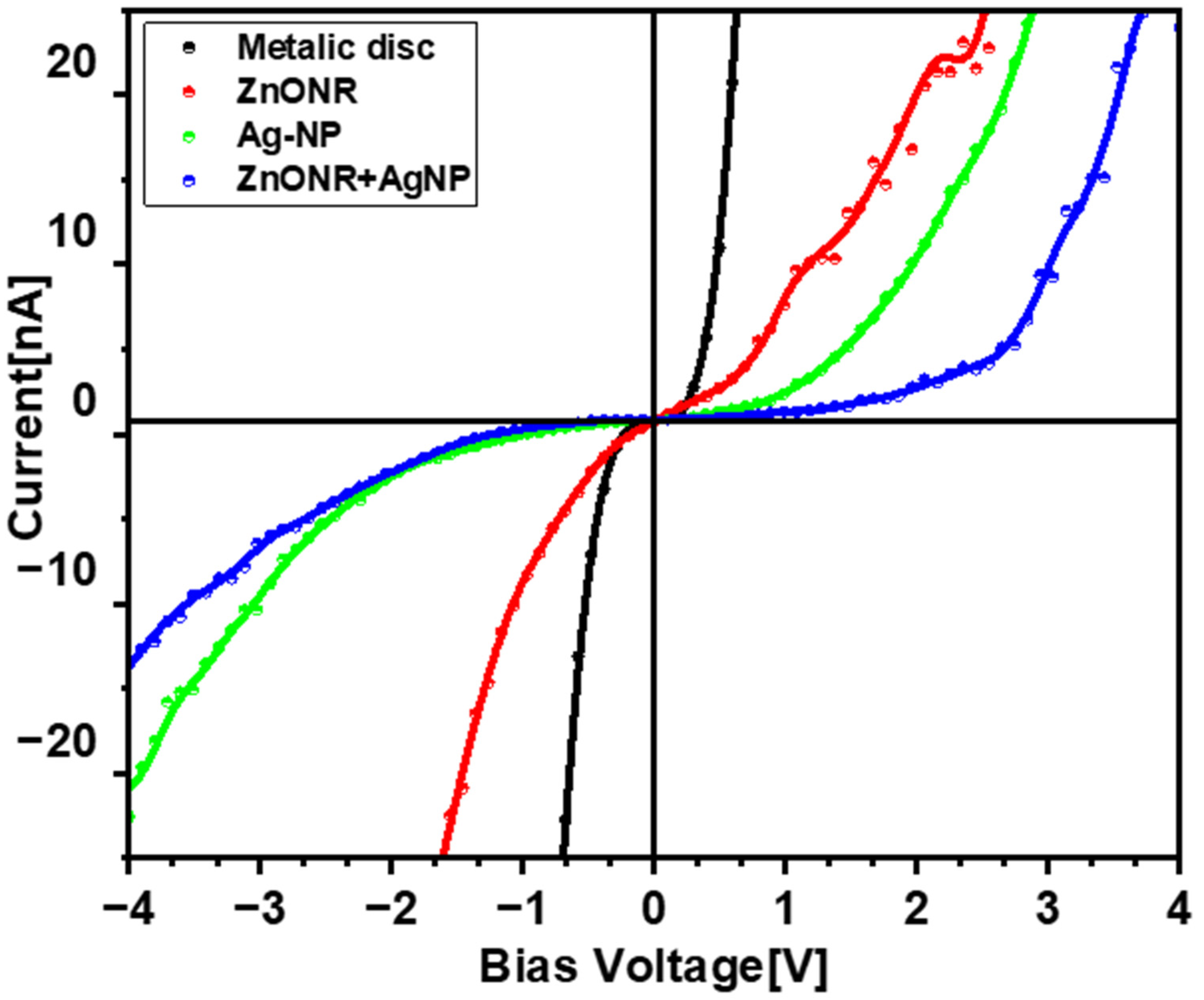
The results presented in Figure 7 show a typical I-V characteristic curve obtained from a metallic disc as a reference sample, ZnO nanorods (ZnONRs), silver nanoparticles (Ag-NPs), and a combination of ZnO-NR and Ag-NP samples. The findings revealed a significant increase in current at approximately 1 V for both ZnO-NRs and Ag-NPs, indicating turn-on voltages of around 1 V for each. When combined, there was a different turn-on voltage around 2.5 V, suggesting a unique response to the combined effect. The reverse bias analysis also highlighted the distinctive characteristics of the ZnONR and Ag-NP combination, effectively blocking the current until very high negative voltages. It is important to understand that the presence of Ag-NP significantly impacted the electrical properties of ZnONR. The observed effects in the I-V traits for ZnO nanorods (ZnONRs), silver nanoparticles (Ag-NPs), and their combination required a thorough understanding of the physical and chemical interactions between these materials.
In analyzing the reasons for the increase in the current at around 2.5 V, it is necessary to consider the intrinsic characteristics of ZnO nanorods and silver nanoparticles. ZnO is a wide-bandgap semiconductor, and in forward bias, significant current flows once the voltage exceeds the built-in potential barrier. The presence of silver nanoparticles, which are exceptional conductors, also aids in charge transport. The combination of ZnONRs with Ag-NPs can create a Schottky junction, improving carrier injection at the interface, and can slightly alter the turn-on voltage compared with individual components. The presence of Ag-NPs can introduce new surface states and modify existing defects in ZnONRs, impacting the overall conduction mechanism. Additionally, it can enhance the barrier height in reverse bias due to the Schottky effect, indicating improved stability and robustness of the device.
Furthermore, the presence of Ag-NPs can enhance the mobility of charge carriers in ZnONRs by providing additional pathways and reducing scattering [37]. It can also passivate surface defects, reducing trap states and enhancing charge transport. The interaction between Ag-NPs and ZnONRs can modify the band structure, leading to changes in electrical properties. It is important to mention that Schottky diodes can be made with higher threshold voltages using various semiconductor materials like silicon carbide (SiC) or gallium nitride (GaN) [38]. Additionally, Schottky diodes made with Au NPs and n-Si have a turn-on voltage of around 1.0 volt [39], indicating a noticeable difference in performance. On the other hand, the turn-on voltage for the Bi2S3 nanorods and Au nanoparticles device is approximately 0.72 volts [40], showing significant differences in voltage characteristics between different metal systems. However, the combination of ZnO nanorods and silver nanoparticles offers a more cost-effective synthesis option in this particular study.

3.4. Optical Properties of Hybrid of ZnO-NRs and Ag-NPs

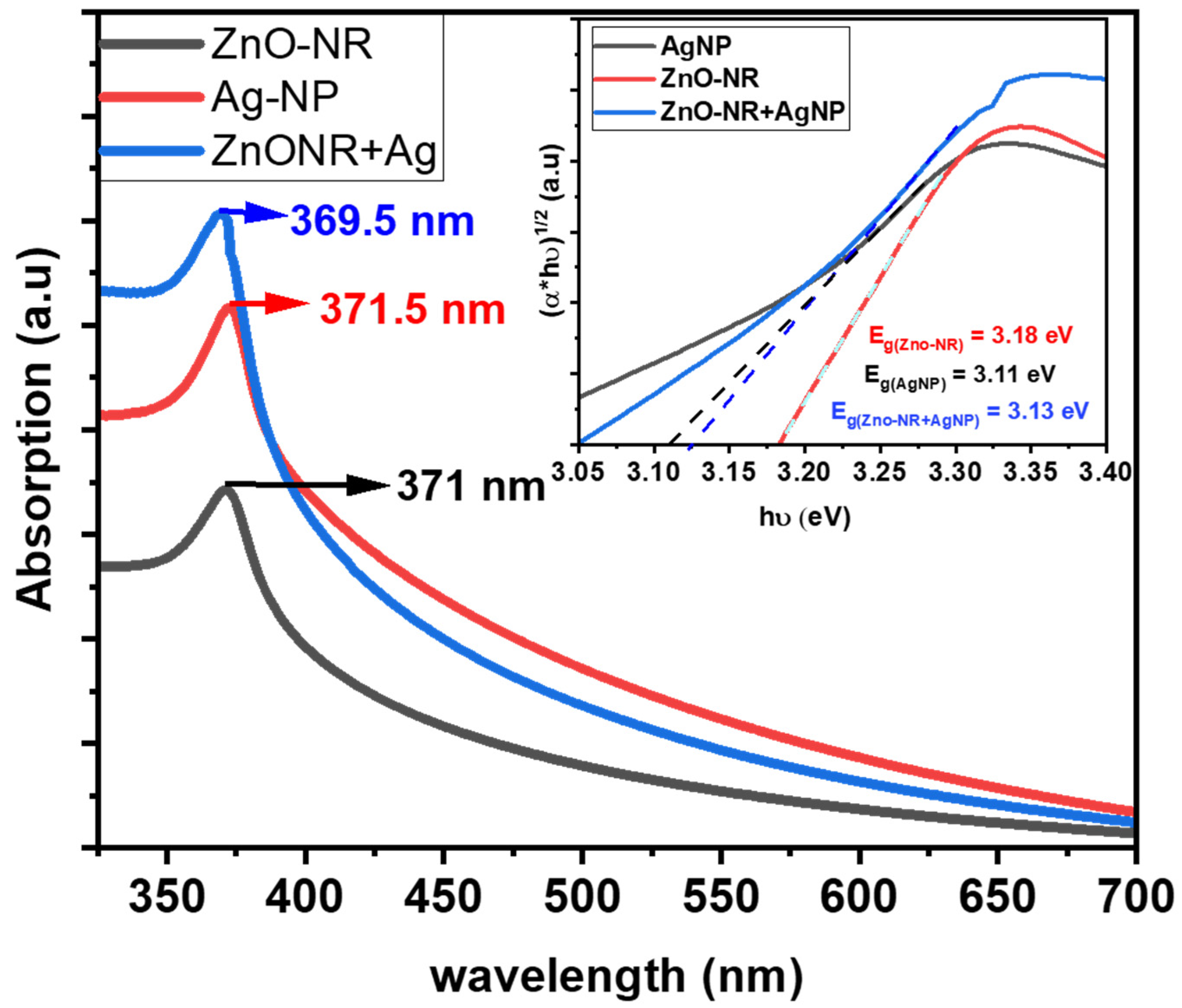
Figure 8 illustrates the UV-Vis absorption spectra of ZnO nanorods (ZnO-NRs), silver nanoparticles (Ag-NPs), and their composites (ZnO-NR + Ag), providing important insights into their optical characteristics. The distinct absorption peak at 371 nm observed in the ZnO nanorods was in line with the near-band-edge absorption of ZnO-NR. Meanwhile, the silver nanoparticles showed a slightly shifted absorption peak at 371.5 nm, attributed to the localized surface plasmon resonance (LSPR) effect. The normal LSPR peak for silver nanoparticles is typically around 390–450 nm, so this shift to around 370 nm suggested that multiple factors such as nanoparticle size, dielectric environment, and surface chemistry may have been influencing the resonance behavior. Smaller nanoparticles tend to experience a blue shift in their plasmon resonance peaks due to quantum confinement effects, leading to absorption moving toward shorter wavelengths. The refractive index of the surrounding medium also plays a significant role, with a lower index resulting in a similar blue shift in the absorption peak. Additionally, surface modifications like ligand attachment or oxidation can impact the electronic properties of the nanoparticles, causing shifts in the LSPR peak [10,41,42,43]. The absorption peak for the composite was at 369.5 nm, slightly blue-shifted compared with the individual ZnO-NR and Ag-NP spectra. The analysis of energy gaps in the inset in Figure 8 shows the ZnO nanorods (ZnO-NRs), silver nanoparticles (AgNPs), and the ZnO-NR + AgNP hybrid, as illustrated in a Tauc plot, which plots the square root of the absorption coefficient against the photon energy. ZnO nanorods are known for their distinct composition and structure, displaying a noticeable absorption peak at the bandgap energy level, typically around 3.11 eV. In contrast, Ag nanoparticles exhibit absorption traits influenced by surface plasmon resonance, with a well-defined absorption peak near 3.18 eV [44].
The alteration in the absorption spectrum when ZnO-NRs and AgNPs combined to form the ZnO-NR + AgNP hybrid was of particular interest. This change signified a close interaction between the ZnO nanorods and the Ag nanoparticles, resulting in a synergistic effect that enhanced the overall absorption performance. Specifically, the bandgap energy of the hybrid material experienced a slight shift, settling at approximately 3.13 eV. While seemingly small, this shift held great significance as it indicated the enhanced absorption capabilities of the hybrid material. The slight change in bandgap energy, approximately 3.13 eV, between the hybrid ZnO nanorods and the Ag nanoparticles was significant for several reasons. The surface plasmon resonance effect of Ag nanoparticles could enhance the electromagnetic field nearby and increase light absorption, impacting the properties of the ZnO nanorod. Additionally, the interaction between the two materials could result in charge transfer, altering the electronic structure of ZnO and causing a minor shift in bandgap energy. The size and distribution of Ag nanoparticles could also influence the electronic properties of ZnO, with quantum size effects coming into play due to the confinement of charge carriers at the nanoscale [45,46].
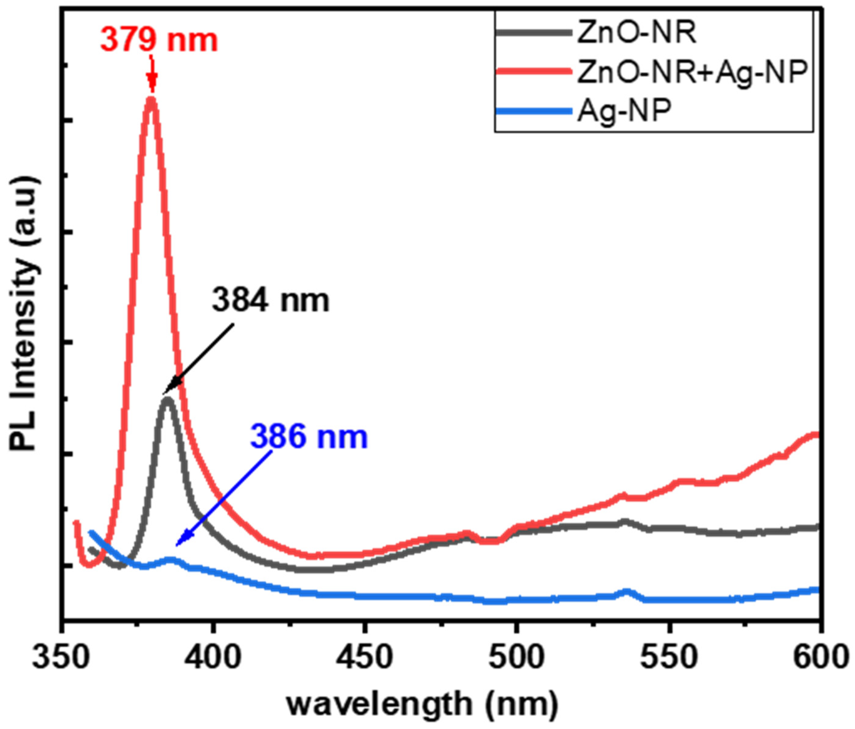
The photoluminescence spectra in Figure 9 show the presence of ZnO nanorods and Ag nanoparticles, with peaks at 384 nm and 386 nm, respectively. The addition of Ag nanoparticles at 379 nm had a significant effect on the optical characteristics of ZnO nanorods, resulting in increased photoluminescence intensity and changes in peak positions. This change was likely due to the plasmonic effects of the Ag nanoparticles and their interaction with the ZnO nanorods.
The addition of Ag nanoparticles caused a noticeable shift and change in intensity in the PL spectrum, with a shift from 379 nm to 386 nm, suggesting fundamental alterations in the electronic structure and energy states of ZnO nanorods. The heightened PL intensity for the hybrid structures indicates improved photoluminescence as a result of the strong interaction between ZnO nanorods and Ag nanoparticles.
One potential mechanism for the observed changes in PL intensity and peak positions is the surface plasmon resonance (SPR) of Ag nanoparticles, which can significantly enhance the local electromagnetic field and the PL intensity of ZnO nanorods. Another potential mechanism is the transfer of charge between the ZnO nanorods and Ag nanoparticles, which can affect the recombination rate of electron–hole pairs in ZnO, leading to variations in PL intensity and peak positions [47,48].

4. Conclusions

The detailed analysis of ZnO nanorods and silver nanoparticles provided valuable insights into their physical, structural, electrical, and optical characteristics. Utilizing scanning probe microscopy (SPM) and X-ray diffraction (XRD), it was determined that the ZnO nanorods exhibited a distinct shape, with lengths of around 350 nm and a highly crystalline, single-phase wurtzite structure. The silver nanoparticles, on the other hand, displayed a spherical shape with heights ranging from 5 to 14 nm and were confirmed to be composed of silver metal with a face-centered cubic structure. Kelvin probe force microscopy (KPFM) measurements offered further insights into the work function and contact potential differences (CPDs) of these nanomaterials. It was revealed that the work function of ZnO nanorods varied with size, ranging from approximately 4.556 eV to 4.527 eV, while the work function of Ag nanoparticles ranged from 4.56 eV to 4.538 eV. Conductive atomic force microscopy (C-AFM) was employed to investigate the electrical properties of these materials, uncovering regions of both high and low current in both the ZnO nanorods and the Ag nanoparticles. The hybrid ZnO-NR and Ag-NP material exhibited a unique electrical response, with a combined turn-on voltage of around 2.5 V. The optical properties of the ZnO-NR and Ag-NP hybrid were examined through absorption and photoluminescence (PL) spectra. The hybrid material demonstrated enhanced absorption capabilities, a shift in bandgap energy, and alterations in the photoluminescence peak and intensity. These findings highlight the positive impact of the hybridization of ZnO-NR and Ag-NP on their optical and electrical properties, positioning them as promising candidates for advanced nanotechnology applications.

Funding

This research received no external funding.

Data Availability Statement

The data that support the findings of this study are available from the corresponding author upon request.

Acknowledgments

The author thanks Palestine Technical University—Kadoorie (PTUK) and the Palestinian Ministry of Higher Education for facilities and support.

Conflicts of Interest

The author declare no conflict of interest.

References

  1. Que, M.; Lin, C.; Sun, J.; Chen, L.; Sun, X.; Sun, Y. Progress in ZnO Nanosensors. Sensors 2021, 21, 5502. [Google Scholar] [CrossRef] [PubMed]
  2. Wu, Y.; Ma, Y.; Zheng, H.; Ramakrishna, S. Piezoelectric Materials for Flexible and Wearable Electronics: A Review. Mater. Des. 2021, 211, 110164. [Google Scholar] [CrossRef]
  3. Putri, A.E.; Roza, L.; Budi, S.; Ali Umar, A.; Fauzia, V. Tuning the Photocatalytic Activity of Nanocomposite ZnO Nanorods by Shape-Controlling the Bimetallic AuAg Nanoparticles. Appl. Surf. Sci. 2021, 536, 147847. [Google Scholar] [CrossRef]
  4. Lefatshe, K.; Dube, P.; Sebuso, D.; Madhuku, M.; Muiva, C. Optical Dispersion Analysis of Template Assisted 1D-ZnO Nanorods for Optoelectronic Applications. Ceram. Int. 2021, 47, 7407–7415. [Google Scholar] [CrossRef]
  5. Onyszko, M.; Zywicka, A.; Wenelska, K.; Mijowska, E. Revealing the Influence of the Shape, Size, and Aspect Ratio of ZnO Nanoparticles on Antibacterial and Mechanical Performance of Cellulose Fibers Based Paper. Part. Part. Syst. Charact. 2022, 39, 2200014. [Google Scholar] [CrossRef]
  6. Boulahlib, S.; Dib, K.; Özacar, M.; Bessekhouad, Y. Optical, Dielectric, and Transport Properties of Ag-Doped ZnO Prepared by Aloe Vera Assisted Method. Opt. Mater. 2021, 113, 110889. [Google Scholar] [CrossRef]
  7. Abutalib, M.M.; Rajeh, A. Influence of ZnO/Ag Nanoparticles Doping on the Structural, Thermal, Optical and Electrical Properties of PAM/PEO Composite. Phys. B Condens. Matter 2020, 578, 411796. [Google Scholar] [CrossRef]
  8. Sharma, V.; Verma, D.; Okram, G.S. Influence of Surfactant, Particle Size and Dispersion Medium on Surface Plasmon Resonance of Silver Nanoparticles. J. Phys. Condens. Matter 2020, 32, 145302. [Google Scholar] [CrossRef]
  9. Mehata, M.S. Green Route Synthesis of Silver Nanoparticles Using Plants/Ginger Extracts with Enhanced Surface Plasmon Resonance and Degradation of Textile Dye. Mater. Sci. Eng. B 2021, 273, 115418. [Google Scholar] [CrossRef]
  10. Alzoubi, F.Y.; Ahmad, A.A.; Aljarrah, I.A.; Migdadi, A.B.; Al-Bataineh, Q.M. Localize Surface Plasmon Resonance of Silver Nanoparticles Using Mie Theory. J. Mater. Sci. Mater. Electron. 2023, 34, 2128. [Google Scholar] [CrossRef]
  11. Juma, M.W.; Birech, Z.; Mwenze, N.M.; Ondieki, A.M.; Maaza, M.; Mokhotjwa, S.D. Localized Surface Plasmon Resonance Sensing of Trenbolone Acetate Dopant using Silver Nanoparticles. Sci. Rep. 2024, 14, 5721. [Google Scholar] [CrossRef]
  12. Checa, M.; Neumayer, S.M.; Tsai, W.-Y.; Collins, L. Advanced Modes of Electrostatic and Kelvin Probe Force Microscopy for Energy Applications. In Atomic Force Microscopy for Energy Research; CRC Press: Boca Raton, FL, USA, 2022; ISBN 978-1-00-317404-2. [Google Scholar]
  13. Wang, J.; Zhang, H.; Cao, G.; Xie, L.; Huang, W. Injection and Retention Characterization of Trapped Charges in Electret Films by Electrostatic Force Microscopy and Kelvin Probe Force Microscopy. Phys. Status Solidi A 2020, 217, 2000190. [Google Scholar] [CrossRef]
  14. Li, X.; Hu, X.; Liu, M.; Sun, L.; Qiu, X. Electrical Characteristics of a Carbon Nanotube-Functionalized Probe for Kelvin Probe Force Microscopy. J. Phys. Chem. C 2020, 124, 28261–28266. [Google Scholar] [CrossRef]
  15. Jakob, D.S.; Li, N.; Zhou, H.; Xu, X.G. Integrated Tapping Mode Kelvin Probe Force Microscopy with Photoinduced Force Microscopy for Correlative Chemical and Surface Potential Mapping. Small 2021, 17, 2102495. [Google Scholar] [CrossRef]
  16. Hackl, T.; Poik, M.; Schitter, G. Heterodyne AC Kelvin Probe Force Microscopy for Nanoscale Surface Potential Imaging in Liquids. IEEE Trans. Instrum. Meas. 2023, 72, 1–8. [Google Scholar] [CrossRef]
  17. Grévin, B.; Husainy, F.; Aldakov, D.; Aumaître, C. Dual-Heterodyne Kelvin Probe Force Microscopy. Beilstein J. Nanotechnol. 2023, 14, 1068–1084. [Google Scholar] [CrossRef]
  18. Maryon, O.O.; Efaw, C.M.; DelRio, F.W.; Graugnard, E.; Hurley, M.F.; Davis, P.H. Co-Localizing Kelvin Probe Force Microscopy with Other Microscopies and Spectroscopies: Selected Applications in Corrosion Characterization of Alloys. J. Vis. Exp. 2022, 184, 64102. [Google Scholar] [CrossRef]
  19. Lee, H.; Lee, W.; Lee, J.H.; Yoon, D.S. Surface Potential Analysis of Nanoscale Biomaterials and Devices Using Kelvin Probe Force Microscopy. J. Nanomater. 2016, 2016, 4209130. [Google Scholar] [CrossRef]
  20. Beinik, I.; Kratzer, M.; Wachauer, A.; Wang, L.; Lechner, R.T.; Teichert, C.; Motz, C.; Anwand, W.; Brauer, G.; Chen, X.Y.; et al. Electrical Properties of ZnO Nanorods Studied by Conductive Atomic Force Microscopy. J. Appl. Phys. 2011, 110, 052005. [Google Scholar] [CrossRef]
  21. Fernando, P.S.; Mativetsky, J.M. Unambiguous Measurement of Local Hole Current in Organic Semiconductors Using Conductive Atomic Force Microscopy. J. Phys. Chem. C 2023, 127, 9903–9910. [Google Scholar] [CrossRef]
  22. Caballero-Quintana, I.; Amargós-Reyes, O.; Maldonado, J.-L.; Nicasio-Collazo, J.; Romero-Borja, D.; Barreiro-Argüelles, D.; Molnár, G.; Bousseksou, A. Scanning Probe Microscopy Analysis of Nonfullerene Organic Solar Cells. ACS Appl. Mater. Interfaces 2020, 12, 29520–29527. [Google Scholar] [CrossRef]
  23. Khoury, R.; Alvarez, J.; Ohashi, T.; Martín, I.; Ortega, P.; Lopez, G.; Jin, C.; Li, Z.; Rusli; Bulkin, P.; et al. Observation of Photovoltaic Effect within Locally Doped Silicon Nanojunctions Using Conductive Probe AFM. Nano Energy 2020, 76, 105072. [Google Scholar] [CrossRef]
  24. Barrigón, E.; Hrachowina, L.; Borgström, M.T. Light Current-Voltage Measurements of Single, as-Grown, Nanowire Solar Cells Standing Vertically on a Substrate. Nano Energy 2020, 78, 105191. [Google Scholar] [CrossRef]
  25. Musa, I.; Qamhieh, N.; Mahmoud, S.T. Synthesis and Length Dependent Photoluminescence Property of Zinc Oxide Nanorods. Results Phys. 2017, 7, 3552–3556. [Google Scholar] [CrossRef]
  26. Musa, I.; Mousa, R. Synthesis and Characterization of Variable-Sized Silver Nanoparticles Using Pistacia Palaestina Leaf Extract. Plasmonics 2024, 1–9. [Google Scholar] [CrossRef]
  27. Meena, P.L.; Bhardwaj, P.; Kumar, Y.; Singh, S.P. Synthesis and Characterization of One Dimensional ZnO Nanorods. In Proceedings of the AIP Conference Proceedings, Longowal, India, 9–11 November 2021; Volume 2352, p. 040043. [Google Scholar] [CrossRef]
  28. Musa, I.; Qamhieh, N. Study of optical energy gap and quantum confinment effects in zinc oxide nanoparticles and nanorods. Dig. J. Nanomater. Biostruct. 2019, 14, 119–125. [Google Scholar]
  29. Ali, H.; Azad, A.K.; Khan, K.A.; Rahman, O.; Chakma, U.; Kumer, A. Analysis of Crystallographic Structures and Properties of Silver Nanoparticles Synthesized Using PKL Extract and Nanoscale Characterization Techniques. ACS Omega 2023, 8, 28133–28142. [Google Scholar] [CrossRef]
  30. Glatzel, T.; Gysin, U.; Meyer, E. Kelvin Probe Force Microscopy for Material Characterization. Microscopy 2022, 71, i165–i173. [Google Scholar] [CrossRef] [PubMed]
  31. Musa, I.; Faqi, R. Structural, Electrostatic Force Microscopy, Work Function, and Optical Characterization of Pure and Al-Doped ZnO Nanoparticles. Results Mater. 2024, 22, 100570. [Google Scholar] [CrossRef]
  32. Mishra, Y.K.; Chakravadhanula, V.S.K.; Hrkac, V.; Jebril, S.; Agarwal, D.C.; Mohapatra, S.; Avasthi, D.K.; Kienle, L.; Adelung, R. Crystal Growth Behaviour in Au-ZnO Nanocomposite under Different Annealing Environments and Photoswitchability. J. Appl. Phys. 2012, 112, 064308. [Google Scholar] [CrossRef]
  33. Sahana, M.B.; Sudakar, C.; Dixit, A.; Thakur, J.S.; Naik, R.; Naik, V.M. Quantum Confinement Effects and Band Gap Engineering of SnO2 Nanocrystals in a MgO Matrix. Acta Mater. 2012, 60, 1072–1078. [Google Scholar] [CrossRef]
  34. Musa, I.; Qamhieh, N.; Mahmoud, S.T. Ag Nanocluster Production through DC Magnetron Sputtering and Inert Gas Condensation: A Study of Structural, Kelvin Probe Force Microscopy, and Optical Properties. Nanomaterials 2023, 13, 2758. [Google Scholar] [CrossRef]
  35. Makov, G.; Nitzan, A.; Brus, L.E. On the Ionization Potential of Small Metal and Dielectric Particles. J. Chem. Phys. 1988, 88, 5076–5085. [Google Scholar] [CrossRef]
  36. Musa, I.; Ghabboun, J. Work Function, Electrostatic Force Microscopy, Tunable Photoluminescence of Gold Nanoparticles, and Plasmonic Interaction of Gold Nanoparticles/Rhodamine 6G Nanocomposite. Plasmonics 2024, 1–10. [Google Scholar] [CrossRef]
  37. Thappily, P.; Mandin, P.; Sauvage, T.; Sandhya, K. Enhancement of Charge Transport Properties of a Novel Rubbery Semiconductor via Silver Nanocomplexing. Mater. Sci. Semicond. Process. 2021, 131, 105854. [Google Scholar] [CrossRef]
  38. Kumar, A.; Moradpour, M.; Losito, M.; Franke, W.-T.; Ramasamy, S.; Baccoli, R.; Gatto, G. Wide Band Gap Devices and Their Application in Power Electronics. Energies 2022, 15, 9172. [Google Scholar] [CrossRef]
  39. Abbas, Y.; Rezk, A.; Anwer, S.; Saadat, I.; Nayfeh, A.; Rezeq, M. Improved Figures of Merit of Nano-Schottky Diode by Embedding and Characterizing Individual Gold Nanoparticles on n-Si Substrates. Nanotechnology 2020, 31, 125708. [Google Scholar] [CrossRef]
  40. Saha, S.K.; Pal, A.J. Schottky Diodes between Bi2S3 Nanorods and Metal Nanoparticles in a Polymer Matrix as Hybrid Bulk-Heterojunction Solar Cells. J. Appl. Phys. 2015, 118, 014503. [Google Scholar] [CrossRef]
  41. Link, S.; El-Sayed, M.A. Size and Temperature Dependence of the Plasmon Absorption of Colloidal Gold Nanoparticles. J. Phys. Chem. B 1999, 103, 4212–4217. [Google Scholar] [CrossRef]
  42. Wu, Q.; Si, M.; Zhang, B.; Zhang, K.; Li, H.; Mi, L.; Jiang, Y.; Rong, Y.; Chen, J.; Fang, Y. Strong Damping of the Localized Surface Plasmon Resonance of Ag Nanoparticles by Ag2O. Nanotechnology 2018, 29, 295702. [Google Scholar] [CrossRef]
  43. Mulvaney, P. Surface Plasmon Spectroscopy of Nanosized Metal Particles. Langmuir 1996, 12, 788–800. [Google Scholar] [CrossRef]
  44. Campos, A.; Troc, N.; Cottancin, E.; Pellarin, M.; Weissker, H.-C.; Lermé, J.; Kociak, M.; Hillenkamp, M. Plasmonic Quantum Size Effects in Silver Nanoparticles Are Dominated by Interfaces and Local Environments. Nat. Phys. 2019, 15, 275–280. [Google Scholar] [CrossRef]
  45. Mandal, S.; Ananthakrishnan, R. Double Effects of Interfacial Ag Nanoparticles in a ZnO Multipod@Ag@Bi2S3 Z-Scheme Photocatalytic Redox System: Concurrent Tuning and Improving Charge-Transfer Efficiency. Inorg. Chem. 2020, 59, 7681–7699. [Google Scholar] [CrossRef] [PubMed]
  46. Liu, C.; Xu, X.; Wang, C.; Qiu, G.; Ye, W.; Li, Y.; Wang, D. ZnO/Ag Nanorods as a Prominent SERS Substrate Contributed by Synergistic Charge Transfer Effect for Simultaneous Detection of Oral Antidiabetic Drugs Pioglitazone and Phenformin. Sens. Actuators B Chem. 2020, 307, 127634. [Google Scholar] [CrossRef]
  47. Wang, X.; Ye, Q.; Bai, L.-H.; Su, X.; Wang, T.-T.; Peng, T.-W.; Zhai, X.-Q.; Huo, Y.; Wu, H.; Liu, C.; et al. Enhanced UV Emission from ZnO on Silver Nanoparticle Arrays by the Surface Plasmon Resonance Effect. Nanoscale Res. Lett. 2021, 16, 8. [Google Scholar] [CrossRef]
  48. Rauwel, P.; Galeckas, A.; Rauwel, E. Enhancing the UV Emission in ZnO–CNT Hybrid Nanostructures via the Surface Plasmon Resonance of Ag Nanoparticles. Nanomaterials 2021, 11, 452. [Google Scholar] [CrossRef]
Figure 1. (a) Atomic force microscopy (AFM) topography images of ZnO nanorods on a Si substrate. Scan sizes: (2.33 μm × 2.33 μm). (b) Three-dimensional projection topography of ZnO-NR. (c) Line profiles for ZnO-NRs identified in the image in (b). (d) AFM topography image of Ag nanoparticles on a mica substrate. Scan sizes: (4 μm × 4 μm). (e) Three-dimensional projection topography of Ag-NP. (f) Line profiles for AgNP identified in the image in (e). (g) AFM topography image of hybrid Ag NP and ZnO NR on a Si substrate. Scan sizes: (1.5 μm × 1.5 μm). (h) Three-dimensional projection topography of hybrid Ag NP and ZnO-NR. (i) Line profiles for AgNP identified in the image in (h).
Surfaces 07 00050 g001
Figure 2. The XRD pattern of ZnO nanorods and Ag nanoparticles.
Surfaces 07 00050 g002
Figure 3. (a) AFM topography images of ZnO nanorods on a Si substrate. Scan sizes: (3.5 μm × 3.5 μm). (b) Line profiles for variable size and length of ZnO-NRs identified in the image in (a). (c) Surface potential images of ZnO NRs deposited on the silicon substrate. (d) CPD line profiles for different sizes and lengths of ZnO NRs identified in the image in (c).
Surfaces 07 00050 g003
Figure 4. (a) AFM topography images of Ag nanoparticles on a Si substrate. Scan sizes: (3.5 μm × 3.5 μm). (b) Line profiles for variable Ag nanoparticles identified in the image in (a). (c) Surface potential images of Ag nanoparticles deposited on the silicon substrate. (d) CPD line profiles for different sizes of Ag nanoparticles identified in the image in (c).
Surfaces 07 00050 g004
Figure 5. (a) Surface potential of reference sample highly ordered pyrolytic graphite (HOPG) and (b) height profile (CPD) of HOPG extract from image (a).
Surfaces 07 00050 g005
Figure 6. (a) AFM topography images of ZnO nanorods on a metallic disc substrate. Scan sizes: (1 μm × 1 μm). (b) Current mapping of ZnO-NR. (c) Line profiles of current for ZnO-NRs identified in the image in (b). (d) AFM topography image of Ag nanoparticles on a metallic disc substrate. Scan sizes: (0.5 μm × 0.5 μm). (e) Current mapping of Ag-NP. (f) Line profiles of current for AgNP identified in the image in (e). (g) AFM topography image of hybrid Ag NP and ZnO NR on a metallic disc substrate. Scan sizes: (0.75 μm × 0.75 μm). (h) Current mapping of hybrid Ag NP and ZnO-NR. (g) Line profiles of current for AgNP and ZnO-NR identified in the image in (i).
Surfaces 07 00050 g006
Figure 7. Local I-V characteristic of metallic disc (reference), ZnO nanorods, Ag nanoparticles, and hybrid ZnO-NRs and Ag NPs.
Surfaces 07 00050 g007
Figure 8. The absorption spectrum of ZnO nanorods, Ag nanoparticles, and hybrid ZnO-NR and Ag NPs. Inset figure: (αℎυ)1/2 vs. photon energy of ZnO nanorods, Ag nanoparticles, and hybrid ZnO-NRs and Ag NPs.
Surfaces 07 00050 g008
Figure 9. The photoluminescence spectrum o of ZnO nanorods, Ag nanoparticles, and hybrid ZnO-NRs and Ag NPs.
Surfaces 07 00050 g009
Disclaimer/Publisher’s Note: The statements, opinions and data contained in all publications are solely those of the individual author(s) and contributor(s) and not of MDPI and/or the editor(s). MDPI and/or the editor(s) disclaim responsibility for any injury to people or property resulting from any ideas, methods, instructions or products referred to in the content.