Article

Material Structure and Mechanical Properties of Silicon Nitride and Silicon Oxynitride Thin Films Deposited by Plasma Enhanced Chemical Vapor Deposition

1
School of Materials Science and Engineering, Nanyang Technological University, Singapore 639798, Singapore
2
School of Materials Science and Engineering, Liaocheng University, Liaocheng 252000, China
*
Author to whom correspondence should be addressed.
Surfaces 2018, 1(1), 59-72; https://doi.org/10.3390/surfaces1010006
Submission received: 9 May 2018 / Revised: 22 August 2018 / Accepted: 27 August 2018 / Published: 30 August 2018

Abstract

:
Silicon nitride and silicon oxynitride thin films are widely used in microelectronic fabrication and microelectromechanical systems (MEMS). Their mechanical properties are important for MEMS structures; however, these properties are rarely reported, particularly the fracture toughness of these films. In this study, silicon nitride and silicon oxynitride thin films were deposited by plasma enhanced chemical vapor deposition (PECVD) under different silane flow rates. The silicon nitride films consisted of mixed amorphous and crystalline Si3N4 phases under the range of silane flow rates investigated in the current study, while the crystallinity increased with silane flow rate in the silicon oxynitride films. The Young’s modulus and hardness of silicon nitride films decreased with increasing silane flow rate. However, for silicon oxynitride films, Young’s modulus decreased slightly with increasing silane flow rate, and the hardness increased considerably due to the formation of a crystalline silicon nitride phase at the high flow rate. Overall, the hardness, Young modulus, and fracture toughness of the silicon nitride films were greater than the ones of silicon oxynitride films, and the main reason lies with the phase composition: the SiNx films were composed of a crystalline Si3N4 phase, while the SiOxNy films were dominated by amorphous Si–O phases. Based on the overall mechanical properties, PECVD silicon nitride films are preferred for structural applications in MEMS devices.

Graphical Abstract

1. Introduction

Silicon nitride (SiNx) and silicon oxynitride (SiOxNy) thin films deposited by plasma enhanced chemical vapor deposition (PECVD) are widely used in electronic device applications including passivation, isolation, insulation, and etch masking. They are also increasingly employed in microelectromechanical systems (MEMS) as functional structures in the form of beams, bridges, and membranes [1,2,3,4,5,6]. The mechanical properties of the thin films are very important to the design and reliability of the devices. Various studies have been conducted to evaluate the films’ mechanical properties including Young’s modulus, residual stress and hardness, etc. [7,8]. Adhesion of silicon oxide and nitride to substrate (such as copper) employed in micro- or nano-electronics has also been studied [9,10]. Compared with bulk samples made by powder sintering, data for the mechanical properties of silicon nitride thin films are limited and scattered. This is due to the fact that the properties of the films are closely related to the film composition, density, and microstructure, which are dependent on the deposition condition. Among existing reports, Dong et al. [5] found that the Young’s modulus of a radio frequency (RF) magnetron sputtered amorphous silicon oxynitride film was 122 GPa. Danaie et al. used a low frequency PECVD reactor to prepare silicon oxynitride films with controllable residual stresses via different gas flow rates [6]. Yau et al. [8] also employed an RF magnetron sputtering method to prepare silicon nitride films under different nitrogen flow rates. The films were amorphous and the nitrogen content was found to have decreased with increasing nitrogen flow rate. The elastic modulus showed a decreasing trend with increasing nitrogen flow rate in the range of 130–155 GPa.
Clearly, the film properties strongly depend on the microstructures, which vary with the deposition method and processing parameters [5,6,7,8,9,10,11,12]. Therefore, a systematic analysis of the correlation among composition, microstructure, and mechanical properties is necessary for our chosen PECVD method. In particular, fracture strength and fracture toughness of the silicon nitride and silicon oxynitride films are very important in designing against device failure, but the work in this area is scarce. In fact, to the best of our knowledge, there has been no report available for the fracture toughness of silicon nitride and silicon oxynitride thin films. Most of the published work on fracture toughness of silicon nitride was carried out on bulk specimens using a conventional fracture mechanics test [13,14], and the focus was mainly on the effect of doping [15,16]. However, the fracture toughness of thin films can be very different from the ones measured from bulk materials due to the difference in microstructure and composition. In the available reports on thin film fracture toughness and fracture strength studies on silicon nitride, micro-bridge [17] or micro-bulge specimens [18] had to be fabricated by a lithographic approach, which is both expensive in sample making and inaccurate in result interpretation. For example, in the micro-bridge test, the residual stress in the films had to be estimated in order to calculate the fracture toughness of the thin film [19]. Due to the uncertainty on the residual stresses, the reported value for the critical stress intensity factor ranges from 1.8 ± 0.3 MPa⋅m½ for low-stress film to an upper bound value of 14 MPa⋅m½ for a high-stress film [17]. The micro-bulge test [18], however, can only yield information on the biaxial modulus and tensile fracture strength, not the fracture toughness of the film. No report is available for the fracture toughness and fracture strength of silicon oxynitride thin films.
In this paper, the chemical composition, bonding state, microstructure, and mechanical properties of silicon nitride and oxynitride thin films, prepared by PECVD under varying silane flow rate, were studied. The mechanical properties include Young’s modulus, nano-indentation hardness and fracture toughness. The correlation between the mechanical properties and materials’ structural factors was established.

2. Materials and Methods

Silicon nitride and oxynitride films were prepared by PECVD at 200 °C on Si (100) substrates. All thin film samples were prepared on the silicon substrate except for the fracture toughness measurement, which will be described later. Prior to the deposition, the substrates were pre-cleaned with acetone, alcohol, and de-ionized water, followed by a nitrogen blow-dry using a static neutralizing blow-off gun. The silicon oxynitride films were synthesized by introducing silane (SiH4) and nitrous oxide (N2O) gases into the deposition chamber. The silicon nitride films were prepared using SiH4 with ammonia (NH3) gases. In each case, the silane flow rate was varied while other deposition parameters remained unchanged. Details of the deposition parameters are given in Table 1. All these deposition parameters were chosen on the basis of the available BKM (best known method) parameters in the industry.
The thickness of the as-deposited films was measured using a Tencor P-10 surface profilometer (ClassOne Equipment, Atlanta, GA, USA). The phases of the thin films were identified by X-ray diffractometer (XRD-6000, SHIMADZU, Kyoto, Japan) using Cu Kα radiation (wavelength of 1.54 Å) at 50 kV and 20 mA with a thin film goniometer (Rigaku, Tokyo, Japan) at a glancing angle of 1°. The chemical states of the atomic species and atomic ratio in the thin films were analyzed by XPS (Kratos AXIS spectrometer, Manchester, UK) with the monochromatic Al Kα X-ray radiation at 1486.71 eV. The base vacuum in the XPS analysis chamber was about 10−9 Torr. The samples were also analyzed using Fourier transform infrared spectroscopy (FTIR) with a Perkin Elmer system 2000 FTIR spectrometer (Waltham, MA, USA). The spectra were taken in transmission mode at normal incidence. Young’s modulus and hardness of the thin films were obtained by nanoindentation (NanotestTM, Wrexham, UK). A diamond Berkovich indenter (three-faced pyramid) was used, and the maximum depth was controlled to be around 20 nm to eliminate the possible influence from the substrate. Detailed information on the determination of the Young’s modulus and hardness using the nanoindentation method is provided in the Supporting Information (Figure S1 and Equations (S1)–(S3)).
The fracture toughness of the thin films was measured using a controlled buckling test. Details about the test are available in existing reports [19,20]. To prepare the controlled buckling beam specimens, polyetherimide (Ultem®, SABIC Asia Pacific Pte. Ltd., Singapore) was used as the substrate so that the test-piece has the required flexibility for the buckling test. A schematic illustration of the test is shown in Figure S2 in the Supporting Information. The dimensions of the samples were 48 mm × 3 mm × 0.175 mm. Five to ten samples were tested for each deposition condition. The Young’s modulus and Poisson ratio of the Ultem® substrate were 2.6 GPa and 0.36, respectively. The ratio of the thickness of the tested films to the thickness of the substrate was between 1:500 to 1:1000. The small ratio in thicknesses was to ensure that the one-side coated thin films were under uniform tensile stress through the thickness when the film-on-substrate beam bent during the experiment. For the fracture toughness measurement, the film was placed on the tension side of the bending beam. The test jig was placed on the platform of an optical microscope so that the initiation of cracking in the thin film could be directly observed [19]. The film fracture was expected to occur at the point of maximum curvature at the center of the test piece. Based on the lateral displacement at crack initiation, the fracture strain (or stress) and fracture toughness could be calculated [19,20,21]. There was a small amount of residual stress in the coated films. This stress was calibrated [22] in the fracture toughness calculation. The fracture toughness, in terms of the critical energy release rate, GIC, is given by
G Ic = 1 2 ε c 2 E ( 1 υ 2 ) g ( α , β ) h f
where εc is the critical fracture strain, E is the Young’s modulus, ν is the Poisson’s ratio, and hf is the thickness of the film. g(α, β) is an elasticity mismatch factor between the film and the substrate [19].

3. Results and Discussion

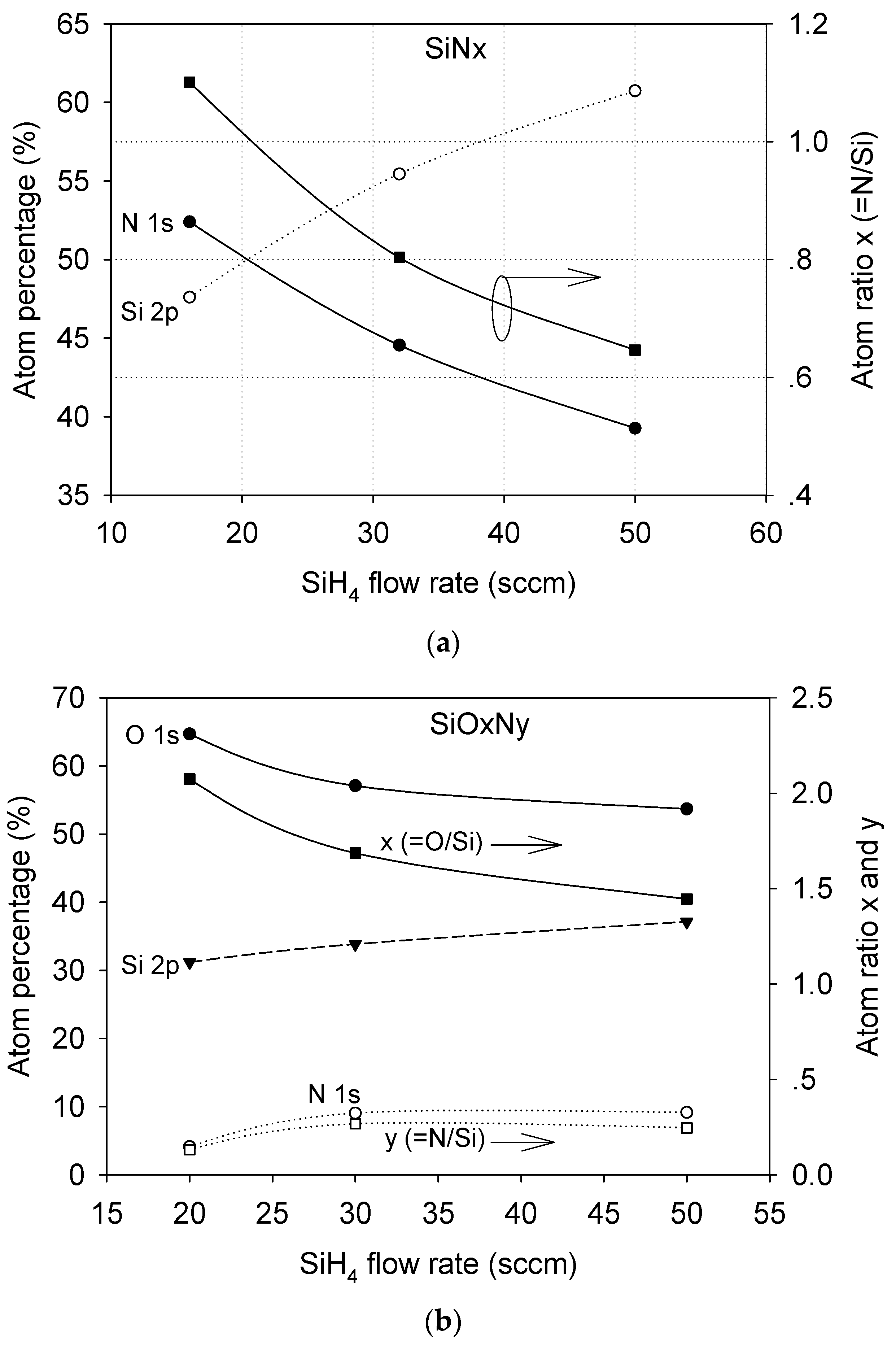
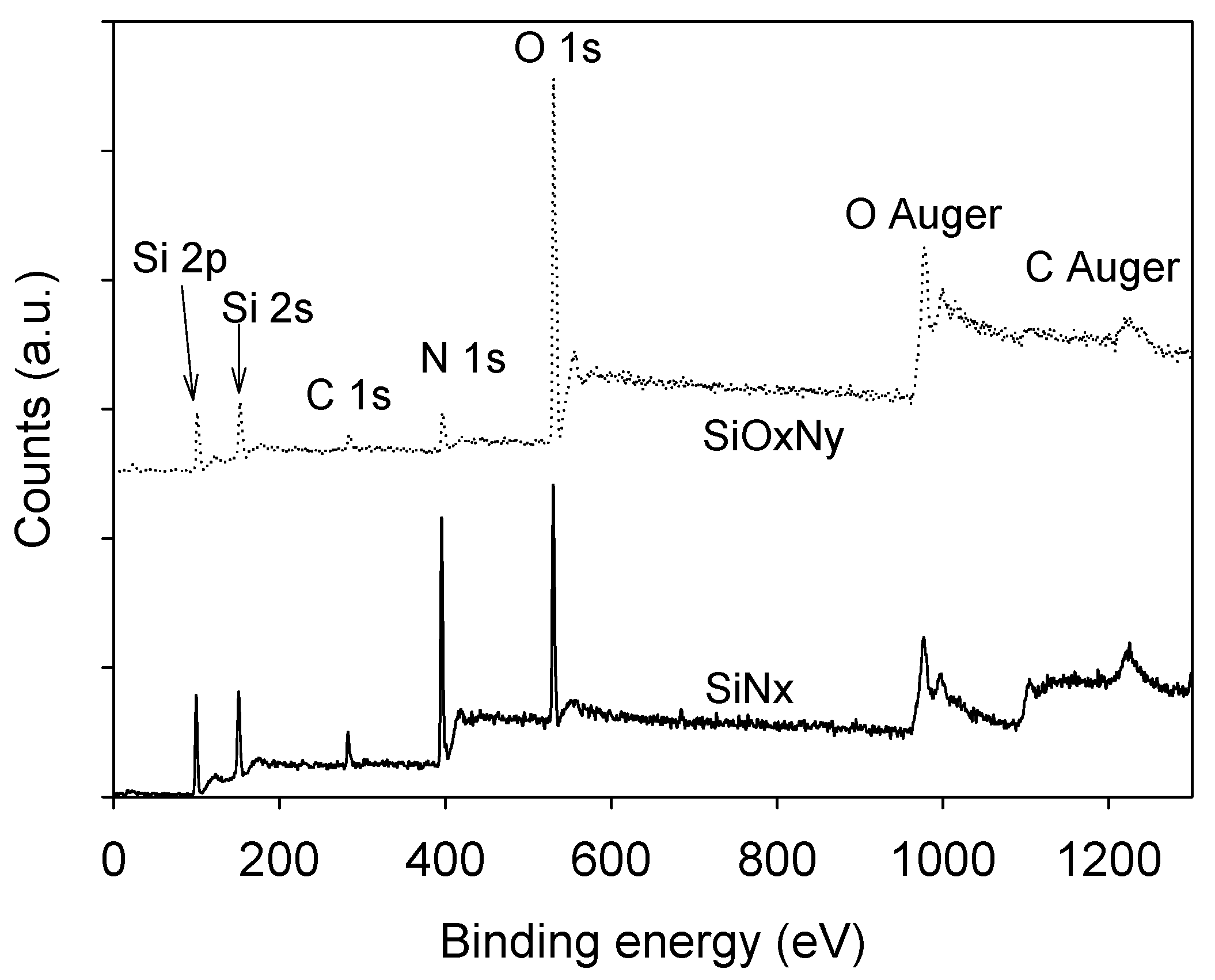
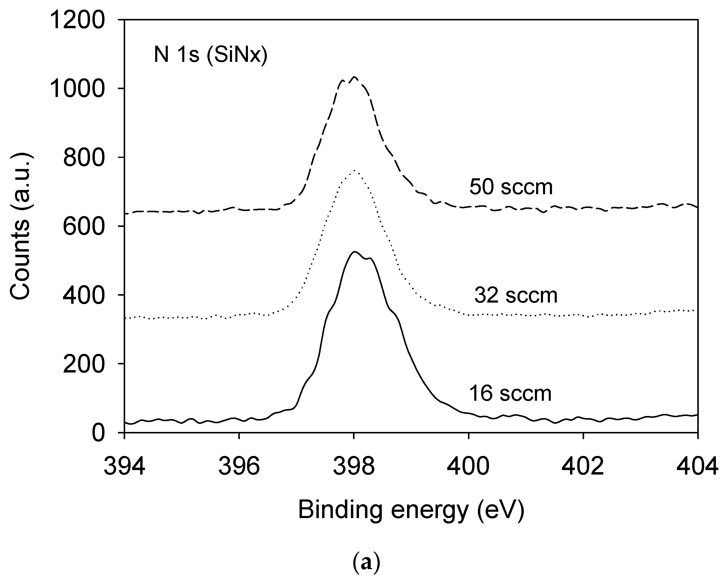
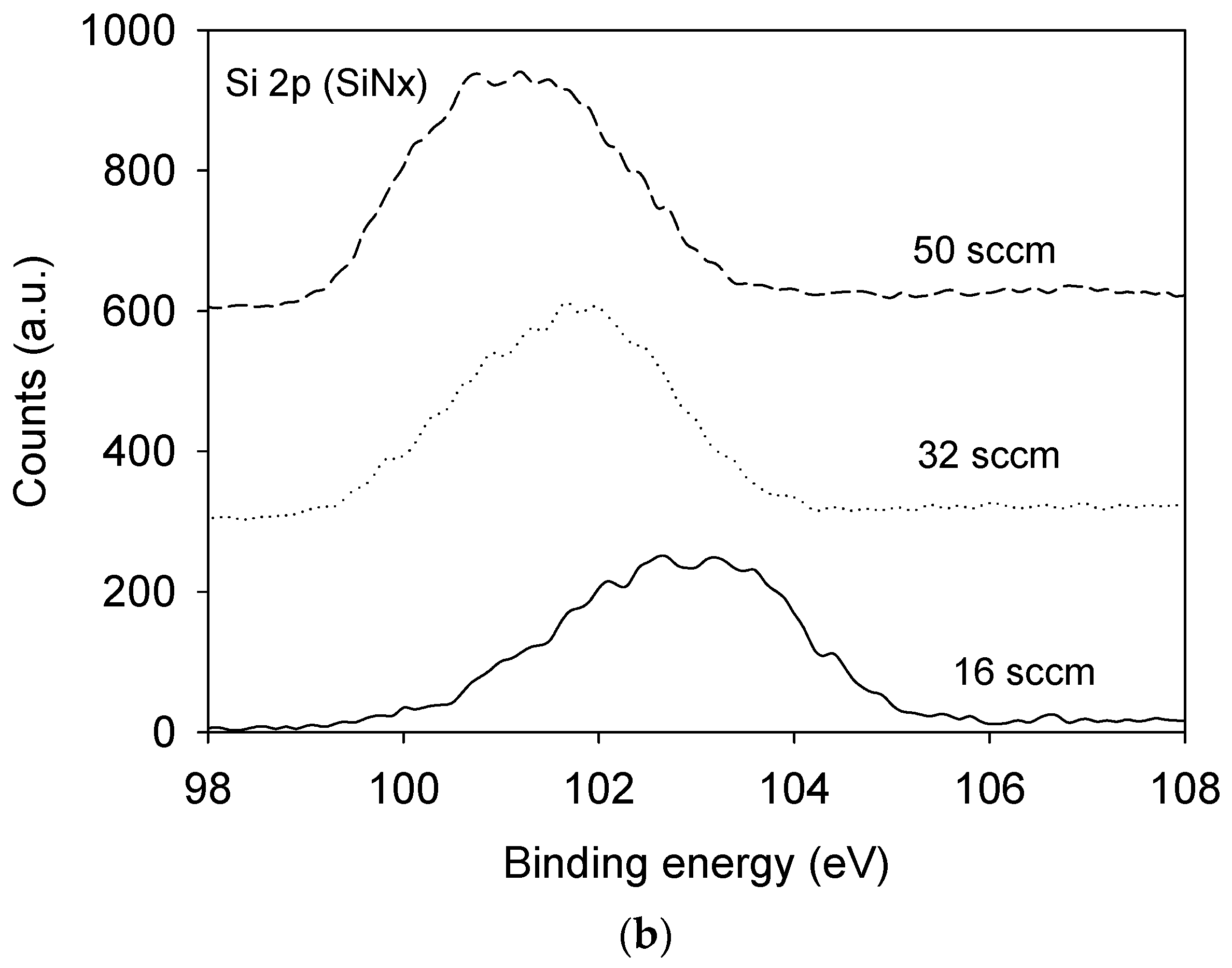
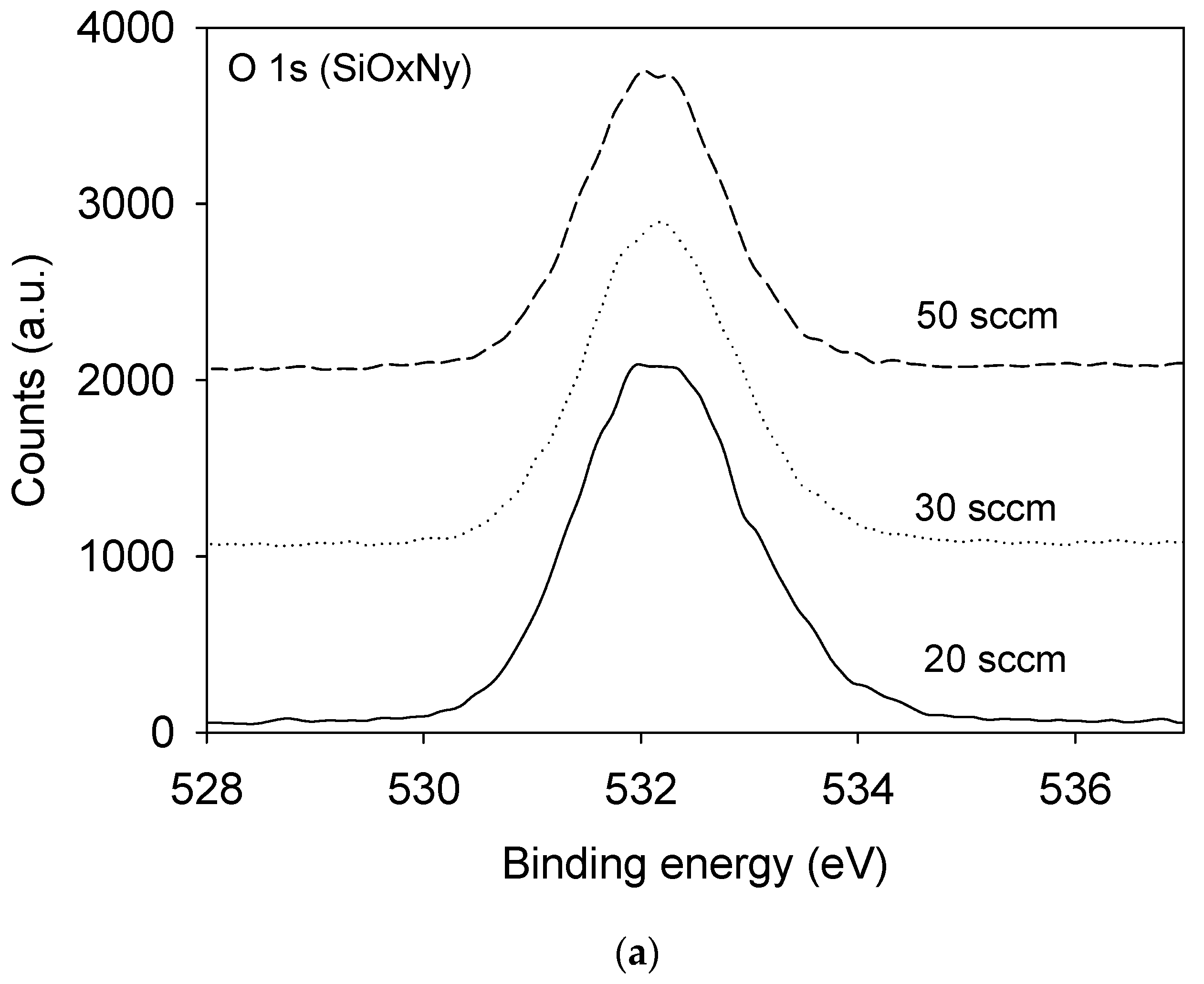
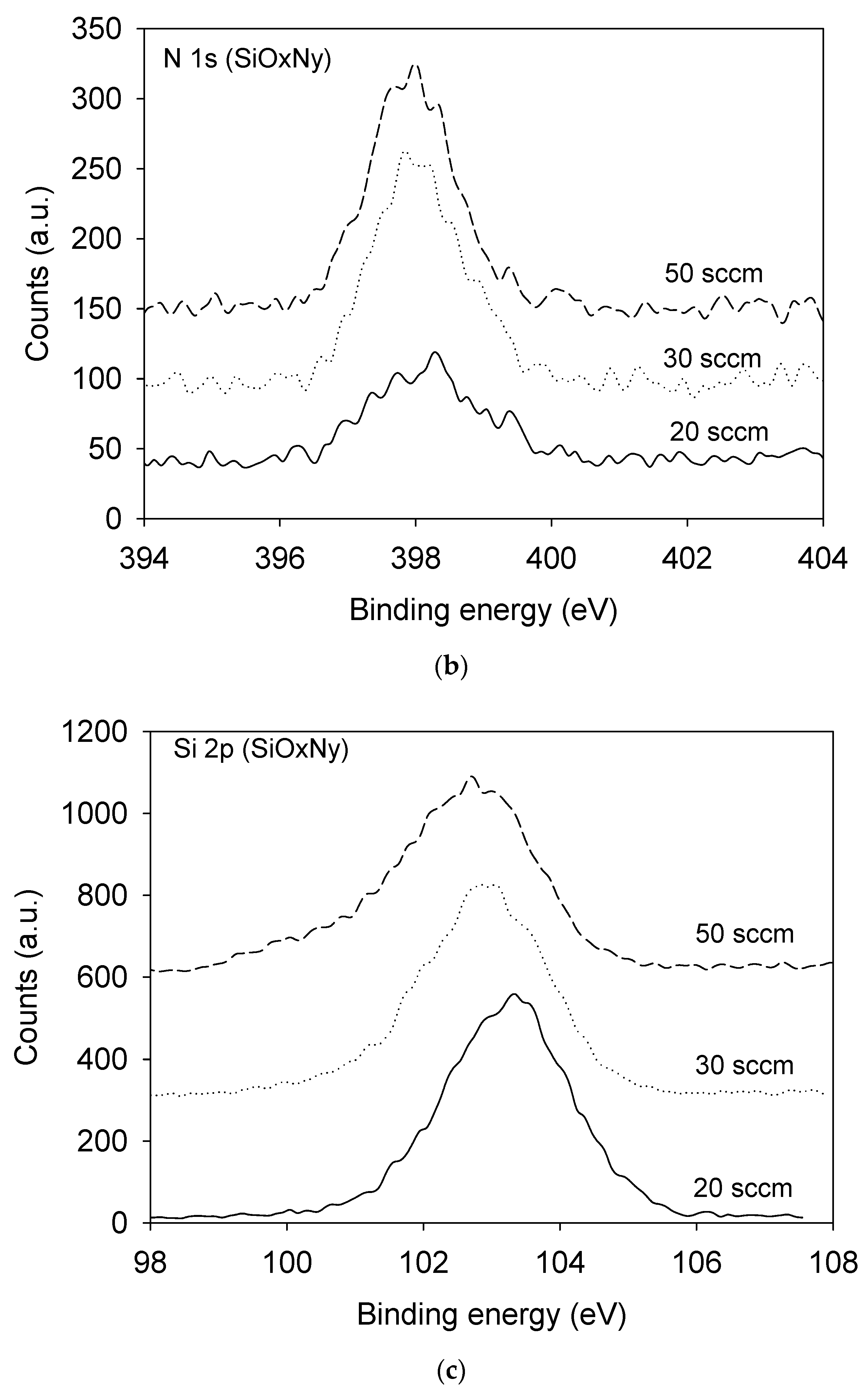
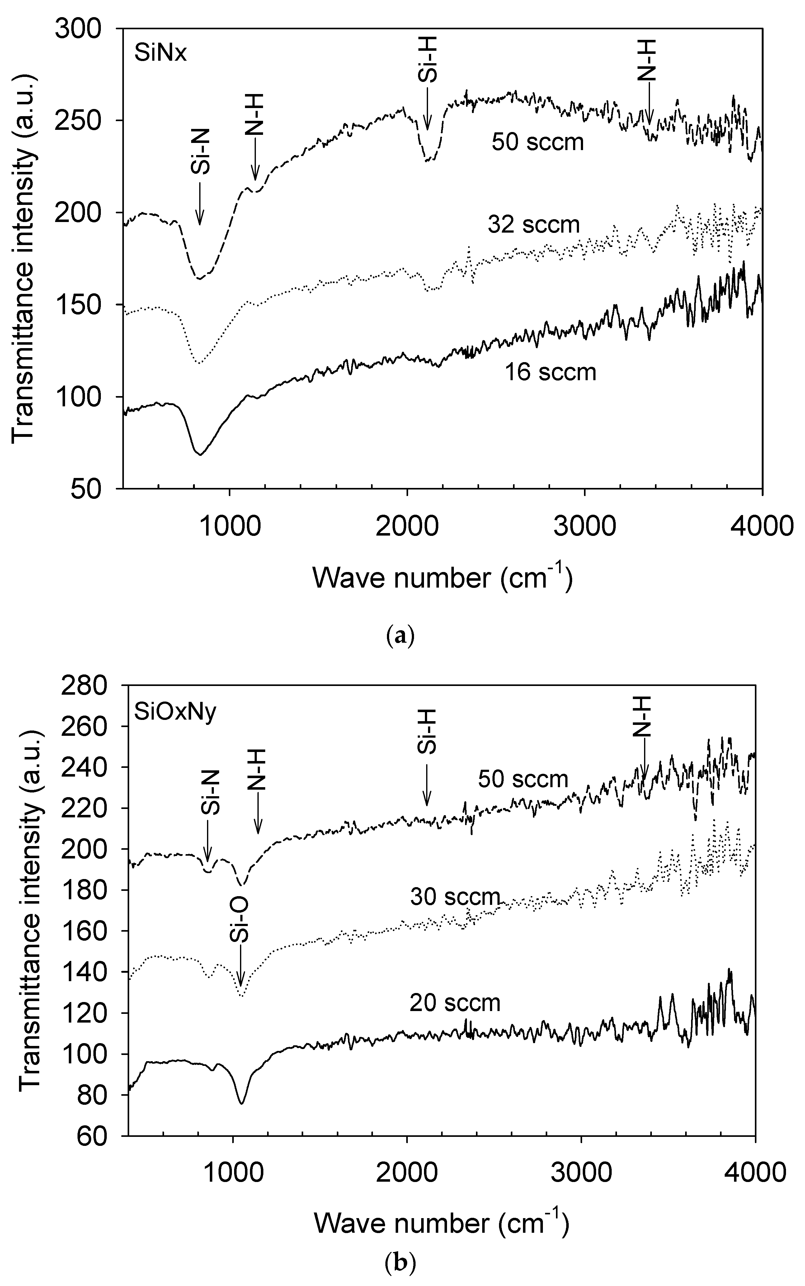
3.1. Film Composition and Bonding State Analysis

Figure 1 shows the atomic percentage and atomic ratio in the SiNx and SiOxNy films. The atomic percentages were average values for three independent sampling points, after surface etching for 4 min. In the SiNx films, it is clear that the Si concentration increased, and N concentration decreased with the increase of silane flow rate. The N:Si atomic ratio (Figure 1a) decreased from 1.1 to about 0.65 when the silane flow rate increased from 16 to 50 sccm.
In the SiOxNy films, the O atom concentration decreased, and the Si and N concentrations increased with the silane flow rate. In all cases, the O atomic concentration was always higher than 50%, the Si concentration was between 30% to 40%, and the N atom concentration was lower than 10%. As a result, the O:Si ratio was reduced from x = 2.07 to 1.45, while the N:Si ratio increased from y = 0.13 to 0.25.
Typical survey spectra of XPS for the surfaces of both SiNx and SiOxNy are presented in Figure 2, and they are globally similar to each other. The peaks corresponding to Si 2s and 2p, O 1s and Auger were clearly present. The N 1s peak was pronounced in the SiNx sample but was weak in the SiOxNy sample. A C 1s peak was also found, which was due to exposure of the samples to air after the film formation.
The high-resolution spectra of the SiNx sample corresponding to N 1s and Si 2p after etching are given in Figure 3a,b, respectively. They are plotted after the correction of charging effects using a binding energy of 284.6 eV, which was the C 1s peak obtained from the surface. It is noted that no peak of O 1s was detected after etching, although it was observed at the surface (Figure 2). It was seen that all the N 1s peaks were centered at 397.9 eV, which was attributed to the N-Si bond [23]. However, the relative height of the peak decreased with the increase of the silane flow rate. Figure 3b shows that the center of the Si 2p core level shifted from 102.8 eV to 101.7 eV and to 101 eV, corresponding to a silane flow rate of 16, 32, and 50 sccm, respectively. The binding energy shifted to a lower value, which was consistent with the decreasing of the N:Si ratio, as shown in Figure 1. A similar trend has also been confirmed by Hirohata et al. [23]. It was also observed that the relative height of the Si 2p peak increased with the increase of the silane flow rate because more Si atoms were incorporated into the films.
The high-resolution spectra of the SiOxNy sample corresponding to O 1s, N 1s, and Si 2p after etching are presented in Figure 4a–c. The O 1s and N 1s peaks were centered at 532.1 eV and 398 eV, respectively, which were not dependent on the silane flow rate. The centers of the Si 2p core level shifted to a lower binding energy. At the 20 sccm flow rate, the Si 2p peak was centered at 103.2 eV, which corresponded to the SiO2 bond. When the silane flow rate increased to 30 sccm and 50 sccm, the centers shifted to 102.7 eV and 102.6 eV, respectively. It was reported that the binding energy of silicon oxynitride depended on the nitrogen content [24]. The binding energy difference between silicon oxide and silicon oxynitride was between 1.5 and 3.9 eV. Thus, the current study finds that at the 20 sccm silane flow rate, the N concentration was so low that silicon dioxide (SiO2) predominantly formed. Silicon oxynitride became significant in samples with 30 and 50 sccm flow rates.
Figure 5 shows the FTIR spectra taken over a wavenumber range of 400–4000 cm−1 for both SiNx and SiOxNy films. The spectrum of the silicon substrate has already been subtracted. For SiNx films, the spectra revealed the Si–N bond with the characteristic stretching mode present near 810 cm−1. Other vibrations observed were N–H bending (approx. 1120 cm−1), Si–H stretching (approx. 2100 cm−1), and N–H stretching (approx. 3340 cm−1). These peaks were typical for low-temperature CVD silicon nitride films [25]. It was also observed that the absorptions corresponding to the vibrations of the N–H and Si–H bonds increased with increasing silane flow rate, indicating an increase in the hydrogen concentration. Hydrogen in the SiNx film is usually undesirable for microelectronic applications because it causes hydrogen-induced defects, which may reduce its insulating effect and induce large stress in the films at high temperature [26,27]. Therefore, lower flow rates of silane would be recommended in order to control the hydrogen content in the SiNx films.
For silicon oxynitride (SiOxNy) films, the absorption corresponding to the Si–O bond appeared at about 1020 cm−1 in all three cases (Figure 5b). The Si–N bond could also be observed at around 830 cm−1. It was clear that the absorption of the Si–N bond at the 20 sccm silane flow rate was very low, which was consistent with the low N content and the near-stoichiometric O:Si = 2 ratio, as indicated by XPS (Figure 1b). However, the absorption strength of Si–N increased with an increasing silane flow rate, demonstrating that more and more Si–N bonds were formed in the films. This result was consistent with the highest amount of nitrogen incorporated in the film at 50 sccm as indicated by XPS, and also agrees well with the formation of a silicon nitride phase in the film as characterized by XRD results shown later. It is worth mentioning that the lack of absorption at the N–H or Si–H locations indicated that the hydrogen concentration of these groups was less than 2–3 at%, or below the detection limit for the thin film IR spectroscopy [26,27]. Compared with the formation condition of SiNx films, the presence of oxygen during film formation has prevented Si–H and N–H bond formation.

3.2. Crystallinity and Phase Identification

Glancing angle X-ray diffraction patterns of the SiNx and SiOxNy films are shown in Figure 6a,b, respectively. The SiNx films were partly crystallized for all silane flow rates, as evidenced by all the broadened peaks. The XRD peaks belonged to neither α-Si3N4 nor β-Si3N4 [23]; rather, they seem to match better with the peaks of cubic silicon nitride (c-Si3N4) reported by Jiang et al. [28]. However, a cautionary note should be made that the cubic silicon nitride phase is usually prepared by a high-temperature and high-pressure process. Therefore, further work is needed to confirm the exact crystalline phase type and structure of our films. Since the atomic N:Si ratio was always lower than the stoichiometric ratio of 1.33, these nitride films did not seem to share a common equilibrium structure on deposition. For the SiOxNy shown in Figure 6b, it is clear that only amorphous phases were formed at both 20 sccm and 30 sccm flow rate. Combined with the XPS analysis reported earlier, the amorphous phase was predominantly SiO2 for the 20 sccm silane flow condition, and silicon oxynitride at 30 sccm. At a 50 sccm flow rate, similar XRD peaks to the silicon nitride films in Figure 6a were present, which meant the crystalline Si3N4 and amorphous oxynitride phase co-existed. This is justified by the XPS spectrum where the Si 2p core level binding energy at 50 sccm in the SiOxNy film further shifted to the SiNx side (Figure 4c).

3.3. Young’s Modulus and Hardness

Table 2 displays the Young’s modulus (E) and hardness (H) of both films. The Young’s moduli were calculated from the measured reduced moduli using nanoindentation. A typical load-displacement curve is shown in Figure 7. To carry out the calculation of the Young’s modulus of the film according to Equation (S2) (Supporting Information), the modulus and Poisson’s ratio for the diamond indenter tip, Edia = 1100 GPa and νdia = 0.2 were used. Poisson’s ratios for silicon nitride and silicon oxynitride films were taken as 0.27 and 0.23, respectively, based on References [29,30]. Overall, it was found that the hardness and Young modulus of SiNx films were greater than the ones of SiOxNy. Since the elasticity modulus is predominantly dependent on the bonding states, this finding agrees with the known fact that the Si–N bond is stiffer the Si–O bond.
The reported Young’s moduli for SiNx films were quite close to the ones obtained by Cardinale and Tustison [18], who found the biaxial modulus (which is E/(1 − ν)) of their PECVD silicon nitride films ranged from 110 to 160 GPa using a membrane bulge test. In general, the Young’s modulus obtained from PECVD SiNx films is lower than the one formed by low-pressure chemical deposition (LPCVD). The plane strain modulus (given by E/(1 − ν2)) of LPCVD was reported to be in the range of 230 to 330 GPa [31,32]. This is probably due to the higher synthesis temperatures used in LPCVD, typically at 700 °C or above. The obtained elastic modulus by LPCVD is closer to the sintered bulk Si3N4 (≈300 GPa). On the other hand, PECVD operates at low temperatures (100–300 °C), therefore the film density might be lower than the one created using high-temperature processes. Huang et al. [33] have recently found a correlation among deposition temperature, film density, and Young’s modulus in low-temperature PECVD silicon nitride films. In the current work, the Young’s modulus and hardness of SiNx was found to decrease with increasing silane flow rate, corresponding to a decreased atomic N:Si ratio in the film’s chemical composition. According Figure 1a, all the SiNx films were Si-rich (i.e., N:Si ratio less than 1.33), thus this work finds that the further away from the stoichiometric composition Si3N4, both the modulus and hardness decreased for the Si-rich nitride films. This implies that the elastic modulus of crystalline SiNx film was mainly controlled by the Si–N bonding. The slight decrease in the hardness with increasing silane flow may also be affected by the presence of an amorphous phase. However, in this work, we are not able to quantify the amount of amorphous phase in the films.
For silicon oxynitride films, Young’s modulus decreased slightly with increasing silane flow rate, and the variation is much smaller than for the SiNx series. It was noticed that the chemical composition (Si, N, O) only varied in a relatively narrow window. The values (89.2–76.8 GPa) were closer to silicon oxide (ESiO2 = 70 GPa) than silicon nitride, indicating dominance of the Si–O bond. This agrees with the XPS composition analysis in Figure 1b, which showed a low nitrogen concentration (4.1–9.2 at%) for the three samples. The obtained Young’s moduli for silicon oxynitride films fell in the range of 78–150 GPa, which was reported by other researchers [1,5,6,34].
The hardness of the SiOxNy films showed a great increase from 4.7 GPa to 9.7 GPa when the silane flow rate increased from 20 to 50 sccm. Unlike Young’s modulus, hardness is sensitive to both chemical bonding and microstructure. As analyzed earlier, at a 20 sccm flow rate, the film consisted of predominantly amorphous SiO2. This structure had the lowest hardness. When the flow rate increased to 30 sccm, the amorphous SiOxNy film had an increased hardness of 7.8 GPa. Although the composition was very close between the 30 sccm and 50 sccm films, only the 50 sccm sample contained a crystalline Si–N phase. The presence of a crystalline phase clearly contributed to the increase in hardness in the 50 sccm sample.

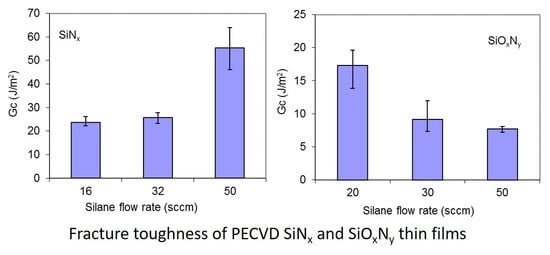
3.4. Fracture Toughness

Table 3 lists the critical energy release rate (GIc) and fracture toughness (KIC) for the SiNx and SiOxNy films. The GIc value obtained here is an intrinsic property of the films, which reflects a material’s ability to absorb energy for per unit-area crack growth. For easy compassion with literature data, which are mostly given in terms of the critical stress intensity factor, KIC, we have also converted the measured GIc into KIC following the relation: K Ic = G Ic E / ( 1 ν 2 ) . Typical values of the fracture toughness of steel, glass (amorphous silicon oxide), and a 200 nm-thick Si3N4 thin film are around 60, 0.6, and 1.8 MPa·m1/2, respectively [17]. The fracture toughness of our nitride and oxynitride films shown in Table 3 was close to the reported Si3N4 film.
The variation of the critical energy release rate with the silane flow rate is plotted in Figure 8. The GIc increased with increasing silane flow rate for the SiNx films, and an opposite trend was observed for the SiOxNy films. Such variations are in line with the trend of the film hardness: it is known that a harder material is likely to be more brittle (lower fracture energy). From the microstructure’s perspective, we attribute the greater fracture energy in the SiNx film with increasing silane flow rate to the increased amount of non-stoichiometric, Si-rich nitride phase in the films (and possibly increased amount of amorphous content). In the case of SiOxNy, the increased film brittleness with increasing silane flow rate was clearly related to the harder, crystalline silicon nitride phase as analyzed before.
From a mechanical point of view, SiNx films are preferred over SiOxNy films because the former possesses better material stiffness, hardness, and fracture toughness. As films dominated by ionic and covalent bonds are generally very brittle and prone to fracture when being used as structural elements in MEMS devices, having a greater fracture toughness is a clear advantage for the device reliability.

4. Conclusions

SiNx and SiOxNy thin films have been prepared using plasma enhanced chemical vapor deposition under varying silane flow rates. Film composition, chemical bonding, and microstructure were identified by X-ray photoelectron spectroscopy (XPS), Fourier transform infrared spectroscopy (FTIR), and X-ray diffraction (XRD). The Young’s modulus and hardness of the thin films were characterized using nanoindentation test. A controlled buckling test was used to measure the fracture toughness of these thin films. The current study found that the silicon nitride films had better overall mechanical properties than the silicon oxynitride thin films. The main reason was that the SiNx films were composed predominantly of the crystalline Si3N4 phase, while the SiOxNy films were dominated by the amorphous Si–O phase. Within the SiNx films, Young’s modulus and hardness decreased with increasing silane flow rate, corresponding to a reduced amount of the strong Si–N bonding. For the SiOxNy films, an increasing silane flow rate has shown a minor effect on the Young’s modulus but a significant impact on the hardness. The fracture toughness of both series of thin films displayed opposite trends with their hardness, and this could be explained by considering that the ability for energy dissipation increases with increased ductility (reduced hardness) of the materials. PECVD SiNx is preferred when structural components in MEMS are to be fabricated because of its better resistance to fracture.

Supplementary Materials

The following are available online at https://www.mdpi.com/2571-9637/1/1/6/s1.

Author Contributions

This work was initiated by Z.C. Experiment was carried out by Z.G., and analysis was done after discussion among all authors. Draft was prepared by Z.G., and revised by C.W. and Z.C.

Funding

This research was funded by The Ministry of Education, Singapore grant number RG 14/03.

Conflicts of Interest

The authors declare no conflict of interest.

References

  1. Jozwik, M.; Delobelle, P.; Gorecki, C.; Sabac, A.; Nieradko, L.; Meunier, C.; Munnik, F. Optomechanical characterization of compressively prestressed silicon oxynitride films deposited plasma-enhanced chemical vapour deposition on silicon membranes. Thin Solid Films 2004, 468, 84–92. [Google Scholar] [CrossRef]
  2. Prodanović, V.; Chan, H.W.; Graaf, H.V.D.; Sarro, P.M. Ultra-thin alumina and silicon nitride MEMS fabricated membranes for the electron multiplication. Nanotechnology 2018, 29, 155703. [Google Scholar] [CrossRef] [PubMed] [Green Version]
  3. Bagolini, A.; Savoia, A.S.; Picciotto, A.; Boscardin, M.; Bellutti, P.; Lamberti, N.; Caliano, G. PECVD low stress silicon nitride analysis and optimization for the fabrication of CMUT devices. J. Micromech. Microeng. 2015, 25, 015012. [Google Scholar] [CrossRef]
  4. Li, D.-L.; Feng, X.-F.; Wen, Z.-Y.; Shang, Z.-G.; She, Y. Stress control of silicon nitride films deposited by plasma enhanced chemical vapor deposition. Optoelectron. Lett. 2016, 12, 285–289. [Google Scholar] [CrossRef]
  5. Dong, J.; Du, P.; Zhang, X. Characterization of the Young’s modulus and residual stresses for a sputtered silicon oxynitride film using micro-structures. Thin Solid Films 2013, 545, 414–418. [Google Scholar] [CrossRef]
  6. Danaie, K.; Bosseboeuf, A.; Clerc, C.; Gousset, C.; Julie, G. Fabrication of UV-transparent SixOyNz membranes with a low frequency PECVD reactor. Sens. Actuators A 2002, 99, 78–81. [Google Scholar] [CrossRef]
  7. Jo, M.C.; Park, S.K.; Park, S.J. A study on resistance of PECVD silicon nitride thin film to thermal stress-induced cracking. Appl. Surf. Sci. 1999, 140, 12–18. [Google Scholar] [CrossRef]
  8. Yau, B.S.; Huang, J.L. Effects of nitrogen flow on R.F. reactive magnetron sputtered silicon nitride films on high speed steel. Surf. Coat. Technol. 2004, 176, 290–295. [Google Scholar] [CrossRef]
  9. Lane, M.W.; Liniger, E.G.; Lloyd, J.R. Relationship between interfacial adhesion and electromigration in Cu metallization. J. Appl. Phys. 2003, 93, 1417–1421. [Google Scholar] [CrossRef]
  10. Dauskardt, R.H.; Lane, M.; Ma, Q.; Krishna, N. Adhesion and debonding of multi-layer thin film structures. Eng. Fract. Mech. 1998, 61, 141–162. [Google Scholar] [CrossRef]
  11. Skjöldebrand, C.; Schmidt, S.; Vuong, V.; Pettersson, M.; Grandfield, K.; Högberg, H.; Engqvist, H.; Persson, C. Influence of Substrate Heating and Nitrogen Flow on the Composition, Morphological and Mechanical Properties of SiNx Coatings Aimed for Joint Replacements. Materials 2017, 10, 173. [Google Scholar] [CrossRef] [PubMed]
  12. Obrosov, A.; Gulyaev, R.; Zak, A.; Ratzke, M.; Naveed, M.; Dudzinski, W.; Weiß, S. Chemical and Morphological Characterization of Magnetron Sputtered at Different Bias Voltages Cr-Al-C Coatings. Materials 2017, 10, 156. [Google Scholar] [CrossRef] [PubMed]
  13. Sajgalik, P.; Dusza, J.; Hoffmann, M.J. Relationshop between microstructure, toughening mechanisms, and fracture toughness of reinforced silicon nitride ceramics. J. Am. Ceram. Soc. 1995, 78, 2619–2624. [Google Scholar] [CrossRef]
  14. Becher, P.F.; Sun, E.Y.; Plucknett, K.P.; Alexander, K.B.; Hsueh, C.-H.; Lin, H.-T.; Waters, S.B.; Westmoreland, C.G.; Kang, E.; Hirao, K.; et al. Microstructural design of silicon nitride with imporved fracture toughness: I, effects of grain shape and size. J. Am. Ceram. Soc. 1998, 81, 2821–2830. [Google Scholar] [CrossRef]
  15. Doblinger, M.; Winkelman, G.G.; Dwyer, C.; Marsh, C.; Kirkland, A.I.; Cockayne, D.J.H.; Hoffmann, M.J. Structural and compositional comparison of Si3N4 ceramics with different fracture modes. Acta Mater. 2006, 54, 1949–1956. [Google Scholar] [CrossRef]
  16. Satet, R.L.; Hoffmann, M.J. Influence of the rare-earth element on the mechanical properties of RE-Mg-bearing silicon nitride. J. Am. Ceram. Soc. 2005, 88, 2485–2490. [Google Scholar] [CrossRef]
  17. Fan, L.S.; Howe, R.T.; Muller, R.S. Fracture toughness characterization of brittle thin films. Sens. Actuators 1990, A21–A23, 872–874. [Google Scholar] [CrossRef]
  18. Cardinale, G.F.; Tustison, R.W. Fracture strength and biaxial modulus measurement of plasma silicon nitride films. Thin Solid Films 1992, 207, 126–130. [Google Scholar] [CrossRef]
  19. Chen, Z.; Cotterell, B.; Wang, W.; Guenther, E.; Chua, S.J. A mechanical assessment of flexible optoelectronic devices. Thin Solid Films 2001, 394, 202–206. [Google Scholar] [CrossRef]
  20. Chen, Z.; Cotterell, B.; Wang, W. The Fracture of Brittle Thin Films on Compliant Substrate in Flexible Displays. Eng. Fract. Mech. 2002, 69, 597–603. [Google Scholar] [CrossRef]
  21. Chen, Z.; Gan, Z.H. Fracture Toughness Measurement of Thin Films on Compliant Substrate Using Controlled Buckling Test. Thin Solid Films 2007, 515, 3305–3309. [Google Scholar] [CrossRef]
  22. Chen, Z.; Xu, X.; Wong, C.C.; Mhaisalkar, S. Effect of Plating Parameters on the Intrinsic Stress in Electroless Nickel Plating. Surf. Coat. Technol. 2003, 167, 170–176. [Google Scholar] [CrossRef]
  23. Hirohata, Y.; Shimamoto, N.; Hino, T.; Yamashima, T.; Yabe, K. Properties of silicon nitride films prepared by magnetron sputtering. Thin Solid Films 1994, 253, 425–429. [Google Scholar] [CrossRef]
  24. Mao, A.Y.; Son, K.A.; Hess, D.A.; Brown, L.A.; White, J.M.; Kwong, D.L.; Roberts, D.A.; Vrtis, R.N. Annealing ultra thin Ta2O5 films deposited on bare and nitrogen passivated Si(100). Thin Solid Films 1999, 349, 230–237. [Google Scholar] [CrossRef]
  25. Tolstoy, V.P.; Chernyshova, I.V.; Skryshevsky, V.A. Infrared spectroscopy of thin layers in silicon microelectronics. In Handbook of Infrared Spectroscopy of Ultrathin Films; John Wiley & Sons: Hoboken, NJ, USA, 2003; pp. 435–436. [Google Scholar]
  26. Gupta, M.; Rathi, V.K.; Thangaraj, R.; Agnihotri, O.P.; Chari, K.S. Preparation, properties and applications of silicon nitride thin films deposited by plasma-enhanced chemical vapor deposition. Thin Solid Films 1991, 204, 77–106. [Google Scholar] [CrossRef]
  27. Han, S.S.; Jun, B.H.; No, K.; Bae, B.S. Preparation of a-SiNx thin film with low hydrogen content by inductively coupled plasma enhanced chemical vapor deposition. J. Electrochem. Soc. 1998, 145, 652–658. [Google Scholar] [CrossRef]
  28. Jiang, J.Z.; Lindelov, H.; Gerward, L.; Stahl, K.; Recio, J.M.; Mori-Sanchez, P.; Carlson, S.; Mezouar, M.; Dooryhee, E.; Fitch, A.; et al. Compressibility and thermal expansion of cubic silicon nitride. Phys. Rev. B 2002, 65, 161202(R). [Google Scholar] [CrossRef]
  29. Lynch, C.T. (Ed.) CRC Handbook of Materials Science; CRC Press: Boca Raton, FL, USA, 1975; Volume II. [Google Scholar]
  30. Carlotti, G.; Colpani, P.; Piccolo, D.; Santucci, S.; Senez, V.; Socino, G.; Verdini, L. Measurement of the elastic and viscoelastic properties of dielectric films used in microelectronics. Thin Solid Films 2002, 414, 99–104. [Google Scholar] [CrossRef]
  31. Hong, S.; Weihs, T.P.; Bravman, J.C.; Nix, W.D. Measuring stiffness and residual stresses of silicon nitride thin films. J. Electron. Mater. 1990, 19, 903–910. [Google Scholar] [CrossRef]
  32. Toivola, Y.; Thurn, J.; Cook, R.F.; Cibuzar, G.; Roberts, K. Influence of deposition conditions on mechanical properties of low-pressure chemical vapor deposited low-stress silicon nitride films. J. Appl. Phys. 2003, 94, 6915–6922. [Google Scholar] [CrossRef]
  33. Huang, H.; Winchester, K.J.; Suvorova, A.; Lawn, B.R.; Liu, Y.; Hu, X.Z.; Dell, J.M.; Faraone, L. Effect of deposition conditions on mechanical properties of low-temperature PECVD silicon nitride films. Mater. Sci. Eng. A 2006, 435–436, 453–459. [Google Scholar] [CrossRef]
  34. Kramer, T.; Paul, O. Postbuckled micromachined square membranes under differential pressure. J. Micromech. Microeng. 2003, 12, 475–478. [Google Scholar] [CrossRef]
Figure 1. Atomic percentage and atomic ratio in the (a) SiNx and (b) SiOxNy films.
Surfaces 01 00006 g001
Figure 2. Typical survey spectra of XPS for surfaces of both SiNx and SiOxNy films.
Surfaces 01 00006 g002
Figure 3. The high-resolution spectra of the SiNx samples corresponding to (a) N 1s and (b) Si 2p after etching. Films were formed using varied silane flow rates of 16, 32, and 50 sccm.
Surfaces 01 00006 g003aSurfaces 01 00006 g003b
Figure 4. The high-resolution spectra of the SiOxNy sample corresponding to (a) O 1s, (b) N 1s, and (c) Si 2p after etching. Three films with varied silane flow rate are shown.
Surfaces 01 00006 g004aSurfaces 01 00006 g004b
Figure 5. FTIR spectra taken over a wavenumber range of 400–4000 cm−1 for (a) SiNx and (b) SiOxNy films.
Surfaces 01 00006 g005
Figure 6. Glancing angle x-ray diffraction patterns of the (a) SiNx and (b) SiOxNy films at different silane flow rates.
Surfaces 01 00006 g006
Figure 7. A load-displacement curve during a nanoindentation test.
Surfaces 01 00006 g007
Figure 8. Critical energy release rate (GIc) for the (a) SiNx and (b) SiOxNy films with variation of the silane flow rate.
Surfaces 01 00006 g008
Table 1. Deposition parameters of PECVD silicon nitride and oxynitride films.
FilmSiH4 Flow Rate (sccm)N2O Flow Rate (sccm)NH3 Flow Rate (sccm)Pressure (mTorr)Radio Frequency Power (W)
SiOxNy20, 30, 50400--730100
SiNx16, 32, 50--160620250
Table 2. Young’s modulus and hardness obtained by nanoindentation.
FilmSilane Flow Rate (sccm)Young’s Modulus (GPa)Hardness (GPa)Poisson’s Ratio [27,28]
SiNx16153.0 ± 14.913.6 ± 2.90.27
32117.8 ± 9.511.8 ± 1.8
50108.5 ± 10.610.2 ± 3.0
SiOxNy2089.2 ± 4.84.7 ± 0.70.23
3078.9 ± 12.67.8 ± 0.9
5076.8 ± 9.69.7 ± 4.0
Table 3. The critical energy release rate (GIC) and fracture toughness (KIc) of SiNx and SiOxNy films.
FilmSilane Flow Rate (sccm)Film Thickness (nm)Fracture Strain (%)GIC (J/m2)KIC (MPa⋅m1/2)
SiNx16223.40.94823.731.90
32283.21.16725.661.74
50358.51.36755.412.44
SiOxNy20198.91.49717.291.24
30245.61.0729.160.85
50227.91.0467.690.77

