Article

Infrared and Terahertz Spectra of Sn-Doped Vanadium Dioxide Films

1
Tydex LLC, 194292 Saint Petersburg, Russia
2
Department of Chemistry, Lomonosov Moscow State University, 119991 Moscow, Russia
3
Department of Materials Science, Lomonosov Moscow State University, 119991 Moscow, Russia
4
Kurnakov Insitute of General and Inorganic Chemistry RAS, 119991 Moscow, Russia
*
Author to whom correspondence should be addressed.
Ceramics 2023, 6(2), 1291-1301; https://doi.org/10.3390/ceramics6020079
Submission received: 26 May 2023 / Revised: 10 June 2023 / Accepted: 13 June 2023 / Published: 15 June 2023
(This article belongs to the Special Issue Advanced Glasses and Glass-Ceramics)

Abstract

:
This work reports the effect of tin (Sn) doping on the infrared (IR) and terahertz (THz) properties of vanadium dioxide (VO 2 ) films. The films were grown by hydrothermal synthesis with a post-annealing process and then fully characterized by X-ray diffraction (XRD), Raman spectroscopy, scanning electron microscopy (SEM), and temperature-controlled electrical resistivity as well as IR and THz spectroscopy techniques. Utilizing (NH 4 ) 2 SnF 6 as a Sn precursor allows the preparation of homogeneous Sn-doped VO 2 films. Doping of VO 2 films with Sn led to an increase in the thermal hysteresis width while conserving the high modulation depth in the mid-IR regime, which would be beneficial for the applications of VO 2 films in IR memory devices. A further analysis shows that Sn doping of VO 2 films significantly affects the temperature-dependent THz optical properties, in particular leading to the suppression of the temperature-driven THz transmission modulation. These results indicate Sn-doped VO 2 films as a promising material for the development of switchable IR/THz dichroic components.

1. Introduction

The mid-infrared (2–20 µm wavelength range) spectral region attracts attention from both scientific and industrial sectors due to the availability of multiple atmospheric windows and its technological potential in thermal imaging [1], free space communications [2], and chemical and biological molecular sensing [3,4] because of the fingerprint vibrational and rotational motions of molecules within this spectral region. Full utilization of mid-infrared radiation’s potential still requires active optical components. Phase change materials such as best known as vanadium dioxide (VO 2 ) can also be useful for the development of mid-infrared photonic applications, especially when combined with resonant plasmonic structures. In recent years, VO 2 has been widely used as the basis of active metamaterials operating in the mid-infrared range [5,6,7,8,9,10,11].
VO 2 -based devices’ functional performance significantly depends on the morphology, preparation methods, and doping of VO 2 films [12]. The most remarkable property of VO 2 is the multi-stimulus-induced [13] reversible phase transition from a dielectric to a metallic state [14]. This metal–insulator transition (MIT) leads to an abrupt variation in its electric, thermal, and optical properties [15]. There are four main criteria defining the performance of the MIT in VO 2 : the phase transition amplitude, the phase transition sharpness, the hysteresis width, and the state stability before and after phase transition. Element doping enables tailoring of these key VO 2 performances for application requirements [16].
The temperature of the MIT can be decreased by doping with high valance metal ions (W 6 + , Mo 6 + , and Nb 5 + ) [17,18,19] or increased by doping with low valence atoms (Fe) [20] from its initial value for undoped VO 2 of 68 C according to the application requirements. Since the phase transition points for cooling and heating processes are incompatible, this results in thermal hysteresis ( Δ T MIT ). The thermal hysteresis width can be reduced by doping with titanium [21], niobium [22], and tungsten [23] or increased by doping with boron [23]. The phase transition sharpness is defined as the full width at half maximum (FWHM) of the Gaussian fitted differential d ( T r ) / d ( T ) versus temperature curves. Commonly, VO 2 element doping reduces the phase transition sharpness [24,25], except for doping with SiO 2 [26].
It was reported that Sn-doped VO 2 films fabricated by hydrothermal synthesis with SnCl 4 ·5H 2 O as the tin precursor possess an enhanced visible light transmittance [27]. W-Sn co-doped VO 2 films exhibit an improved visible transmittance with a reduced MIT temperature [28].
A dichroic optical component can provide the ability to manipulate radiation differently concerning its frequency band [29,30]. Among the dichroic elements demonstrated thus far, conductive thin films such as indium tin oxide [31,32,33] and La-doped BaSnO 3 [34] have been utilized in near-infrared transparent/terahertz functional devices. However, infrared functional devices with a high terahertz transparency still need to be explored.
In this paper, the potential of Sn-doped VO 2 films prepared by hydrothermal synthesis and a post-annealing process in temperature-driven mid-infrared and terahertz optical modulation is determined. To reveal the effect of the VO 2 dopant on the optical properties in the mid-IR spectral range across the MIT, the Sn doping levels were varied. Given the high modulation depth and increased thermal hysteresis width in the mid-IR range, we envision the application of Sn-doped VO 2 films for adaptive infrared camouflage and optical memory-type devices. Moreover, the revealed temperature-dependent modulation suppression in the THz range is helpful for the development of dichroic optical elements.

2. Experimental Details

2.1. Preparation of Sn-Doped VO 2 Samples

Sn-doped VO 2 films were deposited on 0.5 mm single crystal r-cut sapphires substrates polished on one-side (r-Al 2 O 3 Monocrystal Co., Ltd., Stavropol, Russia) by hydrothermal synthesis [35]. Vanadium precursors were synthesized using vanadium pentoxide (V 2 O 5 ) and oxalic acid (H 2 C 2 O 4 ·2H 2 O) as starting materials. A mixture of ethylene glycol (EG) and deionized (DI) water was selected as a solvent. Sn-doped vanadium dioxide was obtained by adding hexafluorostannate ((NH 4 ) 2 SnF 6 ) as a doping agent.
For producing an aqueous V 4 + -containing solution, V 2 O 5 and H 2 C 2 O 4 ·2H 2 O were mixed in a molar ratio of 1:3 in DI water with continuous magnetic stirring for 6 h at 80 °C. Thereafter, the required amount of EG (DI water/EG = 1:1 V / V ) was added. The calculated amount of (NH 4 ) 2 SnF 6 was dissolved in a DI/EG solution of V 4 + . As a result, a precursor solution with different concentrations of tin was obtained. Concentrations of 1% and 1.5% of tin were chosen for the synthesis. This precursor was diluted with the DI/EG solvent to obtain a V 4 + cation concentration of 3.125 mmol/L.
Sn-doped VO 2 (M 1 ) films on r-Al 2 O 3 substrates were synthesized with hydrothermal deposition with a post-annealing process. Prior to deposition, r-Al 2 O 3 crystals (0.55 × 1.5 cm 2 ) were cleaned with DI water and acetone. Then, the substrates were placed into a high-density 25 mL polyparaphenol (PPL)-lined hydrothermal synthesis autoclave reactor in a vertical position using a Teflon holder. Thereafter, the precursor solution was transferred into the PPL cup with a filling ratio of 0.60 and sealed hermetically in a stainless autoclave. The autoclave was kept at 180 °C for 20 h and then cooled down to room temperature naturally. The films deposited on the substrates were cleaned with DI water and acetone several times and dried for 30 min at room temperature. Post-annealing was performed in an argon gas atmosphere (3 mbar, Ar flow (3.5 L/h)) in two steps. The first step at 400 °C for 30 min was intended to remove any EG residues. On the second annealing, the temperature was increased to 600 °C for 60 min.
Based on the Sn concentration, the samples were denoted as S0 (undoped VO 2 ), S1 (1% Sn), and S2 (1.5% Sn).

2.2. Characterization Studies

The phase purity and crystallinity of VO 2 films were analyzed by X-ray diffraction (XRD, Rigaku SmartLab) with Cu K α ( λ = 1.54046 Å). The diffraction data were recorded in the 2 θ range of 20–80° with a resolution of 0.02° at a speed of 5 °/min. The surface morphology of the films and their thickness were characterized by scanning electron microscopy (SEM) using a Carl Zeiss NVision 40 electron microscope. Raman scattering measurements were performed using a Renishaw InVia spectrometer with a 514 nm 20 mW defocused excitation laser source (20 μ m spot) at room temperature. The electrical properties of the films were measured with a standard four-probe method in the temperature range of 25–90 °C using a Keithley 2700 multimeter. The temperature-dependent infrared transmittance in the wavelength range of 1.5–8 μ m was investigated using a Bruker Vertex 70 Fourier spectrometer. Finally, the terahertz transmission in the frequency range of 0.1–1 THz was measured using a Menlo Systems TERA K8 terahertz time-domain (THz-TDS) spectroscopy system. All the temperature-dependent optical characterizations were performed with a Peltier-based homemade temperature control system.

3. Results and Discussion

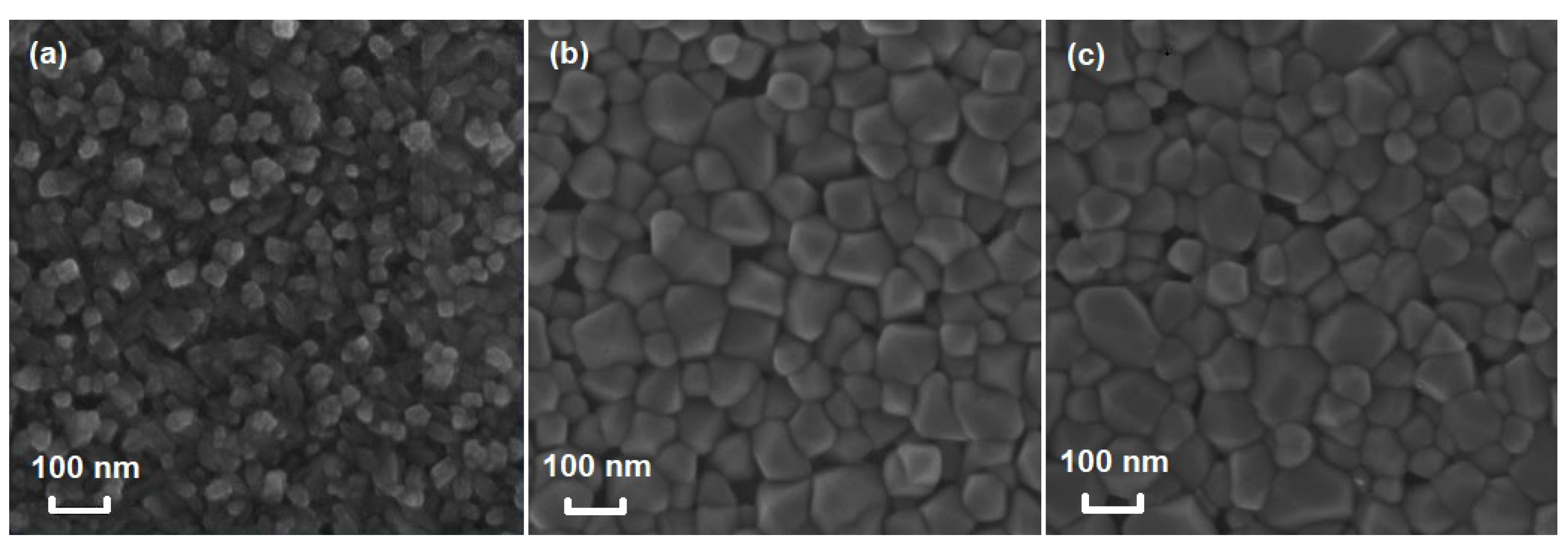
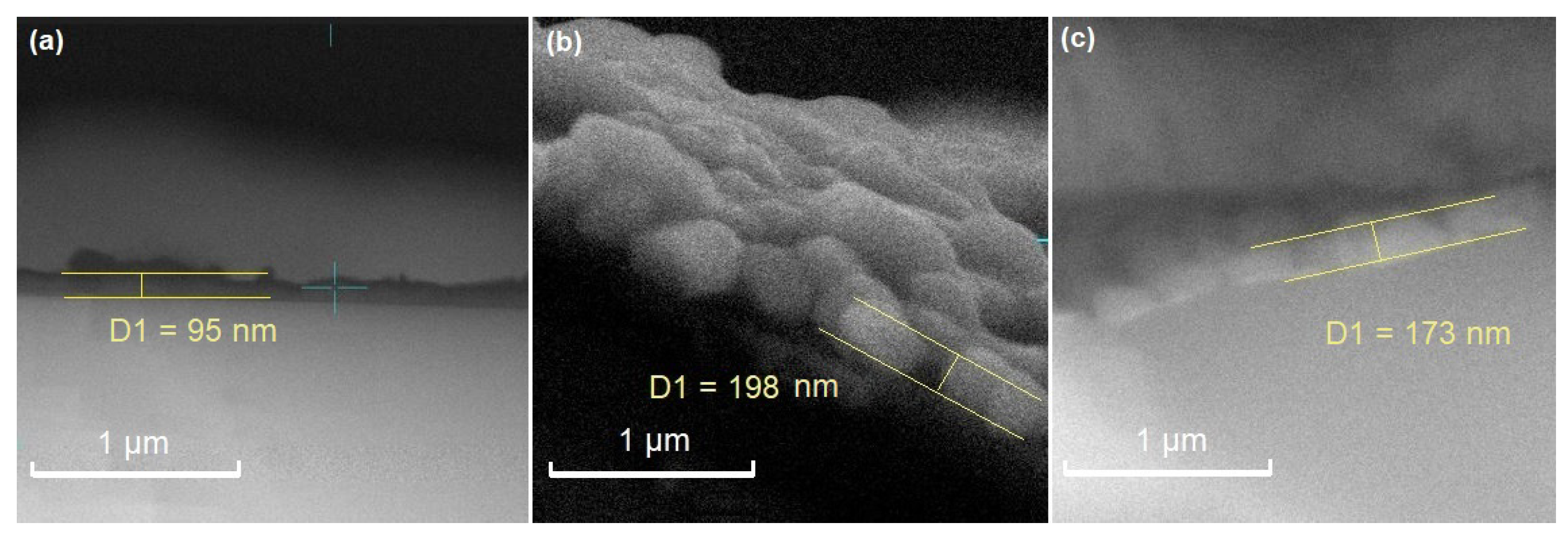
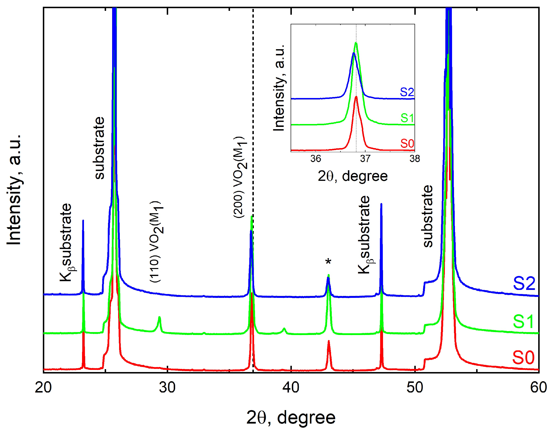
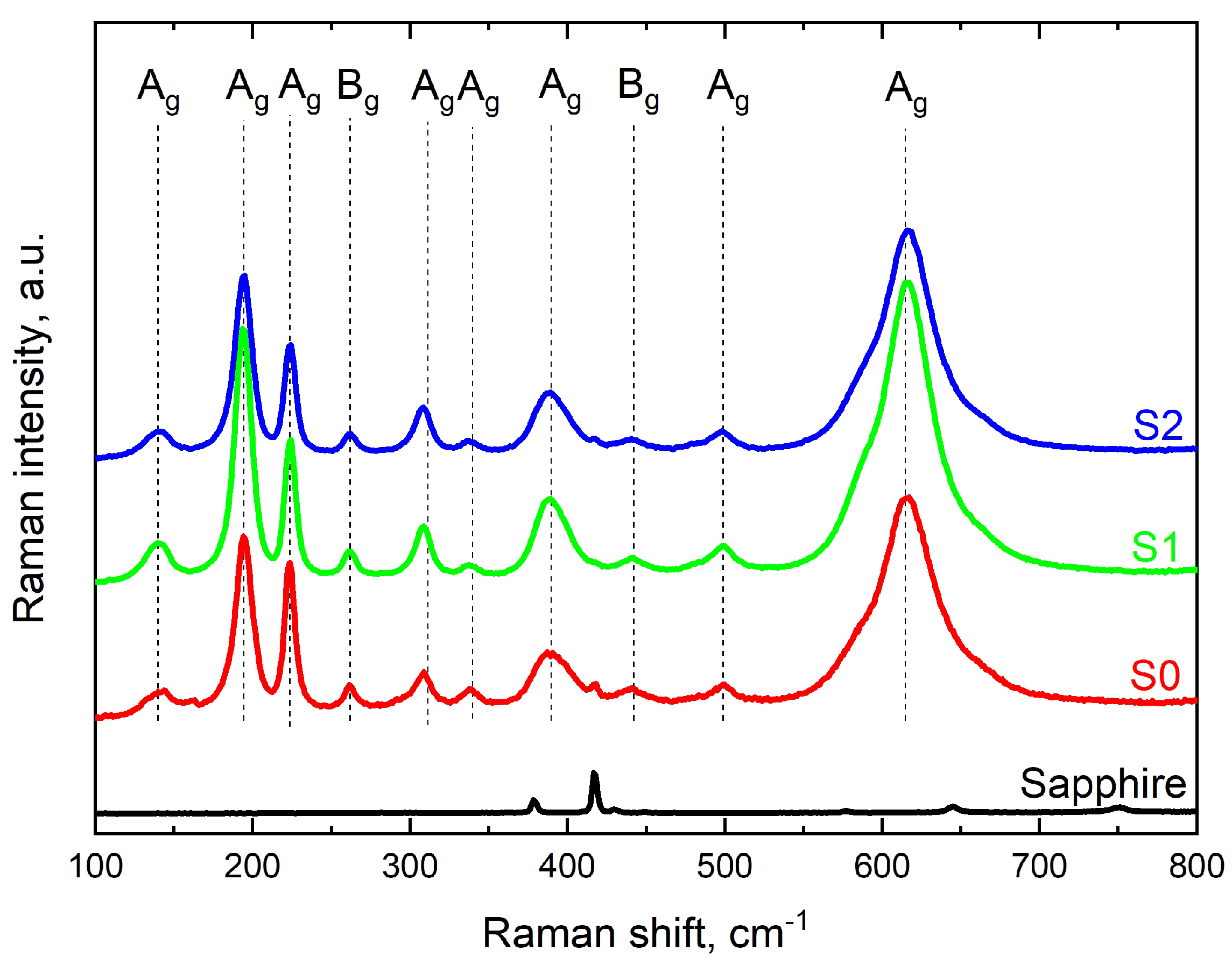
3.1. Structural and Morphological Analysis

Figure 1 shows surface morphology SEM images of Sn-doped VO 2 films with different Sn contents. Doped and undoped VO 2 films exhibited uniform homogeneous coverage of the substrate with quasi-spherical grains. Doping with Sn (Figure 1b,c) led to a significant increase in the quasi-spherical grain size, while various doping levels had a minor effect on film morphology.
The SEM cross-sectional images shown in Figure 2 indicate that VO 2 doping with Sn leads to an increase in film thickness. All the doped films have a thickness lying in the range of 170–200 nm, while the undoped VO 2 film is 95 nm thick.
The crystalline structures of Sn-doped VO 2 films on sapphire substrates were analyzed by XRD measurements at room temperature as shown in Figure 3.
The XRD results show that no additional phase appears in the XRD pattern after Sn doping. All obtained films are polycrystalline or 200 textured. The diffraction peaks are typical of VO 2 (M), ICDD PDF#43-1051. This indicates that doping with Sn does not significantly change the lattice constants of VO 2 films. However, the XRD peak with an angular position of 36.9° corresponding to the (200) VO 2 (M1) crystalline plane slightly shifts towards a lower angle with an increase in the Sn dopant.
The typical Raman signature of monoclinic VO 2 (M1) was obtained for undoped and Sn-doped VO 2 samples (Figure 4).
Raman scattering peaks position were identified at 143 (A g ), 195 (A g ), 224 (B g ), 262 (B g ), 309 (A g ), 340 (A g ), 391 (A g ), 442 (B g ), 499 (A g ), and 614 (A g ) cm 1 , which clearly conforms with the typical pattern [36].

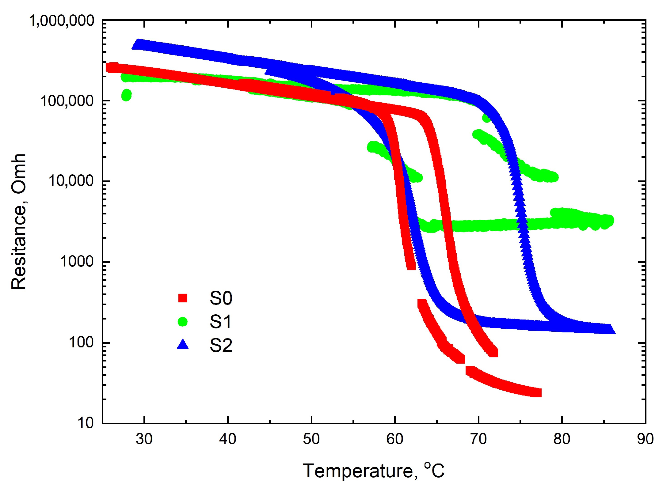
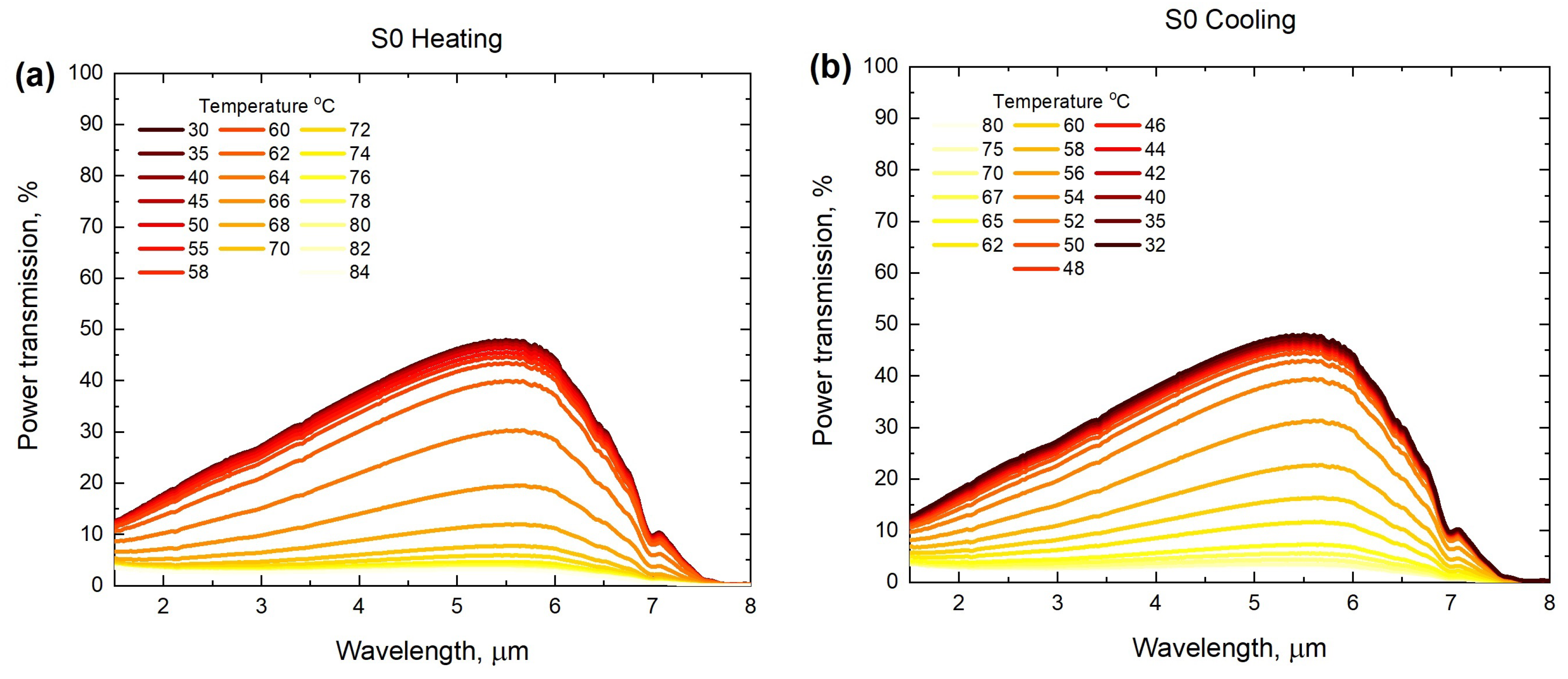
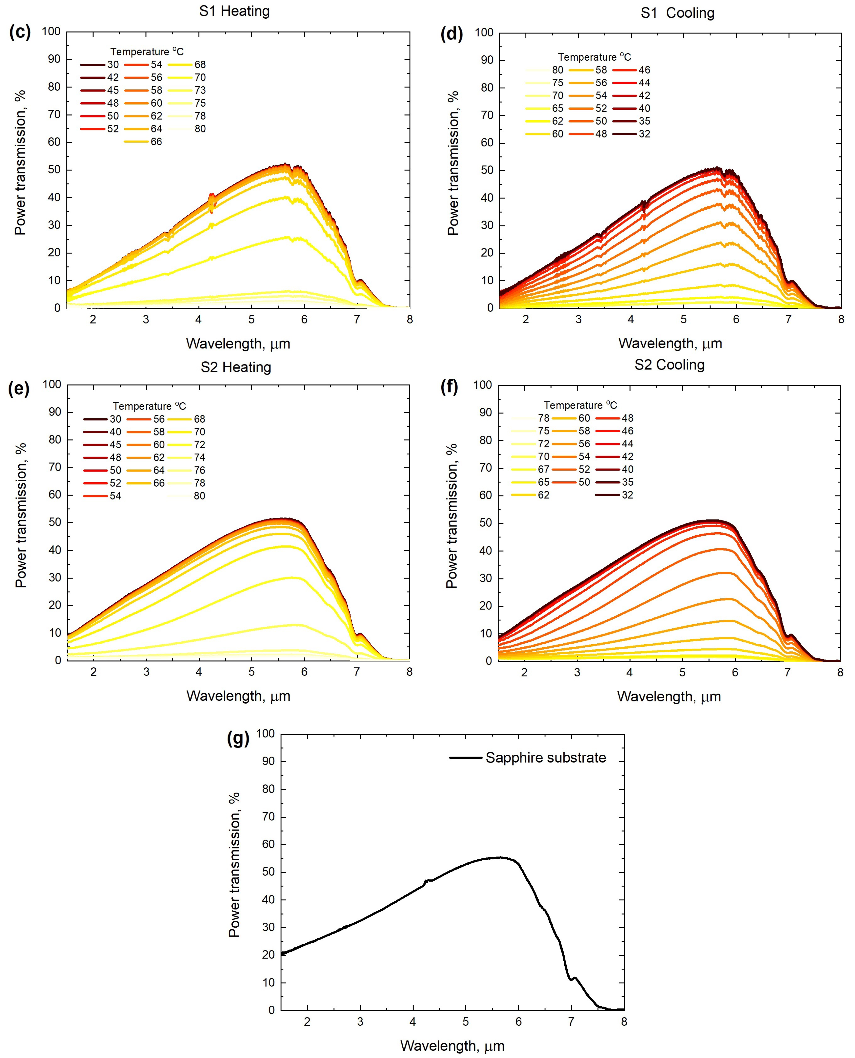
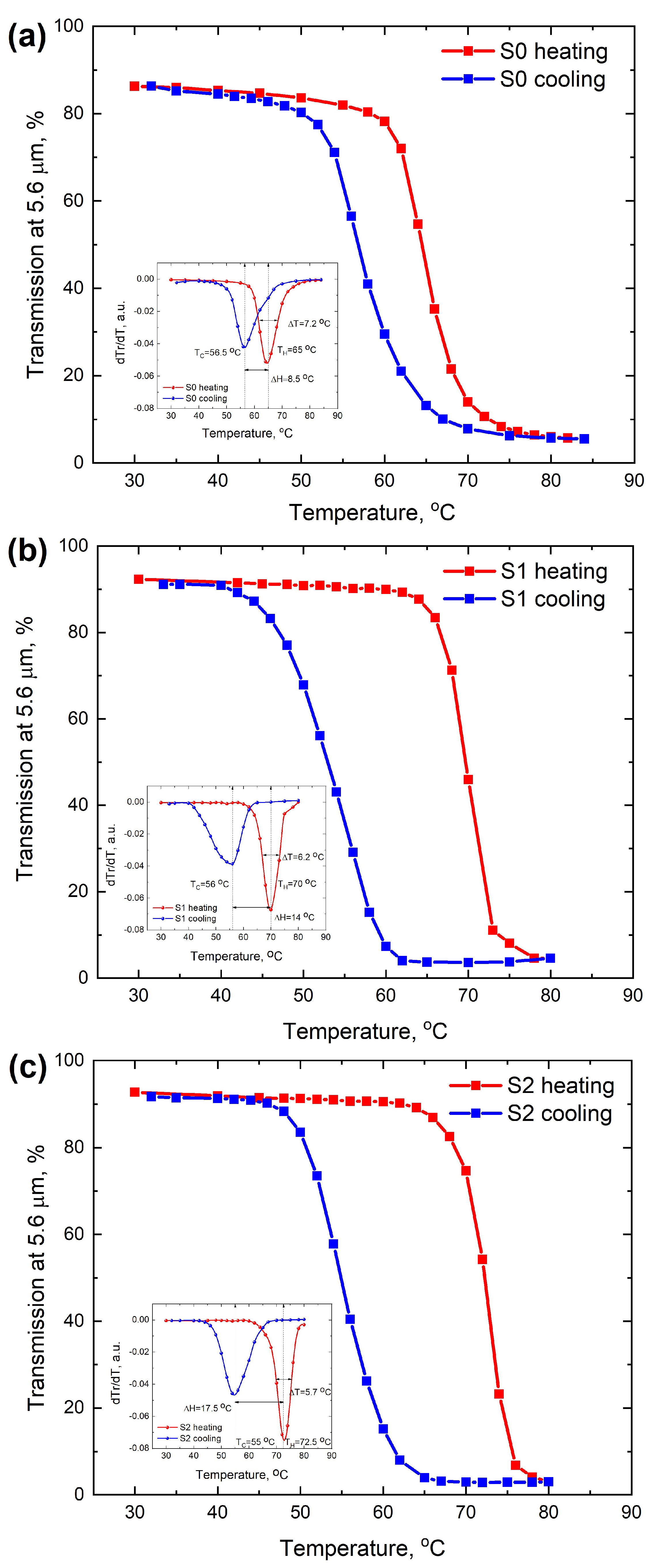
3.2. Electrical and IR Optical Properties

Figure 5 shows the resistance–temperature hysteresis loops of the undoped and Sn-doped VO 2 samples.
The resistance of the undoped sample dropped by almost 4 orders of magnitude across the phase transition. Sn-doping of VO 2 films results in an increase in the overall resistance, MIT temperature growth, and widening of thermal hysteresis loops. Moreover, with increasing Sn content, the magnitude of resistance variation tends to decrease. The incorporation of isovalent Sn 4 + ions into VO 2 does not lead to significant changes in carrier concentrations. However, doping of VO 2 generally increases the defect concentration and leads to a more distorted lattice, which as a consequence reduces the phase transition amplitude [12].
Figure 6 represents the infrared transmission of the bare sapphire substrate and VO 2 films on sapphire substrates during the heating and cooling processes. It should be noted that the optical properties of the sapphire substrate between 20 °C and 90 °C do not show a significant change as reported in [37].
The largest transmission variation takes place at 5.6 μ m, which coincides with the maximum substrate transmission. For further analysis, the hysteresis loops of IR transmission for undoped and Sn-doped VO 2 films were obtained by collecting the transmittance of films at a fixed wavelength of 5.6 μ m as shown in Figure 7. The hysteresis loops of IR transmission through VO 2 films on the sapphire substrate were normalized by transmission through the bare sapphire substrate. In order to quantitatively investigate the IR properties of VO 2 films under a phase transition, the corresponding first-order derivative curves ( d T r / d T ) of transmission variation were calculated in the insets of Figure 7.
The temperature-dependent mid-infrared properties of VO 2 films are similar to their electrical properties. To gain insight into the phase transition performance of VO 2 films with different Sn contents, several criteria were determined. The phase transition temperature was defined as the minima of the differential curves for heating ( T H ) and cooling ( T C ) processes. The hysteresis width ( Δ H ) of the phase transition was defined as the difference between phase transition temperatures during heating and cooling processes ( Δ H = T H T C ). The phase transition sharpness ( Δ T ) was characterized by the full width at half maximum (FWHM) of the d T r / d T versus the temperature curve. A smaller value of Δ T means a sharper phase transition. The modulation depth was defined as M D = ( T c o l d T h o t ) / T c o l d × 100 % , where T c o l d and T h o t are the IR transmission before and after the phase transition, respectively. The detailed parameters of the IR hysteresis loops are summarized in Table 1.
As seen from Table 1, with increasing Sn content, the width of the thermal hysteresis loop ( Δ H ) is significantly raised from 8.5 °C to 17.5 °C (sample S2). Moreover, the M D is increased from 93.7% to 96.8% and the Δ T is reduced from 7.2 °C to 5.7 °C when the Sn content increases from 0% to 1.5%. Previous reports have indicated that the grain size and grain boundary play important roles in tailoring the thermal hysteresis width [12]. Such a large hysteresis width is preferable for the development of optical-memory-type devices with a stationary memory state [38].

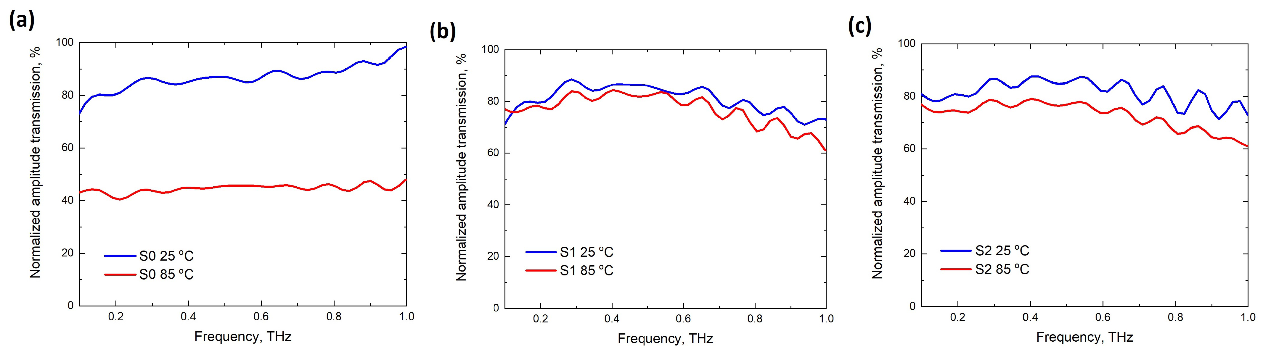
3.3. Thz Optical Properties

The optical transmission of VO 2 films with different Sn doping contents in the THz range of 0.1–1 THz was measured at 25 °C and 85 °C, respectively. The corresponding substrate-normalized THz spectra are shown in Figure 8.
The only undoped sample S0 demonstrates an obvious change in THz transmission between the two states (Figure 8a). With the addition of Sn, the amplitude modulation of THz transmission falls from an average of 49.5% to 2.9% and 10.3% for 1% and 1.5% Sn contents, respectively. An optimal Sn doping level of 1% allows for achieving the largest THz modulation damping. This is consistent with the observed reduction in conductivity after the phase transition for Sn-doped VO 2 films as seen from the electrical behavior in Figure 5. A similar relationship between electrical resistance and THz transmission has also been reported in [39,40]. This phenomenon can be attributed to the emergence of barriers between VO 2 grains upon dopant insertion. At the same time, the IR optical properties are less sensitive to the interface between the grains. Therefore, the phase transition amplitude for IR transmission varies by a small amount with Sn doping of VO 2 . The observed reduction in the temperature-driven THz amplitude modulation in conjunction with high IR transmission modulation for Sn-doped VO 2 films can be considered as a basis for the development of dichroic optical elements. This feature can be utilized for the separation of generated THz radiation from the initial mid-infrared spectral part in intense THz pulse generation using two-color filamentation techniques [41,42].

4. Conclusions

In summary, a series of VO 2 films with different Sn doping contents were prepared on a sapphire substrate by hydrothermal synthesis and a post-annealing process. It was revealed that using (NH 4 ) 2 SnF 6 as a Sn precursor allows producing homogeneous Sn-doped VO 2 films. For IR transmission, the hysteresis width of VO 2 films can be increased to 17.5 °C by Sn doping. For THz transmission, a suppression of the temperature-driven modulation after Sn doping is observed. This work provides a new mode for the development of dichroic optical components, e.g., a temperature-switchable infrared element with transparency in the THz range.

Author Contributions

Conceptualization, M.K.; methodology, O.B.; resources, G.K.; measurement, A.G., A.S. and I.R.; sample fabrication, A.T. and O.M.; writing—original draft preparation, A.G.; writing—review and editing, A.G., O.B. and M.K.; supervision, M.K.; funding acquisition, G.K. All authors have read and agreed to the published version of the manuscript.

Funding

This research received no external funding. This work was performed using the resources of Tydex LLC.

Data Availability Statement

The data that support the findings of this study are available from the corresponding author upon reasonable request.

Acknowledgments

Experimental studies were carried out on the equipment of the core shared research facilities “Composition, structure and properties of structural and functional materials” of the NRC “Kurchatov Institute”—CRISM “Prometey”. SEM was performed using the equipment of the JRC PMR IGIC RAS. The synthesis of films was realized with assistance LLC UGO.

Conflicts of Interest

The authors declare that they have no known competing financial interests or personal relationships that could have appeared to influence the work reported in this paper.

Abbreviations

The following abbreviations are used in this manuscript:
SnTin
VO 2 Vanadium dioxide
IRInfrared
THzTerahertz
XRDX-ray diffraction
SEMScanning electron microscopy
MITMetal–insulator transition
EGEthylene glycol
DIDeionized
THz-TDSTerahertz time-domain spectroscopy
FWHMFull width at half maximum

References

  1. Tittl, A.; Michel, A.K.U.; Schäferling, M.; Yin, X.; Gholipour, B.; Cui, L.; Wuttig, M.; Taubner, T.; Neubrech, F.; Giessen, H. A switchable mid-infrared plasmonic perfect absorber with multispectral thermal imaging capability. Adv. Mater. 2015, 27, 4597–4603. [Google Scholar] [CrossRef]
  2. Pang, X.; Ozolins, O.; Jia, S.; Zhang, L.; Schatz, R.; Udalcovs, A.; Bobrovs, V.; Hu, H.; Morioka, T.; Sun, Y.T.; et al. Bridging the Terahertz Gap: Photonics-assisted Free-Space Communications from the Submillimeter-Wave to the Mid-Infrared. J. Light. Technol. 2022, 40, 3149–3162. [Google Scholar] [CrossRef]
  3. Lin, H.; Luo, Z.; Gu, T.; Kimerling, L.C.; Wada, K.; Agarwal, A.; Hu, J. Mid-infrared integrated photonics on silicon: A perspective. Nanophotonics 2018, 7, 393–420. [Google Scholar] [CrossRef]
  4. Fang, Y.; Ge, Y.; Wang, C.; Zhang, H. Mid-infrared photonics using 2D materials: Status and challenges. Laser Photonics Rev. 2020, 14, 1900098. [Google Scholar] [CrossRef]
  5. Shu, F.Z.; Wang, J.N.; Peng, R.W.; Xiong, B.; Fan, R.H.; Gao, Y.J.; Liu, Y.; Qi, D.X.; Wang, M. Electrically Driven Tunable Broadband Polarization States via Active Metasurfaces Based on Joule-Heat-Induced Phase Transition of Vanadium Dioxide. Laser Photonics Rev. 2021, 15, 2100155. [Google Scholar] [CrossRef]
  6. Erçağlar, V.; Hajian, H.; Özbay, E. VO2–graphene-integrated hBN-based metasurface for bi-tunable phonon-induced transparency and nearly perfect resonant absorption. J. Phys. Appl. Phys. 2021, 54, 245101. [Google Scholar] [CrossRef]
  7. Liu, L.; Kang, L.; Mayer, T.S.; Werner, D.H. Hybrid metamaterials for electrically triggered multifunctional control. Nat. Commun. 2016, 7, 13236. [Google Scholar] [CrossRef] [PubMed]
  8. Dicken, M.J.; Aydin, K.; Pryce, I.M.; Sweatlock, L.A.; Boyd, E.M.; Walavalkar, S.; Ma, J.; Atwater, H.A. Frequency tunable near-infrared metamaterials based on VO2 phase transition. Opt. Express 2009, 17, 18330–18339. [Google Scholar] [CrossRef] [PubMed] [Green Version]
  9. Kats, M.A.; Blanchard, R.; Genevet, P.; Yang, Z.; Qazilbash, M.M.; Basov, D.; Ramanathan, S.; Capasso, F. Thermal tuning of mid-infrared plasmonic antenna arrays using a phase change material. Opt. Lett. 2013, 38, 368–370. [Google Scholar] [CrossRef]
  10. Liu, Z.M.; Li, Y.; Zhang, J.; Huang, Y.Q.; Li, Z.P.; Pei, J.H.; Fang, B.Y.; Wang, X.H.; Xiao, H. Design and fabrication of a tunable infrared metamaterial absorber based on VO2 films. J. Phys. Appl. Phys. 2017, 50, 385104. [Google Scholar] [CrossRef]
  11. Kats, M.A.; Sharma, D.; Lin, J.; Genevet, P.; Blanchard, R.; Yang, Z.; Qazilbash, M.M.; Basov, D.; Ramanathan, S.; Capasso, F. Ultra-thin perfect absorber employing a tunable phase change material. Appl. Phys. Lett. 2012, 101, 221101. [Google Scholar] [CrossRef] [Green Version]
  12. Xue, Y.; Yin, S. Element doping: A marvelous strategy for pioneering the smart applications of VO2. Nanoscale 2022, 14, 11054–11097. [Google Scholar] [CrossRef] [PubMed]
  13. Ke, Y.; Wang, S.; Liu, G.; Li, M.; White, T.J.; Long, Y. Vanadium dioxide: The multistimuli responsive material and its applications. Small 2018, 14, 1802025. [Google Scholar] [CrossRef] [PubMed]
  14. Morin, F. Oxides which show a metal-to-insulator transition at the Neel temperature. Phys. Rev. Lett. 1959, 3, 34. [Google Scholar] [CrossRef]
  15. Liu, K.; Lee, S.; Yang, S.; Delaire, O.; Wu, J. Recent progresses on physics and applications of vanadium dioxide. Mater. Today 2018, 21, 875–896. [Google Scholar] [CrossRef] [Green Version]
  16. Shi, R.; Shen, N.; Wang, J.; Wang, W.; Amini, A.; Wang, N.; Cheng, C. Recent advances in fabrication strategies, phase transition modulation, and advanced applications of vanadium dioxide. Appl. Phys. Rev. 2019, 6, 011312. [Google Scholar] [CrossRef]
  17. Ji, H.; Liu, D.; Cheng, H. Infrared optical modulation characteristics of W-doped VO2 (M) nanoparticles in the MWIR and LWIR regions. Mater. Sci. Semicond. Process. 2020, 119, 105141. [Google Scholar] [CrossRef]
  18. Lv, X.; Chai, X.; Lv, L.; Cao, Y.; Zhang, Y.; Song, L. Preparation of porous Mo-doped VO2 films via atomic layer deposition and post annealing. Jpn. J. Appl. Phys. 2021, 60, 085501. [Google Scholar] [CrossRef]
  19. Guan, S.; Souquet-Basiège, M.; Toulemonde, O.; Denux, D.; Penin, N.; Gaudon, M.; Rougier, A. Toward room-temperature thermochromism of VO2 by Nb doping: Magnetic investigations. Chem. Mater. 2019, 31, 9819–9830. [Google Scholar] [CrossRef]
  20. Victor, J.L.; Gaudon, M.; Salvatori, G.; Toulemonde, O.; Penin, N.; Rougier, A. Doubling of the phase transition temperature of VO2 by Fe doping. J. Phys. Chem. Lett. 2021, 12, 7792–7796. [Google Scholar] [CrossRef]
  21. Chen, S.; Liu, J.; Wang, L.; Luo, H.; Gao, Y. Unraveling mechanism on reducing thermal hysteresis width of VO2 by Ti doping: A joint experimental and theoretical study. J. Phys. Chem. C 2014, 118, 18938–18944. [Google Scholar] [CrossRef]
  22. Nishikawa, M.; Nakajima, T.; Kumagai, T.; Okutani, T.; Tsuchiya, T. Adjustment of thermal hysteresis in epitaxial VO2 films by doping metal ions. J. Ceram. Soc. Jpn. 2011, 119, 577–580. [Google Scholar] [CrossRef] [Green Version]
  23. Yano, A.; Clarke, H.; Sellers, D.G.; Braham, E.J.; Alivio, T.E.; Banerjee, S.; Shamberger, P.J. Toward high-precision control of transformation characteristics in VO2 through dopant modulation of hysteresis. J. Phys. Chem. C 2020, 124, 21223–21231. [Google Scholar] [CrossRef]
  24. Gao, Z.; Liu, Z.; Ping, Y.; Ma, Z.; Li, X.; Wei, C.; He, C.; Liu, Y. Low metal–insulator transition temperature of Ni-doped vanadium oxide films. Ceram. Int. 2021, 47, 28790–28796. [Google Scholar] [CrossRef]
  25. Zou, Z.; Zhang, Z.; Xu, J.; Yu, Z.; Cheng, M.; Xiong, R.; Lu, Z.; Liu, Y.; Shi, J. Thermochromic, threshold switching, and optical properties of Cr-doped VO2 thin films. J. Alloys Compd. 2019, 806, 310–315. [Google Scholar] [CrossRef]
  26. Schläefer, J.; Sol, C.; Li, T.; Malarde, D.; Portnoi, M.; Macdonald, T.J.; Laney, S.K.; Powell, M.J.; Top, I.; Parkin, I.P.; et al. Thermochromic VO2-SiO2 nanocomposite smart window coatings with narrow phase transition hysteresis and transition gradient width. Sol. Energy Mater. Sol. Cells 2019, 200, 109944. [Google Scholar] [CrossRef]
  27. Zhao, Z.; Liu, Y.; Wang, D.; Ling, C.; Chang, Q.; Li, J.; Zhao, Y.; Jin, H. Sn dopants improve the visible transmittance of VO2 films achieving excellent thermochromic performance for smart window. Sol. Energy Mater. Sol. Cells 2020, 209, 110443. [Google Scholar] [CrossRef]
  28. Zhao, Z.; Liu, Y.; Yu, Z.; Ling, C.; Li, J.; Zhao, Y.; Jin, H. Sn–W Co-doping improves thermochromic performance of VO2 films for smart windows. ACS Appl. Energy Mater. 2020, 3, 9972–9979. [Google Scholar] [CrossRef]
  29. Naftaly, M. Terahertz Metrology; Artech House: Boston, MA, USA, 2015. [Google Scholar]
  30. THz Spectral Splitters. Available online: https://www.tydexoptics.com/products/thz_optics/thz_splitter (accessed on 5 June 2023).
  31. Bauer, T.; Kolb, J.; Löffler, T.; Mohler, E.; Roskos, H.; Pernisz, U. Indium–tin–oxide-coated glass as dichroic mirror for far-infrared electromagnetic radiation. J. Appl. Phys. 2002, 92, 2210–2212. [Google Scholar] [CrossRef]
  32. Lai, W.; Yuan, H.; Fang, H.; Zhu, Y.; Wu, H. Ultrathin, highly flexible and optically transparent terahertz polarizer based on transparent conducting oxide. J. Phys. D Appl. Phys. 2020, 53, 125109. [Google Scholar] [CrossRef]
  33. Chen, C.W.; Lin, Y.C.; Chang, C.H.; Yu, P.; Shieh, J.M.; Pan, C.L. Frequency-dependent complex conductivities and dielectric responses of indium tin oxide thin films from the visible to the far-infrared. IEEE J. Quantum Electron. 2010, 46, 1746–1754. [Google Scholar] [CrossRef]
  34. Arezoomandan, S.; Prakash, A.; Chanana, A.; Yue, J.; Mao, J.; Blair, S.; Nahata, A.; Jalan, B.; Sensale-Rodriguez, B. THz characterization and demonstration of visible-transparent/terahertz-functional electromagnetic structures in ultra-conductive La-doped BaSnO3 Films. Sci. Rep. 2018, 8, 3577. [Google Scholar] [CrossRef] [Green Version]
  35. Ivanov, A.V.; Tatarenko, A.Y.; Gorodetsky, A.A.; Makarevich, O.N.; Navarro-Cia, M.; Makarevich, A.M.; Kaul, A.R.; Eliseev, A.A.; Boytsova, O.V. Fabrication of epitaxial W-doped VO2 nanostructured films for terahertz modulation using the solvothermal process. ACS Appl. Nano Mater. 2021, 4, 10592–10600. [Google Scholar] [CrossRef]
  36. Shvets, P.; Dikaya, O.; Maksimova, K.; Goikhman, A. A review of Raman spectroscopy of vanadium oxides. J. Raman Spectrosc. 2019, 50, 1226–1244. [Google Scholar] [CrossRef]
  37. Thomas, M.E.; Joseph, R.I.; Tropf, W.J. Infrared transmission properties of sapphire, spinel, yttria, and ALON as a function of temperature and frequency. Appl. Opt. 1988, 27, 239–245. [Google Scholar] [CrossRef] [PubMed]
  38. Lu, C.; Lu, Q.; Gao, M.; Lin, Y. Dynamic manipulation of THz waves enabled by phase-transition VO2 thin film. Nanomaterials 2021, 11, 114. [Google Scholar] [CrossRef] [PubMed]
  39. Wu, X.; Wu, Z.; Ji, C.; Zhang, H.; Su, Y.; Huang, Z.; Gou, J.; Wei, X.; Wang, J.; Jiang, Y. THz transmittance and electrical properties tuning across IMT in vanadium dioxide films by Al doping. ACS Appl. Mater. Interfaces 2016, 8, 11842–11850. [Google Scholar] [CrossRef]
  40. Ji, C.; Wu, Z.; Wu, X.; Feng, H.; Wang, J.; Huang, Z.; Zhou, H.; Yao, W.; Gou, J.; Jiang, Y. Optimization of metal-to-insulator phase transition properties in polycrystalline VO2 films for terahertz modulation applications by doping. J. Mater. Chem. C 2018, 6, 1722–1730. [Google Scholar] [CrossRef]
  41. Fedorov, V.Y.; Tzortzakis, S. Optimal wavelength for two-color filamentation-induced terahertz sources. Opt. Express 2018, 26, 31150–31159. [Google Scholar] [CrossRef]
  42. Koulouklidis, A.D.; Gollner, C.; Shumakova, V.; Fedorov, V.Y.; Pugžlys, A.; Baltuška, A.; Tzortzakis, S. Observation of extremely efficient terahertz generation from mid-infrared two-color laser filaments. Nat. Commun. 2020, 11, 292. [Google Scholar] [CrossRef] [Green Version]
Figure 1. SEM morphology view of the VO 2 films: (a) S0, (b) S1, and (c) S2.
Ceramics 06 00079 g001
Figure 2. SEM cross-sectional view of the VO 2 films: (a) S0, (b) S1, and (c) S2.
Ceramics 06 00079 g002
Figure 3. XRD spectra of undoped and Sn-doped VO 2 films. The marker “*” indicates the reflection from the stainless sample table.
Ceramics 06 00079 g003
Figure 4. Raman spectra of the sapphire substrate and undoped and Sn-doped VO 2 films.
Ceramics 06 00079 g004
Figure 5. Electrical resistance of the VO 2 films as a function of temperature during heating and cooling cycles.
Ceramics 06 00079 g005
Figure 6. Infrared transmission spectra of the undoped VO 2 film (a,b), Sn-doped VO 2 films (cf) on sapphire substrates during heating and cooling cycles, and the bare sapphire substrate (g).
Ceramics 06 00079 g006aCeramics 06 00079 g006b
Figure 7. Normalized maximum power transmission at 5.6 μ m through undoped (a) and Sn-doped (b,c) VO 2 films on a sapphire substrate during heating and cooling cycles.
Ceramics 06 00079 g007
Figure 8. Normalized terahertz transmission spectra through undoped (a) and Sn-doped VO 2 films on a sapphire substrate (b,c).
Ceramics 06 00079 g008
Table 1. Parameters of hysteresis loops at 5.6 μ m for VO 2 films.
SampleMD, % Δ H , °C Δ T , °C
S093.78.57.2
S195146.2
S296.817.55.7
Disclaimer/Publisher’s Note: The statements, opinions and data contained in all publications are solely those of the individual author(s) and contributor(s) and not of MDPI and/or the editor(s). MDPI and/or the editor(s) disclaim responsibility for any injury to people or property resulting from any ideas, methods, instructions or products referred to in the content.

