Article

Fabrication of Segments for ZnO-Based Tube Ceramic Targets by the Spark Plasma Sintering Method

by
Akhmed K. Akhmedov
1,
Abil Sh. Asvarov
2,*,
Soslan Sh. Makhmudov
1 and
Vladimir M. Kanevsky
2
1
Institute of Physics, Dagestan Research Center of Russian Academy Sciences, Yaragskogo Str., 94, 367015 Makhachkala, Russia
2
Shubnikov Institute of Crystallography, Federal Scientific Research Center “Crystallography and Photonics” of Russian Academy of Sciences, Leninsky Prospect, 59, 119333 Moscow, Russia
*
Author to whom correspondence should be addressed.
Ceramics 2023, 6(3), 1302-1313; https://doi.org/10.3390/ceramics6030080
Submission received: 31 May 2023 / Revised: 14 June 2023 / Accepted: 20 June 2023 / Published: 21 June 2023

Abstract

:
In this article, problems associated with the fabrication of ZnO-based ceramics in the form of large-diameter hollow cylinders with a large ratio of height h to wall thickness ∆r (h/∆r ≥ 3) by the spark plasma sintering (SPS) method were studied. The design of the press-form is proposed, which ensures the reduction in temperature gradients along the inner and outer surfaces of the hollow cylindrical sintered body and, as a result, the achievement of a high-density uniformity of the sintered body over its volume. A hollow cylindrical ZnO-based ceramic sample considered as segments of TCO tube targets with outer diameter D = 72 mm, inner diameter d = 47 mm, and height h = 36 mm were fabricated. The sample had a relative density of more than 98.5% of the theoretical density for a given composition with a minimal density inhomogeneity along the height of the sample. The microstructure of the obtained ceramics was studied using the SEM and XRD methods.
Keywords:
SPS; ZnO; ceramic; tube target; TCO

Graphical Abstract

1. Introduction

The industrial implementation of magnetron sputtering for various large-scale coating applications has been accompanied by various milestones. One of important milestones, dated to the 1990s, is the practice to replace planar targets with cylindrical targets in rotatable cathodes since, in planar sputter targets, target utilization for normal cathodes can reach 40% (by using special designs of moveable magnet configurations), whereas for a cylindrical target, the target utilization is generally in a range between 75 and 90% [1,2,3].
Besides the utilization, rotatables have fewer tendencies for arcing and can also run at higher power densities than planar targets due to the maximum heating zone is evenly distributed over the whole tube target surface. Accordingly, cylindrical targets maximize greatly both intervals between scheduled maintenance of industrial sputtering equipment and their up-time [2]. In light of these advantages, currently, the deposition of transparent conducting oxide (TCO) thin films by rotatable magnetron sputtering is a generally accepted industrial standard [3,4].
The main drawback of rotatable magnetrons with tube targets is that the target production is more complex and more expensive, especially in the case of ceramic target materials [3]. It is obvious that metallic tube targets are easier to produce than the comparatively brittle ceramic targets. Many metals can be made into a single piece or monolithic targets that are machined from thick tubing or billet. For pure metal and alloy tube targets, a two-layer structure can be also formed using manufacturing techniques that either spray the metal or press a metallic powder into a solid on the surface of a titanium or stainless-steel backing tube [5].
In the case of ceramic sputtering materials, a three-layer design of a tubular target is usually used, in which the material of the ceramic target in the form of multiple hollow cylinder segments is strung and bonded on the stainless-steel backing tube. Indium is usually used as a bonding material between the ceramic segments and the backing tube. The segmentation of the ceramic material and its bonding by indium reduce stresses that could cause the target material to break [4,5].
At present, the main technique for obtaining TCO ceramic targets is the pressing-free sintering of a green body preformed in various ways (slip casting, uniaxial, and cold isostatic press methods) [6,7,8,9]. This technique is characterized by significant shrinkage during sintering, and as a result, a high probability of deformation of the sintered material expected. When sintering ceramics with a complex shape (hollow, elongated, thin-walled, etc.), these negative phenomena significantly reduce the yield of good products and increase material consumption due to the need for high allowances for finishing post-machining.
At the same time, other types of sintering methods, such as hot isostatic pressing (HIP), uniaxial hot pressing (UHP), and spark plasma sintering (SPS), which provide simultaneous high-temperature and pressing effects on the sintered material, look like very promising techniques for forming cylindrical segments of tube targets. Gao M et al. showed that HIP was a suitable technology to fabricate the Al-doped ZnO targets with ultra-high density and improved homogeneity [10]. They had declaimed a successful preparation of industrial-size ZnO-based rectangular targets with over 100% density (5.66 g/cm3). In turn, Lee J.-R. et al. showed that the use of a UHP procedure at the stage of forming cylindrical segments for ZnO-based tube targets can significantly reduce a tapering phenomenon along the formed cylinder characteristic of pressure-free sintering. [11]. It is also important to note that the use of rigid and rugged press-forms in the one stage UHP and SPS techniques also ensures the formation of a sintered ceramic body with dimensions very close to the required final dimensions, which minimizes subsequent machining processes. Moreover, UHP and SPS equipment is less expensive and less bulky than it is for the case of the HIP process [12].
The SPS method is essentially a modification of UHP, since during SPS sintering, electrical current is passed directly through the press-form and the formed material and not through an external heater [13]. SPS synthesis is characterized by a short duration of the high-temperature phase of the technological cycle and a significant decrease in the integral temperature of synthesis, which prevents the growth of grains [14]. The short duration of the high-temperature phase of the sintering process also contributes to the preservation of the initial stoichiometric composition, which is especially important when sintering components with widely differing thermal properties [15]. In addition, the passing of powerful current pulses through the formed material contributes to the activation of solid-phase diffusion processes and gas-phase microplasma physicochemical reactions in interparticle contact areas, which results in earlier compaction of a sintered ceramic body and preservation of its fine-grained structure.
There are several reports about a successful preparation of dense oxide ceramics by the SPS technique for TCO, thermoelectric, and scintillation applications [16,17,18,19,20,21]. Unfortunately, mostly they dealt with disk-shape samples of small sizes. However, it is obvious that the aspects of scalability and complication of the shape of the final product, which emerge in the live issue of the SPS production of targets for the TCO industry, will require the optimization not only of the technological modes of sintering of a particular material but also of the tooling components of the SPS setup [22].
In the present work, we study the problems associated with the production of hollow cylindrical products by spark plasma sintering, in which the ratio of the cylinder height h to the wall thickness ∆r is greater than or equal to 3. Some technological solutions have been proposed that provide a reduction in temperature gradients along the outer and inner surfaces of the sintered material. ZnO-based TCO material, namely ZnO co-doped with Ga (3 at.%) and B (0.2 at.%), was taken as the object of study [23].

2. Materials and Methods

Submicron-sized zinc oxide (99.95% purity) and micron-sized boric acid (99.9% purity) in the form of powders, as well as metallic gallium (99.999% purity), were used as starting materials in the preparation of Ga, B-codoped ZnO (GZOB) ceramics. The powder mixture preparation procedure for the SPS synthesis of the ceramics was similar to that described in detail earlier [24]. The uniformity of filling the powder mixture into the inside of a press-form (PF) was ensured by preliminary granulation, which consists of gently forcing the moistened mixture through a 250 US mesh sieve. The granulation resulted in a more than twofold increase in the backfill density of the mixture to a value of 2.1 g/cm3 due to the formation at this stage of many round-shaped granules with sizes from 5 to 50 μm (Figure S1 of the Supplementary Materials).
For sintering ceramic samples, a homemade laboratory SPS unit was used [15]. Sintering was carried out under a fore-vacuum condition at a base pressure P less than 1 Pa using PFs made of isostatic graphite-grade ISEM-3. Two types of PFs have been used to sinter ceramics. To optimize the sintering temperatures, a PF was used to form flat-disk samples with a diameter of 38 mm and a thickness of 4 mm, while a more complex PF was used to obtain cylindrical hollow samples (Figure S2 of Supplementary Materials), the details of which will be given in the next section. To exclude the interaction of the PF elements with the sintered oxide material, all surfaces of the PFs in contact with the oxide mixture were protected by graphite foil inserts.
The applied pressure for all samples during SPS sintering, based on the mechanical strength of the graphite PFs used, was set at 30 MPa. The temperature rise to operating values was carried out at a rate of 50 °C/min due to the relatively low thermal conductivity of the oxide mixture at the initial stage of sintering and the need to ensure complete degassing of the compacted mixture before the start of the main sintering. The sintering time for all samples at a given sintering temperature TSPS was 5 min.
After removing a sintered sample from the cooled PF, it was freed from the outer baked shell of graphite foil by SiC sand polish for its subsequent characterization. To study the homogeneity, cylindrical hollow samples were also subjected to diamond cutting.
The physical densities of the sintered ceramic samples were measured by the Archimedes method (balances OHAUS Adventurer™ Analytical AX 124 (OHAUS®, Parsippany, NJ, USA), according to Equation (1):
ϱ s = ϱ w × m a / ( m a m w ) ,
where ϱ s is the density of the sample, ϱ w = 0.997 g/cm3 is the density of the water at 27 °C, m a is the weight of the specimen in air, and m w is the weight of the specimen in water.
For the theoretical density of the bulk Ga, B-codoped ZnO, according to a rule of mixtures between the volume fractions of components [25], the value of ϱ t = 5.67 g/cm3 was taken for the mix system of 98.7 mol% ZnO + 1.5 mol% Ga2O3 + 0.1 mol% B2O3. Further, the relative density ϱ % of the sintered samples was determined in accordance with Equation (2):
ϱ % = 100 % × ( ϱ s / ρ t ) ,
The structure of the ceramic samples was determined by X-ray diffraction (XRD, PANalytical X’PERT PRO MPD diffractometer, Malvern Panalytical B.V., Almelo, Netherlands) with a Cu-Kα radiation source in the 2θ range of 30–70°. The morphology of fracture surfaces of the sintered ceramic samples was carried out by the scanning electron microscopy (SEM, Leo-1450 microscope).

3. Results

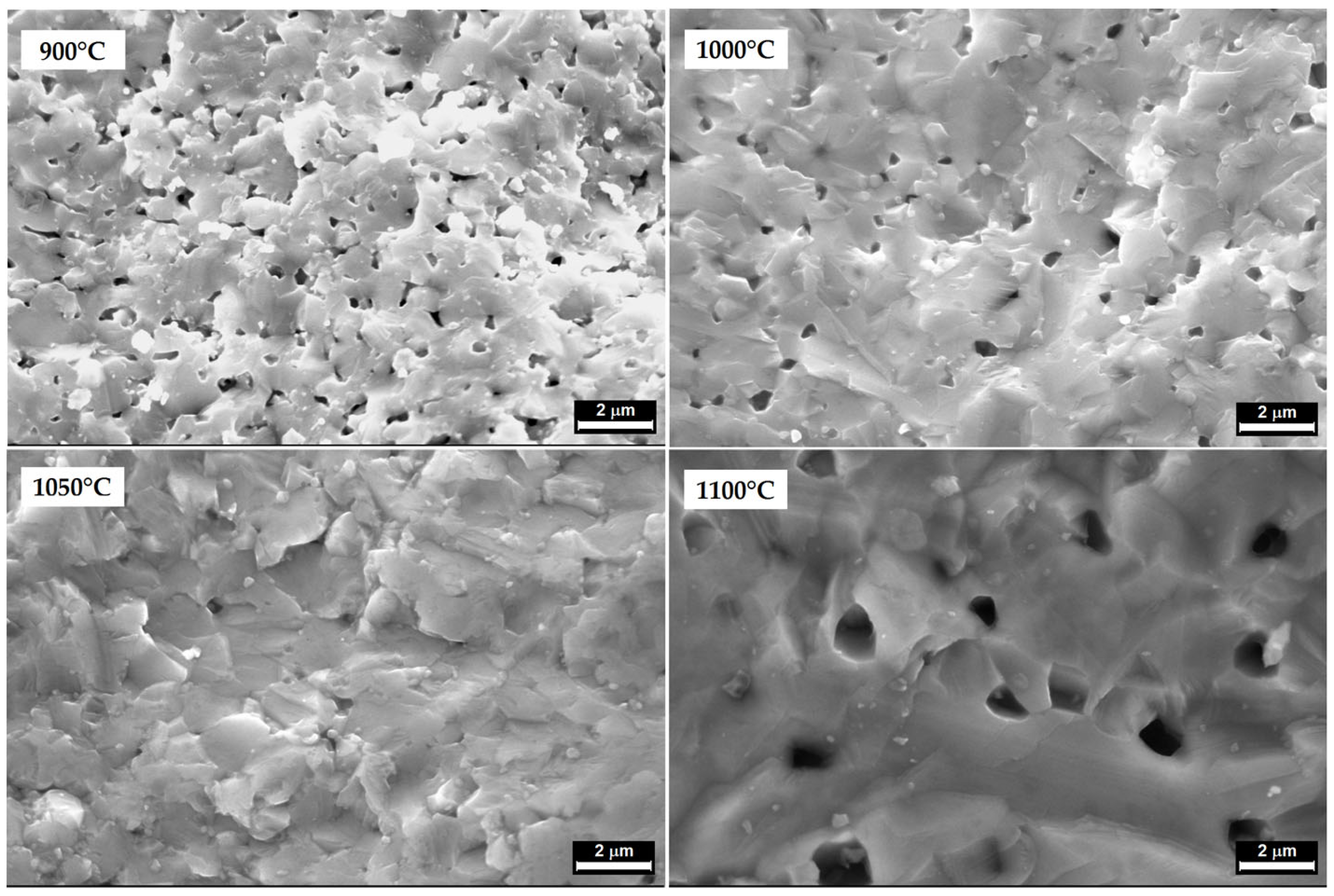
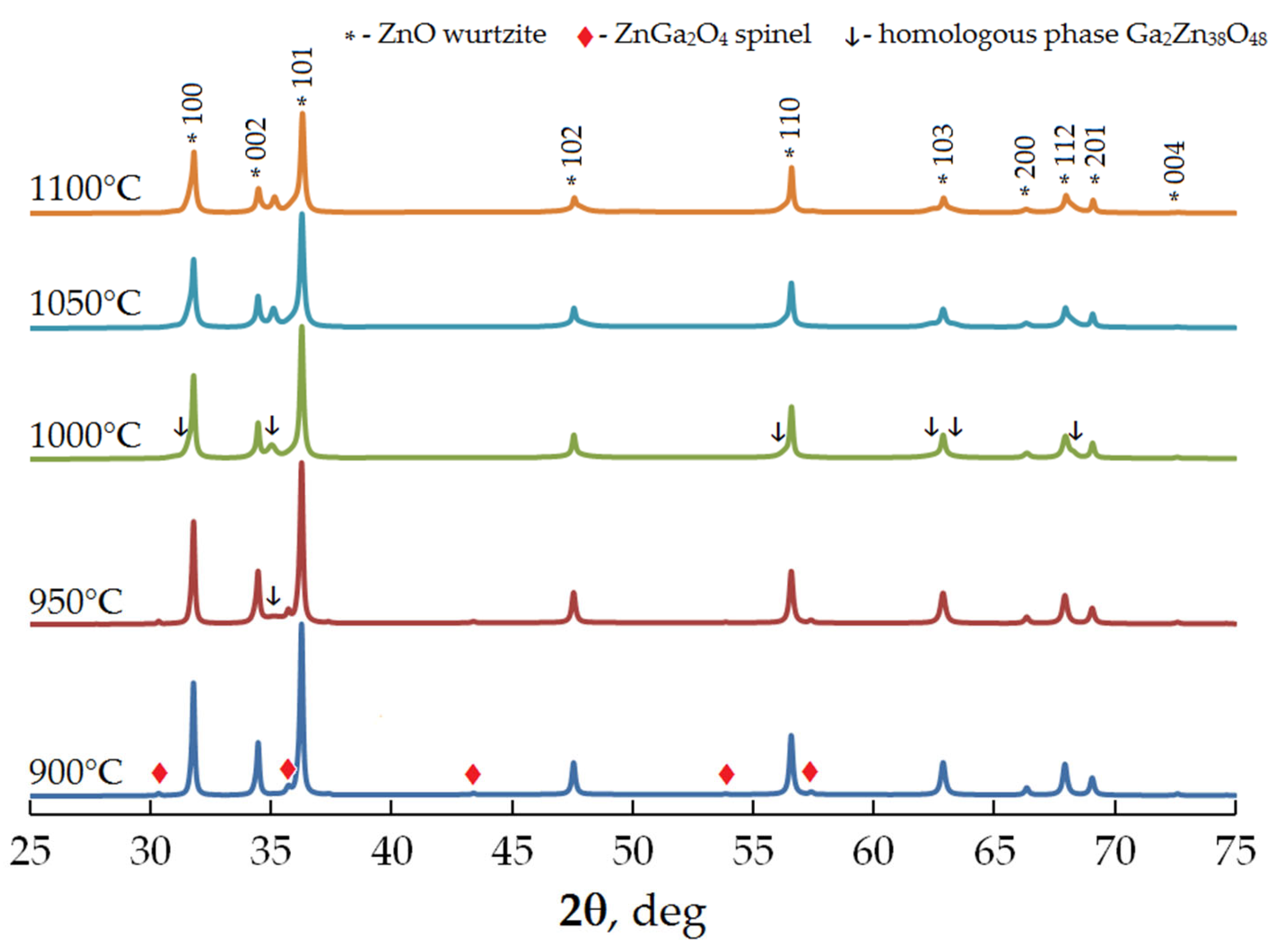
3.1. Optimization of the Temperature Regime of Spark Plasma Sintering of GZOB

First, optimization of the sintering temperature TSPS of the GZOB material in order to achieve a density ϱ % > 98% acceptable for practical use was carried out during SPS formation of disk samples with a diameter of 38 mm and a thickness of 5 mm. Figure 1 shows a photograph of GZOB disk samples sintered at different TSPS.
It can be seen that the color of the GZOB samples changes at different sintering temperatures: from gray-yellow (900 °C) to green (1000 °C) and dark green (1100 °C). The change in color in the GZOB ceramics is caused by a high level of doping with Ga [26], an introduction of different defects in ZnO (VO and Zni) [27] and a shift from lower density to higher density [28,29].
The values of physical density ϱ s and relative density ϱ % of the GZOB ceramics sintered at different TSPS are shown in Figure 2. The relative density of the samples increases with temperature until 1050 °C is reached and then decreases. The highest density (99.2%) was obtained at 1050 °C, which is lower than the temperature for the case of the traditional sintering of pre-molded ZnO-based compacts by a solid-state reaction method. As reported in ZnO, for ceramics sintered by a solid-state reaction method [16,24,30,31], at least 1200 °C is required to attain high density for ceramic ZnO materials with same doping levels.
Figure 3 shows the fracture morphology of the GZOB samples sintered at different TSPS for the superfast densification process by SPS. The SEM micrographs obviously show that the grain size increases with TSPS. A gradual transition from the isotropic shape of the particles to the anisotropic one is also observed with increasing TSPS. When the temperature increases up to 1050 °C, some grain growth through an integration phenomenon between grains and pore exclusion become serious. However, at TSPS above 1050 °C, the grain size quickly increases, and large pores appear at the boundaries of coarse grains.
It is obvious that some part of the metal oxide tends to decompose under special effects of the large electric current and a high-temperature vacuum environment in the SPS process. At a higher sintering temperature, the decomposition of zinc oxide is expected to be very serious [10,27]. Since the SPS compaction process is superfast, the gaseous decomposition products intensively formed into the ZnO ceramic at 1100 °C contribute to the formation of closed porosity, thereby reducing the final density of sintered ceramics.
The XRD patterns of GZOB ceramics are shown in Figure 4. All XRD patterns correspond to the hexagonal ZnO (JCPDF #75-0576) phase as the main component. ZnGa2O4 impurity peaks were identified for the sample synthesized at T = 900 °C. However, the secondary spinel phase peak intensities were several orders of magnitude lower than that of the main phase.
It has been reported that in the case of high doping concentration (above the impurity solubility limit), a lot of secondary spinel phase products would form in doped ZnO ceramics under high-temperature treatments [32,33]. The spinel peaks were also present in the XRD pattern of the sample sintered at TSPS = 950 °C. However, in the spectrum of this sample, a shoulder above the background level was observed to the right of the 002 ZnO peak (it is marked with an arrow in the spectrum second from the bottom). This phenomenon may be due to the nucleation of an additional secondary phase.
With a further increase in TSPS, the signs of this additional phase become more distinct, while the spinel phase ZnGa2O4 disappears completely. On the XRD patterns of GZOB samples sintered at TSPS above 950 °C, a diffraction peak appears at 2θ ≅ 35.1°, and there is a clear asymmetry of some peaks of the ZnO wurtzite phase. As the temperature rises, this phenomenon intensifies.
The secondary phase in the Ga-doped ZnO samples had been identified as Ga2Zn9O12 in some reports [32,34,35]. However, no significant peak from Ga2Zn9O12 should appear at this position in the XRD patterns. Ga2Zn9O12 is a member of the homologous series Ga2ZnmOm+3 (m: natural number). Michiue et al. have demonstrated that in the Ga–Zn–O system with a large Zn/Ga ratio, the appearance of a peak at 2θ ≅ 35.1° is well described by the formation of a two-phase system consisting of Ga-doped ZnO (wurtzite structure) as a dominant component and the homologous phase Ga2ZnmOm+3, where m is close to 38 [36]. It is also noted by them that the diffraction pattern of the homologous phase Ga2ZnmOm+3 shows an increasing resemblance to that of the wurtzite structure with increasing m because the structures of Ga2ZnmOm+3 are closely related to the wurtzite structure [37].
Thus, the XRD studies show that the following phase transformation is observed in our GZOB material with increasing TSPS:
Z n O + G a 2 O 3 up to   950   ° C   &   B Z n O : G a + Z n G a 2 O 4 a b o v e   950   ° C   &   B Z n O : G a + G a 2 Z n 38 O 41 ,
where a small addition of B in the oxide form is a sintering aid through creating conditions for the phase transformations to proceed in a quasi-closed volume [32,38].
Both final phase transformation products, the ZnO:Ga wurtzite phase and the homologous compound Ga2ZnmOm+3, are inherently a sign of an ultra-uniform distribution of the Ga dopant ions over the ZnO host volume. It is also worth noting here that SPS made it possible to achieve an efficient distribution of Ga dopant into the ZnO host at lower temperatures than in the case of the traditional solid-state reaction method.
Accordingly, our SPS experiments with disk-shaped GSZOB ceramic samples have shown that the optimal SPS temperature in order to obtain high-density homogeneous TCO targets is 1050 °C.

3.2. Optimization of the SPS Process for Hollow Cylindrical GZOB Ceramics

3.2.1. PS Development for SPS Forming of Hollow Cylindrical Ceramics

It is known that during SPS of dielectric and weakly conductive ceramic materials, the heating of the sintered powder material occurs indirectly through heat transfer from the walls of the die and the end surfaces of the punches, which are heated due to the Joule heating effect caused by the high-current pulses along the “punch—die—punch” path. In this case, the main sections of heat release in this circuit are narrow, relatively high-resistance annular zones where the punches adjoin the matrix, and the heating of lower-resistance punches and the die occurs mainly due to heat transfer from these heated annular zones [22]. This situation is not critical in the case of SPS formation of relatively small disc-shaped samples with a low height to diameter ratio. However, in the case of the SPS formation of products with more complex forms, heating inhomogeneities can already cause significant density and microstructure inhomogeneities in a sintered compact. For example, during the SPS formation of a thin-walled hollow cylindrical segment of a TCO tube target (Figure S2 of the Supplementary Materials), a situation inevitably arises when the temperature of the middle area of both the die and central insert will significantly lag behind the temperatures of their edge areas, adjacent to the zone of maximum heat release. This phenomenon leads to the appearance of significant thermal gradients from the ends of the cylinder-shape compact adjacent to the punches to its central part in height. With an increase in the diameter of the insert, due to a sharp decrease (according to the quadratic rule) in its electrical resistance, as well as an increase in its heat capacity, conditions arise for the formation of an additional radial gradient between the inner and outer surfaces of the hollow cylinder-shape compact. Given the short duration of the SPS compaction process, the radial and vertical thermal gradients that arise at the initial stage of reaching the SPS regime are preserved throughout the entire sintering process, which results in an inevitable decrease in the homogeneity of the sintered samples.
To reduce the contribution of thermal inhomogeneities that arise when using the PF for compacting hollow cylindrical bodies, we carried out a geometric optimization of the design of some of the PS’s elements, namely its die and insert. Figure 5 shows a layout of the modernized graphite PF in the section.
The essence of the modernization of the PS was the following two points:
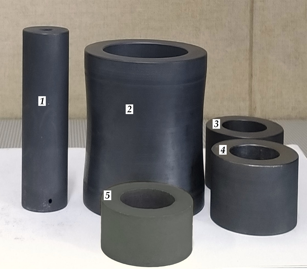
  • The central graphite insert was made hollow in order to increase its electrical resistance and reduce its heat capacity;
  • The outer side of the die and the inner side of the central insert were turned to get their special geometrical profiles.
The turning increased the electrical resistance in the middle areas of the die and insert, resulting in an increased release of Joule heat in these areas. In this case, the shape and depth of turning were chosen to minimize the radial and vertical thermal gradients over the entire surface of the SPS compacts.

3.2.2. Hollow Cylindrical GZOB Ceramics Produced Using the Standard and Modernized PSs

Two samples of GZOB hollow cylindrical ceramics of the same dimensions (outer diameter D = 72 mm, inner diameter d = 47 mm, and height h = 36 mm) were obtained under the same SPS process conditions (heating rate of 50 °C/min, holding time 5 min, SPS temperatures of 1050 °C, SPS pressure of 30 MPa) using the standard PF (Figure S2 of Supplementary Materials) and the modernized PF (Figure 5 and Figure S3 of Supplementary Materials). Here and further, the GZOB ceramics sintered by using standard and modernized PFs were labeled with S-GZOB and M-GZOB, respectively.
After sintering and cooling, the S-GZOB and M-GZOB samples were taken out from the PFs and a thin layer (up to 0.5 mm) from all their surfaces, contacting with graphite foil during sintering, was removed by grinding. Next, the density values of S-GZOB and M-GZOB were measured, and then each of the samples was cut into three equal annular parts 11 mm high. The annular parts corresponding to the upper and lower regions of the ceramics were marked as S-GZOBUp (M-GZOBUp) and S-GZOBLow (M-GZOBLow), respectively, while the annular parts obtained from the middle part of the ceramics were marked as S-GZOBMid and M-GZOBMid. Then, the density of all cut parts was also measured. The density measurement results are shown in Table 1.
The relative density of the whole S-GZOB sample before cutting is 96.7%. This value is significantly less compared with the disk sample sintered at 1050C (Figure 2). Measurements of the density of annular samples S-GZOBUp, S-GZOBLow, and S-GZOBMid clearly demonstrate the non-uniformity of densification along the height of this hollow cylindrical sample. Table 1 shows that the least dense region into the S-GZOB ceramics is localized in its middle part.
Figure 6 shows the fracture surfaces observations at the inner and the outer regions of the S-GZOB_mid sample. It is obvious that the S-GZOBMid microstructure differs significantly from the microstructure of the disk samples shown in Figure 2.
In addition to the large, elongated grains connected to each other, there are many submicron grains interspersed either separately or localized in the form of clusters in numerous pores. When passing from the outer region to the inner one, an increase in the concentration of small grain clusters and an increase in the pore sizes are observed. The formation of a microstructure under high-temperature sintering in which areas of small grains surrounded by large strongly overgrown grains may be owing to an inhomogeneous thermoconductive phenomenon. XRD phase analysis revealed three phases, doped ZnO with the wurtzite structure, homologous compound Ga2ZnmOm+3, and spinel-type Ga2ZnO4, coexisting in S-GZOBMid as listed in Figure S4 of Supplementary Materials.
The inhomogeneous thermoconductivity phenomenon at the stage of high-temperature SPS holding, at which the pressed material begins to conduct current well and intensively compacts, is caused by both the nature of uniaxial pressing during SPS and thermal inhomogeneities (along the compact’s height) that occur at the stage of indirect heating of the pressed material by the PF’s elements. This is indicated by the density measurements of samples S-GZOBUp, S-GZOBLow, and S-GZOBMid. In turn, the differences observed in the microstructure in two areas of sample A (Figure 5) indicate the presence of radial thermal inhomogeneity because SPS is a superfast process.
Thus, the studies have confirmed that the densification and sintering processes during SPS using the standard PF in the middle part of the cylindrical hollow sample having an aspect ratio h/∆r ≅ 3 (h and ∆r are the height and wall thickness of the hollow cylinder) occurred under conditions very different from the case of sintering a disk-shaped sample.
From Table 1 it can be seen that the performed geometric optimization of the die and insert design results in minimization of both the thermal inhomogeneities phenomenon and the effect of wall friction. The sample M-GZOB, obtained using the modernized PF, shows high relative density of 98.8% and good density uniformity along the height since the difference in density values of the annular samples cut from it is minimal. SEM data also confirm the high uniformity of M-GZOB both along its height and along the radial direction (Figure 7).
The appearance of grains and pores and the ratio of their number are approximately the same on the fracture surfaces of M-GZOBUp, M-GZOBLow, and M-GZOBMid. XRD studies also confirmed the high uniformity of sintered M-GZOB along its height and the coexistence of only two phases, the ZnO:Ga wurtzite phase and the homologous compound Ga2ZnmOm+3 (Figure S5 of Supplementary Materials). The spinel phase, which is a sign of thermal inhomogeneities, was absent on the patterns of M-GZOBUp, M-GZOBLow, and M-GZOBMid.
Thus, the performed geometric optimization of the design of the die and insert, aimed at reducing the cross sections in the middle parts of these PFs’ elements, makes it possible to minimize heating inhomogeneities of the molded ceramics at the initial temperature rise stage of SPS and, therefore, improves the uniformity of the resulting ceramics.

4. Conclusions

Spark plasma sintering is an available method in the synthesis of high-density doped ZnO ceramics. During the study of the SPS process of disk-shaped ceramic samples, the process temperature was optimized to obtain high-density GZOB ceramics with a uniform distribution of the Ga donor impurity. The highest relative density of 99.2% was obtained on the disk-shaped GZOB ceramic by SPS synthesis at 1050 °C. At this SPS temperature, the efficient distribution of Ga dopant ions into ZnO host was achieved through the formation of the non-spinel homologous phase Ga2ZnmOm+3 (m >> 1).
The issues associated with SPS formation of ceramics of such a complex shape as a hollow cylinder with an apex ratio h//∆r ≅ 3 (h and ∆r are the height and thickness of the cylinder wall, respectively) are considered. A geometric optimization of the design of a graphite press-form destined for the SPS formation of hollow cylindrical ceramics with a height h of 36 mm, an outer diameter D of 72 mm, and a wall thickness ∆r of 12 mm was performed. As a result of the geometric optimization of the press-form’s design, the hollow cylindrical GZOB ceramics with 98.8% density and high structural uniformity both in height and in the radial plane was achieved.
The results obtained in this study, in our opinion, revealed the possibility of their further adaptation to the task of fabricating high-quality segmented ZnO-based TCO tube targets by the energy efficient SPS method for the TCO thin film industry.

Supplementary Materials

The following supporting information can be downloaded at: https://www.mdpi.com/article/10.3390/ceramics6030080/s1, Figure S1: The digital photograph of initial ZnO powder and GZOB granular mixture prepared for SPS molding; Figure S2: Design of a standard graphite PF for SPS compacting of hollow cylindrical specimens; Figure S3: The digital photo of the PF subjected to geometric optimization and GZOB ceramic sample obtained by using this PF; Figure S4: XRD pattern of the S-GZOBMid sample; Figure S5: XRD patterns of the of the M-GZOBUp, M-GZOBMid, and M-GZOBLow samples.

Author Contributions

Conceptualization, A.K.A. and A.S.A.; Methodology, A.K.A. and V.M.K.; Formal analysis, A.S.A.; Investigation, A.K.A., S.S.M. and A.S.A.; Resources, S.S.M. and V.M.K.; Supervision, V.M.K.; Validation, A.K.A. and V.M.K.; Visualization, A.S.A. and S.S.M.; Writing—original draft preparation, A.K.A.; Writing—review and editing, A.K.A. and A.S.A. All authors have read and agreed to the published version of the manuscript.

Funding

This work was performed within the State Assignments of Dagestan Federal Research Center of Russian Academy of Sciences (in part of ceramic sintering) and FSRC “Crystallography and Photonics” RAS (in part of structural studies of oxide ceramics) and was partly supported by the RF Ministry of Education and Higher Education (Agreement # 075-15-2021-1362).

Institutional Review Board Statement

Not applicable.

Informed Consent Statement

Not applicable.

Data Availability Statement

Data are contained within the article or Supplementary Material.

Acknowledgments

The authors are grateful for additional technical support from the Analytical Shared Research Center of Dagestan Federal Research Center of RAS and the Shared Research Center of FSRC “Crystallography and Photonics” RAS.

Conflicts of Interest

The authors declare no conflict of interest.

References

  1. Seyfert, U.; Heisig, U.; Teschner, G.; Strumpfel, J. 40 years of industrial magnetron sputtering in Europe. SVC Bull. Fall 2015, 2015, 22–26. [Google Scholar]
  2. Tietema, R. 4.21—Large-Scale Industrial Coating Applications and Systems. In Comprehensive Materials Processing; Hashmi, S., Batalha, G.F., Van Tyne, C.J., Yilbas, B., Eds.; Elsevier B.V.: Amsterdam, The Netherlands, 2014; pp. 519–561. [Google Scholar] [CrossRef]
  3. Volker, L. Challenges in the industrial deposition of transparent conductive oxide materials by reactive magnetron sputtering from rotatable targets. Thin Solid Films 2017, 634, 149–154. [Google Scholar] [CrossRef]
  4. Medvedovski, E.; Szepesi, C.J.; Yankov, O.; Olsson, M.K. Rotary ITO Ceramic Sputtering Targets for Transparent Conductive Thin Films Coating. Am. Ceram. Soc. Bull. 2008, 87, 39–42. [Google Scholar]
  5. Sarkar, J. (Ed.) Chapter 4—Sputtering Target Manufacturing. In Sputtering Materials for VLSI and Thin Film Devices; William Andrew Publishing: Norwich, NY, USA, 2014; pp. 197–289. [Google Scholar] [CrossRef]
  6. Medvedovski, E.; Alvarez, N.; Yankov, O.; Olsson, M.K. Advanced indium-tin oxide ceramics for sputtering targets. Ceram. Int. 2008, 34, 1173–1182. [Google Scholar] [CrossRef]
  7. Liu, J.; Zhang, W.; Song, D.; Ma, Q.; Zhang, L.; Zhang, H.; Ma, X.; Song, H. Comparative study of the sintering process and thin film sputtering of AZO, GZO and AGZO ceramics targets. Ceram. Int. 2014, 40, 12905–12915. [Google Scholar] [CrossRef]
  8. Kalvani, P.R.; Shapouri, S.; Jahangiri, A.R.; Jalili, Y.S. Microstructure evolution in high density AZO ceramic sputtering target fabricated via multistep sintering. Ceram. Int. 2020, 46, 5983–5992. [Google Scholar] [CrossRef]
  9. Mei, F.; Yuan, T.; Li, R.; Qin, K.; Huang, J. Improving the densification of indium tin oxide targets via secondary cold isostatic pressing and oxygen exchange treatments. Scr. Mater. 2018, 155, 109–113. [Google Scholar] [CrossRef]
  10. Gao, M.; Zhang, H.; Xie, Y.; Miao, L.; Yao, W.; Zhang, F.; Wang, T.; Zhang, H. Characteristics of ultra-high density Al:ZnO sputtering targets prepared by hot isostatic pressing. Ceram. Int. 2018, 44, 5486–5491. [Google Scholar] [CrossRef]
  11. Lee, J.-R.; Chung, T.-J.; Yang, S.-H.; Hong, G.-S.; Oh, K.-S. Prevention of tapering in the tube-shaped sputtering target via initial heat treatment under external pressure. Ceram. Int. 2015, 41, 3677–3683. [Google Scholar] [CrossRef]
  12. Kelly, J.P.; Graeve, O.A. Spark Plasma Sintering as an Approach to Manufacture Bulk Materials: Feasibility and Cost Savings. JOM 2015, 67, 29–33. [Google Scholar] [CrossRef]
  13. Guillon, O.; Gonzalez-Julian, J.; Dargatz, B.; Kessel, T.; Schierning, G.; Räthel, J.; Herrmann, M. Field-assisted sintering technology/spark plasma sintering: Mechanisms, materials, and technology developments. Adv. Eng. Mater. 2014, 16, 830–849. [Google Scholar] [CrossRef] [Green Version]
  14. Gao, L.; Li, Q.; Luan, W.; Kawaoka, H.; Sekino, T.; Niihara, K. Preparation and Electric Properties of Dense Nanocrystalline Zinc Oxide Ceramics. J. Am. Ceram. Soc. 2002, 85, 1016–1018. [Google Scholar] [CrossRef]
  15. Asvarov, A.S.; Muslimov, A.E.; Akhmedov, A.K.; Abduev, A.K.; Kanevsky, V.M. A Laboratory Apparatus for Spark Plasma Sintering of Ceramic and Composite Materials. Instrum. Exp. Tech. 2019, 62, 726–730. [Google Scholar] [CrossRef]
  16. Chen, H.; Sun, Q.; Tian, T.; Zheng, L.; Barré, M.; Monot-Laffez, I.; Makowska-Janusik, M.; Li, G.; Kassiba, A.H. Defects and microstructure of highly conducting Al-doped ZnO ceramics obtained via spark plasma sintering. J. Eur. Ceram. Soc. 2020, 40, 5529–5534. [Google Scholar] [CrossRef]
  17. Sharma, S.; Bayikadi, R.; Swaminathan, P. Spark plasma sintering route to synthesize aluminium doped zinc oxide. RSC Adv. 2016, 6, 86586. [Google Scholar] [CrossRef]
  18. Takeuchi, T.; Ishida, T.; Ichikawa, K.; Miyamoto, S.; Kawahara, M.; Kageyama, H. Rapid preparation of indium tin oxide sputtering targets by spark plasma sintering. J. Mater. Sci. Lett. 2002, 21, 855–857. [Google Scholar] [CrossRef]
  19. Akhmedov, A.; Abduev, A.; Murliev, E.; Asvarov, A.; Muslimov, A.; Kanevsky, V. The ZnO-In2O3 Oxide System as a Material for Low-Temperature Deposition of Transparent Electrodes. Materials 2021, 14, 6859. [Google Scholar] [CrossRef]
  20. Ma, N.; Li, J.-F.; Zhang, B.P.; Lin, Y.H.; Ren, L.R.; Chen, G.F. Microstructure and thermoelectric properties of Zn1−xAlxO ceramics fabricated by spark plasma sintering. J. Phys. Chem. Solids 2010, 71, 1344–1349. [Google Scholar] [CrossRef]
  21. Kunikata, T.; Kato, T.; Shiratori, D.; Kantuptim, P.; Nakauchi, D.; Kawaguchi, N.; Yanagida, T. Annealing Temperature Dependence of Scintillation Properties of Ga-doped ZnO Translucent Ceramics. Sens. Mater. 2023, 35, 491–497. [Google Scholar] [CrossRef]
  22. Giuntini, D.; Raethel, J.; Herrmann, M.; Michaelis, A.; Haines, C.D.; Olevsky, E.A. Spark plasma sintering novel tooling design: Temperature uniformization during consolidation of silicon nitride powder. J. Ceram. Soc. Jpn. 2016, 124, 403–414. [Google Scholar] [CrossRef] [Green Version]
  23. Abduev, A.K.; Akhmedov, A.K.; Asvarov, A.S. The structural and electrical properties of Ga-doped ZnO and Ga, B-codoped ZnO thin films: The effects of additional boron impurity. Sol. Energy Mater. Sol. Cells 2007, 91, 258–260. [Google Scholar] [CrossRef]
  24. Abduev, A.K.; Asvarov, A.S.; Akhmedov, A.K.; Kamilov, I.K. Ceramic Target, Film Consisting of Zinc Oxide, Gallium and Boron, and Method for Preparing the Film. U.S. Patent 20,080,283,802, 20 November 2008. [Google Scholar]
  25. Pretorius, F.; Focke, W.W.; Androsch, R.; Du Toit, E. Estimating binary liquid composition from density and refractive index measurements: A comprehensive review of mixing rules. J. Mol. Liq. 2021, 332, 115893. [Google Scholar] [CrossRef]
  26. Colibaba, G.V.; Rusnac, D.; Fedorov, V.; Petrenko, P.; Monaico, E.V. Low-temperature sintering of highly conductive ZnO:Ga:Cl ceramics by means of chemical vapor transport. J. Eur. Ceram. Soc. 2021, 41, 443–450. [Google Scholar] [CrossRef]
  27. Zheng, L.; Liu, M.; Zhang, H.; Zheng, Z.; Wang, Z.; Cheng, H.; Wang, P.; Liu, Y.; Huang, B. Fabrication of ZnO Ceramics with Defects by Spark Plasma Sintering Method and Investigations of Their Photoelectrochemical Properties. Nanomaterials 2021, 11, 2506. [Google Scholar] [CrossRef] [PubMed]
  28. Liu, C.P.; Jeng, G.R. Properties of aluminum doped zinc oxide materials and sputtering thin films. J. Alloys Compd. 2009, 468, 343–349. [Google Scholar] [CrossRef]
  29. Jayathilake, D.S.Y.; Peiris, T.A.N.; Sagu, J.S.; Potter, D.B.; Wijayantha, K.G.U.; Carmalt, C.J.; Southee, D.J. Microwave-Assisted Synthesis and Processing of Al-Doped, Ga-Doped, and Al, Ga Codoped ZnO for the Pursuit of Optimal Conductivity for Transparent Conducting Film Fabrication. ACS Sustain. Chem. Eng. 2017, 5, 4820–4829. [Google Scholar] [CrossRef] [Green Version]
  30. Jood, P.; Peleckis, G.; Wang, X.; Dou, S. Effect of gallium doping and ball milling process on the thermoelectric performance of n-type ZnO. J. Mater. Res. 2012, 27, 2278–2285. [Google Scholar] [CrossRef] [Green Version]
  31. Asvarov, A.S.; Abduev, A.K.; Akhmedov, A.K.; Muslimov, A.E.; Kanevsky, V.M. On the Synthesis of ZnO: Al Ceramics by the Slip Casting Method. J. Surf. Investig. 2022, 16, 997–1002. [Google Scholar] [CrossRef]
  32. Alvarez -Ruiz, D.T.; Azough, F.; Hernandez-Maldonado, D.; Kepaptsoglou, D.M.; Ramasse, Q.M.; Day, S.J.; Svec, P.; Svec, P.S.; Freer, R. Utilising unit-cell twinning operators to reduce lattice thermal conductivity in modular structures: Structure and thermoelectric properties of Ga2O3(ZnO)9. J. Alloys Compd. 2018, 762, 892–900. [Google Scholar] [CrossRef]
  33. Chernenko, K.A.; Gorokhova, E.I.; Eronko, S.B.; Sandulenko, A.V.; Venevtsev, I.D.; Wieczorek, H. Structural, Optical, and Luminescent Properties of ZnO:Ga and ZnO:In Ceramics. IEEE Trans. Nucl. Sci. 2018, 65, 2196–2202. [Google Scholar] [CrossRef]
  34. Pham, A.T.T.; Luu, T.A.; Pham, N.K.; Ta, H.K.T.; Nguyen, T.H.; Van Hoang, D.; Phan, T.B. Multi-scale defects in ZnO thermoelectric ceramic materials co-doped with In and Ga. Ceram. Int. 2020, 46, 10748–10758. [Google Scholar] [CrossRef]
  35. Wu, M.-W.; Lai, P.-H.; Hong, C.-H.; Chou, F.-C. The sintering behavior, microstructure, and electrical properties of gallium-doped zinc oxide ceramic targets. J. Eur. Ceram. Soc. 2014, 34, 3715–3722. [Google Scholar] [CrossRef]
  36. Michiue, Y.; Mori, T. Identification of a secondary phase Ga2O3(ZnO)m in Ga-doped ZnO thermoelectric materials by a (3 + 1)-dimensional superspace model. J. Appl. Cryst. 2018, 51, 924–927. [Google Scholar] [CrossRef]
  37. Michiue, Y.; Kimizuka, N.; Kanke, Y. Structure of Ga2O3(ZnO)6: A member of the homologous series Ga2O3(ZnO)m. Acta Cryst. 2008, B64, 521–526. [Google Scholar] [CrossRef] [PubMed]
  38. Alvarez-Ruiz, D.T.; Azough, F.; Slater, T.; Day, S.J.; Freer, R. The effect of nano-twins on the thermoelectric properties of Ga2O3(ZnO)m (m = 9, 11, 13 and 15) homologous compounds. J. Eur. Ceram. Soc. 2020, 40, 5549–5558. [Google Scholar] [CrossRef]
Figure 1. The digital photographs of five disk-shaped GZOB ceramics with a diameter of 38 mm prepared at different TSPS.
Ceramics 06 00080 g001
Figure 2. Densification curve of the GZOB ceramics sintered by SPS.
Ceramics 06 00080 g002
Figure 3. SEM images of the GZOB ceramics obtained at deferent TSPS.
Ceramics 06 00080 g003
Figure 4. XRD patterns of the GZOB ceramics obtained at deferent TSPS.
Ceramics 06 00080 g004
Figure 5. Design of the modernized graphite PF for SPS compacting of hollow cylindrical specimens (1—die; 2—lower annular punch; 3—upper annular punch; 4—central hollow insert; 5—compacted powder sample; 6—lower stock of the SPS setup; 7—guide pin; 8 and 13—heat-insulating graphite foil (GRAFLEX) gaskets; 9 and 12—protective graphite foil sleeves; 10 and 11—protective graphite foil ring gaskets; 14—upper stock of the SPS setup).
Ceramics 06 00080 g005
Figure 6. SEM images of the fracture surfaces at the inner and the outer regions (according to the insets) of the S-GZOBMid sample.
Ceramics 06 00080 g006
Figure 7. SEM images of the fracture surfaces at the inner and the outer regions of the M-GZOBUp, M-GZOBMid, and M-GZOBLow samples.
Ceramics 06 00080 g007
Table 1. The relative density of the GZOB hollow cylindrical ceramics.
Sample Relative   Density   ρ % Samples after Cutting Relative   Density   ρ %
S-GZOB96.7%S-GZOBUp97.8%
S-GZOBMid94.9%
S-GZOBLow97.4%
M-GZOB98.8%M-GZOBUp98.9%
M-GZOBMid99.0%
M-GZOBLow98.6%
Disclaimer/Publisher’s Note: The statements, opinions and data contained in all publications are solely those of the individual author(s) and contributor(s) and not of MDPI and/or the editor(s). MDPI and/or the editor(s) disclaim responsibility for any injury to people or property resulting from any ideas, methods, instructions or products referred to in the content.

