Article

Effects of the Processing Technology of CVD-ZnSe, Cr2+:ZnSe, and Fe2+:ZnSe Polycrystalline Optical Elements on the Damage Threshold Induced by a Repetitively Pulsed Laser at 2.1 µm

1
Institute of Applied Physics of the Russian Academy of Sciences, 603950 Nizhny Novgorod, Russia
2
Laboratory for Radiophysical and Optical Methods of Environmental Studies, National Research Tomsk State University, 634050 Tomsk, Russia
3
Institute of Chemistry of High-Purity Substances of the Russian Academy of Sciences, 603951 Nizhny Novgorod, Russia
4
Department of Materials Science, Nizhny Novgorod State Technical University, 603950 Nizhny Novgorod, Russia
*
Author to whom correspondence should be addressed.
Ceramics 2022, 5(3), 459-471; https://doi.org/10.3390/ceramics5030035
Submission received: 14 July 2022 / Revised: 16 August 2022 / Accepted: 18 August 2022 / Published: 20 August 2022
(This article belongs to the Special Issue Advances in Ceramics)

Abstract

:
Polycrystalline zinc selenide (ZnSe) and Cr2+ or Fe2+ doped ZnSe are key optical elements in mid-infrared laser systems. The laser-induced damage of the optical elements is the limiting factor for increasing the power and pulse energy of the lasers. In the present work, the optical damage of the ZnSe, Cr2+:ZnSe, and Fe2+:ZnSe samples induced by a repetitively pulsed Ho3+:YAG laser at 2091 nm was studied. The probability of the optical damage and the laser-induced damage threshold (LIDT) were determined for the samples manufactured using different processing techniques. The highest LIDT was found in ZnSe samples annealed in an argon atmosphere. It was also found that the samples annealed in a zinc atmosphere or with hot isostatic pressing resulted in a decrease in the LIDT. The Cr2+-doped ZnSe had the lowest LIDT at 2.1 µm compared to Fe2+-doped or undoped ZnSe. The LIDT fluence of all tested ZnSe samples decreased with the increase in the pulse repetition rate and the exposure duration. The results obtained may be used to improve the treatment procedures of ZnSe, Cr2+:ZnSe, and Fe2+:ZnSe polycrystals to further increase their LIDT.

1. Introduction

Optical elements manufactured from zinc selenide (ZnSe) and Cr2+- or Fe2+-doped ZnSe are widely used in mid-infrared (mid-IR) laser systems [1,2]. ZnSe is an A2B6 direct-gap semiconductor; it has a high electrical resistivity of 1012 Ω·cm due to the large band gap of 2.7 eV at 25 °C [3]. The combination of favorable optical, physical, and chemical properties, such as high thermal conductivity, sufficient mechanical strength, chemical stability, and a wide transmittance band from the visible to the far infrared wavelength range (0.5–22 μm), have led to broad use of this material in optoelectronic devices [4]. ZnSe is used for transmission optics for CO2 lasers, acousto-optical modulators, protective windows on night vision devices, and optical elements of other equipment operating in the infrared range, in the form of windows, lenses, mirrors, prisms, beam splitters, etc. [4]. Zinc selenide is also a suitable matrix for doping with transition metal ions, in particular chromium (Cr2+) or iron (Fe2+) [2]. Such materials are active media for tunable lasers in the mid-IR wavelength range (2–5 µm) [2]. Lasers based on Cr2+:ZnSe or Fe2+:ZnSe are simple in design, compact, have a wide continuous tuning range (more than 1 μm), and can operate at room temperatures with high efficiency [5].
Many material properties depend on the method used to produce them, significantly affecting their impurity composition, inclusions, the structure of point and volume microdefects, and their concentration [4]. ZnSe production methods include the hot pressing of powder, physical vapor deposition (PVD), chemical vapor deposition (CVD), and melt growth [4]. Zinc selenide produced by the CVD method is the most widely used for optical applications [4]. It is based on the reaction of zinc vapor with hydrogen selenide at about 650–750 °C. ZnSe is deposited onto the substrate, and hydrogen is continuously pumped out of the reaction zone together with the carrier gas. The resulting material has a polycrystalline structure with a typical average grain size of about 30–50 µm. Such material has few defects and high chemical purity due to its low growth temperature (less than half the melting point of ZnSe), and a series of physical and chemical transformations leading to very effective purification from most impurities. This leads to the high optical quality of the material and, in particular, a high laser-induced damage threshold (LIDT). For example, at a wavelength of 10.6 μm when exposed to a pulsed CO2 laser, CVD-ZnSe shows the best results among other optical materials transparent in this area [6].
The laser-induced damage of the optical elements is the limiting factor for increasing the power and pulse energy of the laser systems [7,8]. The problem of the laser-induced damage of ZnSe or Cr2+:ZnSe elements has been previously discussed in several papers [9,10,11,12,13,14,15]. For infrared applications, the optical damage of the ZnSe materials at 10.6 µm has been widely studied [9,11,12,13]. In recent years, the development of solid-state lasers based on Cr2+:ZnSe or Fe2+:ZnSe crystals has stimulated interest in the optical damage of these materials under the action of CW and repetitively pulsed radiation at 2–5 μm [5,15,16]. The effects of antireflection coating or microstructures fabricated on surfaces of the ZnSe and Cr2+:ZnSe polycrystalline elements on the LIDT under laser irradiation at 2–5 µm have been examined [14,15,16]. Despite a number of previous works, the origin and mechanisms of the damage of the ZnSe, Cr2+:ZnSe, or Fe2+:ZnSe elements induced by the mid-IR laser radiation, especially in repetitively pulsed operational regimes, remain not fully understood.
This paper is focused on evaluating the optical damage of optical elements from CVD-ZnSe, Cr2+:ZnSe, or Fe2+:ZnSe polycrystals with different processing technologies induced by the repetitively pulsed Ho3+:YAG laser at 2091 nm. The effects of annealing temperature and atmosphere (containing metallic zinc, elemental selenium, or argon), the manufacture of the initial ZnSe crystals, or the experimental conditions (pulse repetition rate or exposure duration) on the LIDT were studied.

2. Materials: ZnSe, Cr2+:ZnSe and Fe2+:ZnSe

The ZnSe, Cr2+:ZnSe, and Fe2+:ZnSe elements were 15 × 10 × 3 mm3 parallelepipeds whose 10 × 15 mm2 planes were polished to III grades of finish according to GOST 11141-84 (approximately equivalent to 40/20 by MIL-O-13830A surface quality standard). The initial material for the samples was laser-quality CVD-ZnSe manufactured by INOPTICS (Nizhny Novgorod, Russia). The doping of samples with chromium (Cr2+) or iron (Fe2+) was carried out by diffusion at elevated temperature from the corresponding metal film deposited on the surface of the element. A detailed description of the procedure can be found in [17]. The samples were then sealed in vacuumed quartz ampoules containing metallic zinc (Zn), elemental selenium (Se), or argon (Ar). The amounts of the components were chosen so that at the temperature of the subsequent annealing, the pressure in the ampoule was approximately equal to 0.1 MPa. Annealing was carried out for 24 h at 1050 °C. Sample labeling includes the doping element and the atmosphere in which the annealing was performed (e.g., Cr:ZnSe_Se) or indicates that the material is original from the manufacturer and untreated (ZnSe_org). Two ZnSe samples were subjected to hot isostatic pressing (HIP). Custom-built HIP equipment UGL-2000 with a graphite heater was used. Samples were treated simultaneously in one process in graphite containers placed in different temperature zones: 900 °C and 1200 °C. The temperature was controlled by the C-type thermocouples; the argon pressure was 100 MPa and the holding time was 24 h. The ZnSe elements after the HIP were labeled as ZnSe_HIP_900 and ZnSe_HIP_1200, where the numbers correspond to the processing temperature: 900 °C or 1200 °C, respectively. The surface damage was also studied on the original polycrystalline CVD-ZnSe manufactured by PromLab LLC (Nizhny Novgorod, Russia) or II-VI Incorporation (Saxonburg, PA, USA).

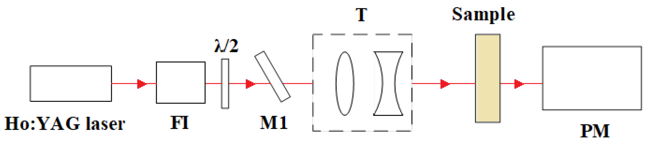
3. Experimental Setup

The experimental schematic for the optical damage tests included the following elements: a Ho3+:YAG laser with a radiation wavelength of 2091 nm; a Faraday isolator (FI); a half-wave plate (λ/2); a polarizing mirror with high transmission in p-polarization and high reflection in s- polarization (M1); a Galilean two-lens telescope (T); the tested sample (Sample); and a power meter (Coherent PM 10 with FieldMaxII detector) (Figure 1). The choice of the Ho3+:YAG laser was due to its use as a pump source of the Cr2+:ZnSe amplifiers [5]. The Ho3+:YAG laser (made in IAP RAS [18]) was pumped by a Tm-doped fiber laser at 1908 nm and was actively Q-switched by a quartz acousto-optical modulator. The beam quality parameter of the Ho3+:YAG laser was M2 < 1.2. The Q-switched laser operated with a pulse repetition rate (PRR), f, varied from 12 to 50 kHz; the FWHM pulse width (τ), 18–50 ns, depended on the PRR. The exposure duration (τexp) was varied.
The linearly polarized beam at 2091 nm was focused on the surface of the tested samples using the Galilean two-lens telescope. The beam diameter on the surface (measured by the “knife-edge” method [19]) was estimated as 0.27 mm at the e−2 intensity. The Ho3+:YAG laser power was fixed, but the power used for the tests was varied by an attenuator consisting of the half-wave plate (λ/2) and the polarizing mirror (M1) at a 55-degree angle with respect to the incident beam. The tested plates were placed behind the focus of the telescope on a three-coordinate translation stage. To avoid an influence of a backward reflection on the Ho3+:YAG laser, the Faraday isolator was used, and additionally, the input surface of the tested sample was rotated at a 3-degree angle with respect to the incident beam direction.

4. LIDT Test Method

The optical damage of the samples was studied by an “R-on-1” procedure [18,20,21,22]. In the procedure, an area on the tested surface was irradiated during a fixed exposure duration and under the same fluence of the pumping beam at each pulse of 0.1 J/cm2; if optical damage was not registered, the fluence of the site irradiation was increased step-by-step (with the step of 0.2 J/cm2) until optical damage registration. The optical damage indicators were a decrease in the sample transmission and a visible luminescence from the irradiated area. Each tested site gives a value for the damage threshold. The time interval between the tests was 2 min. It was estimated to be sufficient for the relaxations of a laser-induced heat and free-carrier electronic effect in the irradiated area. Then, the sample was moved by the plane translation to the spacing of ~0.8 mm to a new site, and the irradiation of the new site was repeated until causing damage. The number of the independent irradiated sites was NR = 5; it determined the LIDT statistic accuracy.
The damage probability dependence was obtained by plotting the cumulative probability as a function of the incident fluence. The LDT value (W0d) was taken to be the fluence, corresponding to the linear approximation of the damage probability to zero. The average LIDT fluence, Wav, and the average quadratic error, < Δ W av 2 >, were estimated from the test data by the following expressions:
W av = W i n i N
Δ W av 2 = ( W av W i ) 2 n i N ( N 1 )
where nj is the site number with the damage threshold, Wj, and N is the total number of damaged sites ( N = j n j ).
The Student’s t-distribution for the confidence probability (F(K,N)) of the damage threshold Wav to be in a mean confidence interval Wav ± K × < Δ W av 2 > was used to estimate the variable K parameter [23,24]:
F ( K , N ) = Γ ( N 2 ) π ( N 1 ) Γ [ ( N 1 ) 2 ]   K K ( 1 + z 2 N 1 ) N / 2 d z ,
where Γ is the gamma function.

5. Results

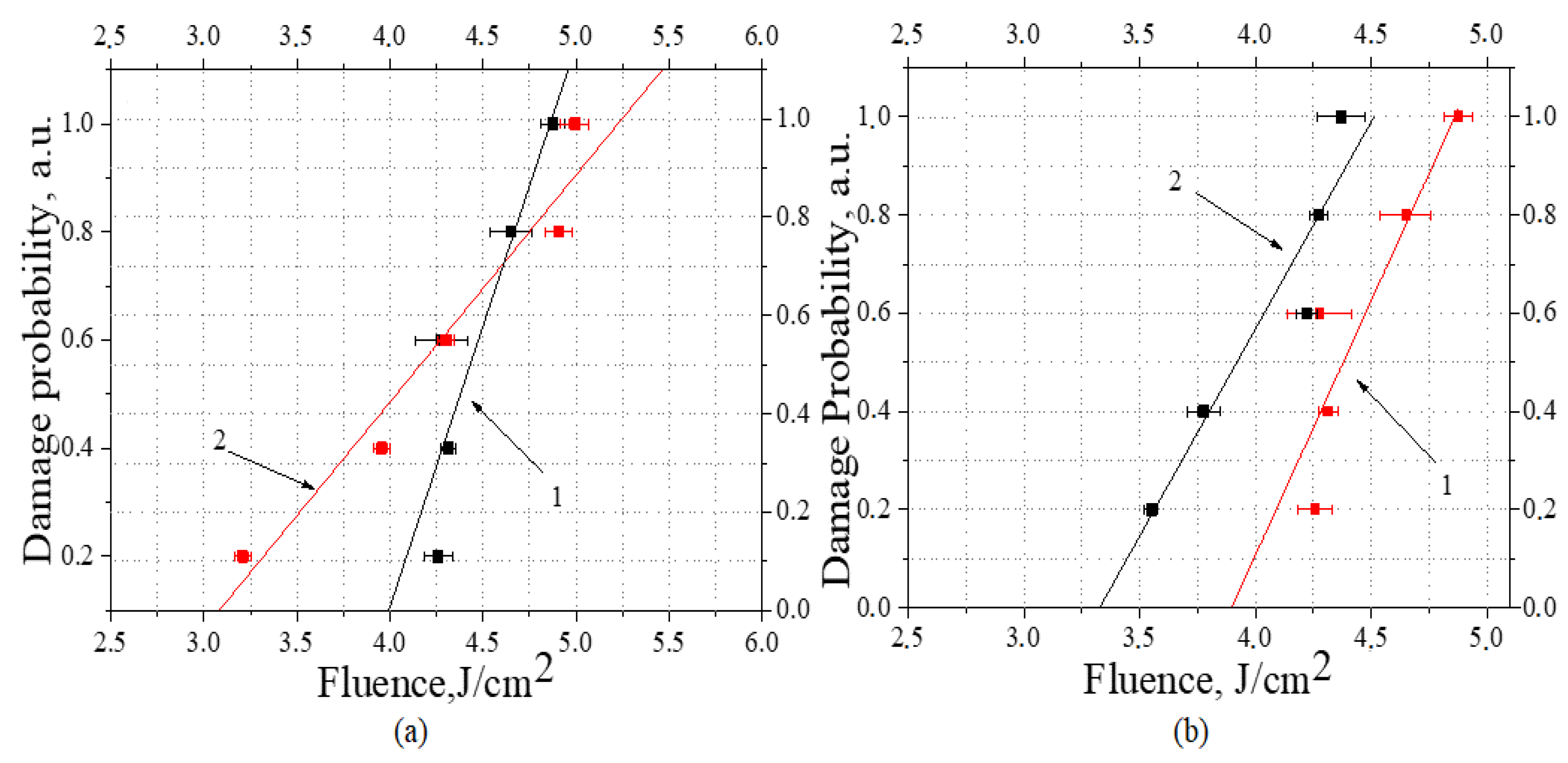
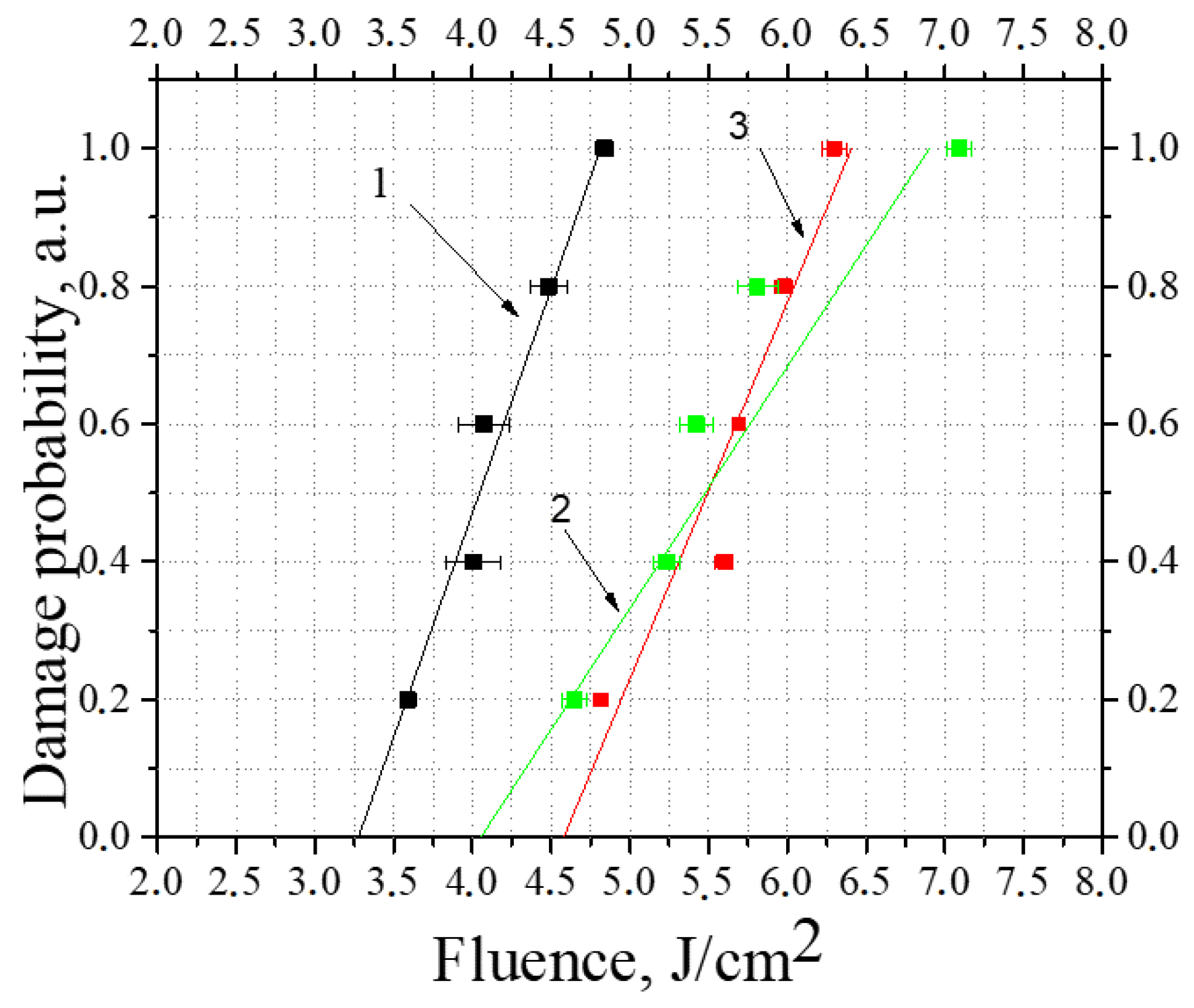
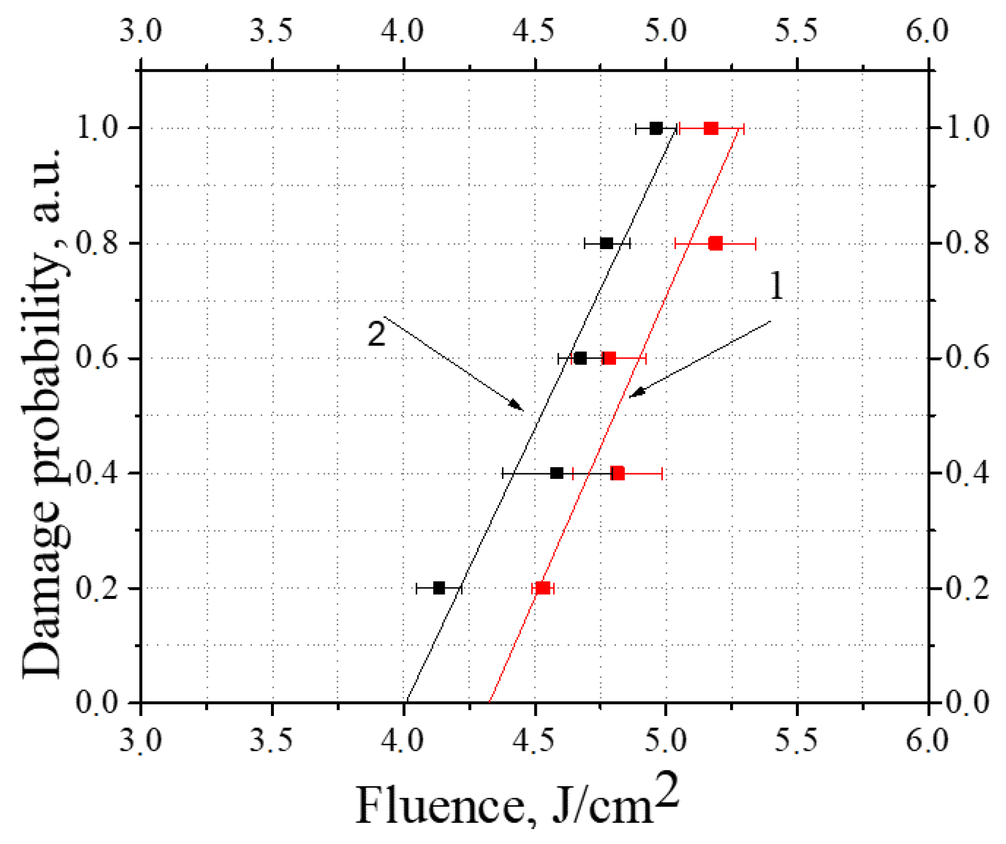
5.1. Optical Damage of ZnSe

The optical damage was registered in all irradiated ZnSe samples. The optical damage was initiated on the output surface of the plates. The probability of the optical damage for the ZnSe samples was measured and determined for the varied annealing atmosphere and temperature, technological history, PRR, and exposure duration (Figure 2, Figure 3, Figure 4, Figure 5 and Figure 6); the statistical parameters of the optical damage were estimated (Table 1 and Table 2).
Figure 2 shows the probability of the optical damage and the LIDT of the ZnSe samples (manufactured by INOPTICS) annealed in different atmospheres (Zn, Se, and Ar) in the quartz ampoule. The highest zero-probability LIDT (W0d ≈ 4.45 J/cm2) had the ZnSe sample annealed in the Ar atmosphere (ZnSe_Ar). The highest average LIDT had the ZnSe_Ar sample (Wav ≈ 4.89 J/cm2) and the ZnSe_Se sample (Wav ≈ 4.9 J/cm2) (Table 1).
An effect of the HIP treatment temperature on the LIDT was examined. The ZnSe sample HIPed at the higher temperature of 1200 °C had almost twice the LIDT of the ZnSe sample, treated at the lower temperature of 900 °C (Figure 3). Note that the HIPed materials had the lower LIDT in comparison to an initial sample ZnSe_org (compare the LIDT fluencies in Figure 2 and Figure 3).
Figure 4 demonstrates the tested LIDT of the samples from the original polycrystalline CVD-ZnSe manufactured by the different companies. The higher LIDT had the materials manufactured by PromLab LLC (line 2) and II-VI Incorporation (line 3). The higher LIDT dispersion of the ZnSe manufactured by PromLab LLC in comparison with the II-VI-manufactured ZnSe can be explained by the different inhomogeneity of the materials. The studied PromLab material has a 50% larger average grain size of 61 µm compared to the II-VI one of 40 µm. Shown in the Supplementary Materials are the images of the original ZnSe samples from different manufacturers after polishing and etching. Various studies have shown that in CVD-ZnSe, both impurity ions and inclusions are predominantly located along grain boundaries [3,25]. The original CVD-ZnSe manufactured by INOPTICS had the lower LIDT; however, after annealing in argon it had almost the same high zero-probability LIDT as materials from other manufacturers (as shown in Figure 2).
The effects of the laser characteristics on the ZnSe LIDT were studied. An influence of the exposure duration on the LIDT was studied for the ZnSe_Ar sample (Figure 5). An increase in the exposure duration at the same PRR led to the zero-probability LIDT decrease.
An influence of the PRR on the LIDT at the same exposure duration was studied for the ZnSe_Ar sample. An increase in the PRR led to the LIDT decrease (Figure 6 and Table 2).
Note that the LIDT decrease with the PRR increase had different values for the different ZnSe materials (Table 2). The determined W0d LIDT of the ZnSe_org sample decreased by 17% (on 0.6 J/cm2) at the PRR increase from 12 kHz to 16 kHz. The W0d LIDT of the ZnSe_Se and ZnSe_Ar samples decreased for 18% (on 0.7 J/cm2) or 5% (on 0.25 J/cm2), respectively, with the same PRR increase.
The following effect was found in the ZnSe samples with a W0d LIDT of more than 3 J/cm2. At an average power, close to the power at which optical damage to the material was observed, a red glow appeared (Figure 7). The laser average power, at which the glow was observed, was 250–500 mW less than the LIDT power. When the laser was switched off, the glow faded; no damage was found on the surface and in the bulk of the material. Upon the repeated irradiation of the sample, the glow appeared again. The glow effect was observed in all tested samples, independent of the treatment procedures. Similar red luminescence in ZnSe induced by X-ray or visible light or even caused by thermal excitation was recently reported [26,27,28,29]. The luminescence may be explained by the radiative recombination of free electrons with holes localized on the oxygen-related defect centers of the chalcogenides [27,28,29].

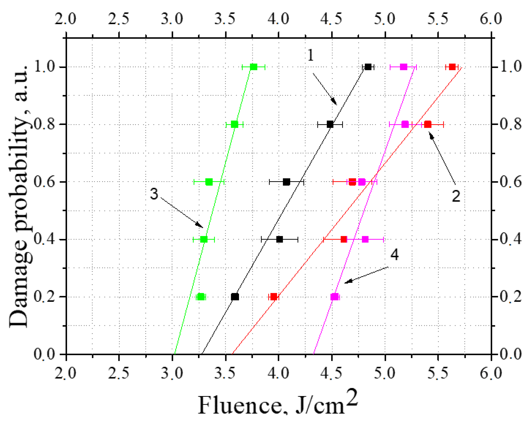
5.2. Optical Damage of Cr2+:ZnSe and Fe2+:ZnSe

The optical damage of the ZnSe materials doped by Cr2+ or Fe2+ ions was studied. One surface of the Cr2+:ZnSe and Fe2+:ZnSe plates was antireflection-coated (at 2.1 µm) by a dielectric film formed by ZnS and YF3 layers. The optical damage was initiated on the output surface of the plates independent of the antireflection coating.
The probability of the optical damage of the Cr2+:ZnSe_Ar and Fe2+:ZnSe_Ar samples in comparison with the ZnSe_Ar sample was measured (Figure 8). The zero-probability and average LIDTs were determined (Table 3). The Cr2+-doped sample had the lowest LIDTs due to a strong absorption at 2.1 µm: the absorption cross-section of the Cr2+:ZnSe at 2091 nm is σabs ≈ 1.4 × 10⁻¹⁹ cm2 [2,5]. The strong LIDT decrease in the Cr2+:ZnSe_Se sample in comparison with the ZnSe_Se sample was also registered (compare Table 2 and Table 3). However, the LIDTs of the Cr2+:ZnSe_Zn, Cr2+:ZnSe_Ar and the ZnSe_Zn sample were comparable. The Fe2+-doped sample Fe2+:ZnSe_Ar had the lower LIDT in comparison with ZnSe_Ar, but the higher LIDT in comparison with Cr2+:ZnSe_Ar. This fact can be explained by the absorption of the Fe2+ ions at 2091 nm [30] and a higher probability of oxygen contamination of the samples during the longer annealing procedure of the Fe2+ doping.
The LIDT of the Fe2+:ZnSe_Ar decreased with the PRR increase at the constant exposure duration (Figure 9a), or with the exposure duration increase at the constant PRR (Figure 9b).

6. Discussion

The region of existence of ZnSe-Zn or ZnSe-Se solid solutions is known to be extremely small: on the order of 10−6 mol of excess Zn or Se [31]. For this reason, when the material is produced by chemical vapor deposition, deviations from the stoichiometry of the components supplied to the reactor form their inclusions in the material in elemental form. Since the presence of Zn inclusions has the greatest effect on radiation absorption, ZnSe growth tends to proceed in a small excess of selenium [32]. However, the unstable gas dynamics in the CVD reactor do not allow the complete prevention of local fluctuations of components and the formation of inclusions of both elements. Probably, the difference in the LIDT results of ZnSe from different manufacturers (Figure 4) is related to the accuracy of gas flow control and, consequently, to the unequal number of such inclusions. To our knowledge, the three manufacturers of the tested materials are the largest in the world and have reactors of tonnage capacity. The range of conditions under which it is possible to obtain laser-quality material in large reactors is quite narrow, so we assume that the other ZnSe parameters that could affect the optical breakdown threshold (e.g., impurity composition) are close in all the manufacturers considered.
Annealing in Zn or Se vapor causes them to fill the pores inevitably present in the material, as well as enriching the ZnSe matrix with the corresponding component. As the temperature decreases, they condense in the pores, and their solubility in the matrix decreases, which leads to the formation of elemental inclusions in the volume of the material. This explains well the dependences observed in Figure 2.
ZnSe annealed in a zinc atmosphere has the highest absorption and therefore has the lowest LIDT. In the original ZnSe (manufactured by INOPTICS), the absorption also appears to be largely due to zinc inclusions, but which are much smaller than in the ZnSe_Zn sample. Annealing in selenium vapor removes all zinc inclusions. Since elemental selenium is transparent to radiation at 2091 nm, the LIDT in the ZnSe_Se sample is higher than in the original ZnSe. The sample annealed in argon has the highest zero-probability LIDT. This annealing allows the interaction reactions of elemental Zn and Se to complete, and the excess component evaporates from the sample, forming the most stoichiometric material with the fewest inclusions. Such a material has almost the same LIDT as ZnSe with the initially high breakdown threshold produced by II-VI and PromLab. However, the ZnSe_Ar sample has a 100% probability of optical damage lower by 16 and 25%, respectively. It can be assumed that the origin of the defects limiting the onset of breakdown in all three materials under study is the same, but the different slope of the breakdown probability curves indicates a non-uniform distribution of such defects or a change in the damage mechanism. In favor of the latter, there are noticeable deviations of the experimental points from the approximating straight line. For example, zero-probability LIDT can limit macro defects—particles of ZnO or graphite, contamination with which is possible during material growth—and a 100% probability of optical breakdown is provided by impurity-defective centers. Annealing inevitably leads to an increase in the concentration of impurities, the most common of which is oxygen [32]. The visually-observed effect of the red glow in the ZnSe sample near the LIDT fluence can be also explained by the luminescence of the oxygen impurities.
The HIP-treated materials have a significantly lower LIDT than both the original samples and those annealed in Ar. Despite the same mechanism of Zn and Se elemental inclusions removal, the probability of impurity contamination is higher under HIP treatment conditions [32]. This is due to the fact that the quartz ampoule for annealing is easy enough to clean. The sample is in contact with only a few tens of ml of argon, and the ingress of impurities from the quartz can usually be neglected, except for the oxygen impurity, which, depending on temperature and glass quality, can penetrate into the ampoule in noticeable quantities. The situation with processing in the HIP is different. The chamber in which the processing takes place contains many elements made from different materials. The complete removal of adsorbed gases (primarily water) from them is technically impossible. Even relatively small chambers contain thousands of liters of argon, and every thousand liters contains 1 mL of impurity gases when using Ar of purity 6N. Additionally, the same equipment is used to process different materials. All of the above makes it extremely difficult to maintain the initial purity of ZnSe in terms of metallic impurities during the HIP treatment, and oxygen contamination is inevitable. As shown earlier, at wavelengths less than 10 µm, absorption in CVD-ZnSe occurs on free carriers, the source of which are impurity ions [3,33]
The significantly lower LIDT of the ZnSe_HIP_900 sample in comparison with the ZnSe_HIP_1200 one can be explained by the different distribution of impurities in the volume of the samples. The movement of impurity defect centers during HIP from the surface deep into the sample was observed in [34,35]. ZnSe treated at 1200 °C for 53 h showed the most homogeneous distribution of such centers compared to samples annealed in an ampoule at 1000 °C. Increasing the homogeneity of impurity distribution during annealing can significantly reduce the absorption of free carriers [3]. At lower temperatures, much of the impurities are in the near-surface layer, which creates conditions for surface breakdown. Processing at high temperatures allows more complete diffusion processes, which, at an equal content of impurities, reduces their local concentration. This fact can also be explained by the different responses of the samples to changes in exposure duration. ZnSe_HIP_1200 had the 14% (0.5 J/cm2) LIDT increase with increasing exposure duration from 1 s to 10 s, and ZnSe_HIP_900 has 11% (0.4 J/cm2) of the LIDT decrease in the same conditions.
The zero-probability LIDT fluence of all tested ZnSe and Fe2+:ZnSe samples decreased with the increase in the PRR and the exposure duration, as shown in Figure 5, Figure 6 and Figure 9. This result appears to be in good agreement with the incubation phenomenon when the LIDT fluence decreases with the increase in the number of pulses during irradiation. This phenomenon is well known for different optical materials [7,8,24]. The incubation effect in our experiments can be explained by the temperature rise in the beam center over the exposure duration, which resulted in a higher absorption coefficient, photochemical effects, and a lower critical specific damage fluence. Note that the slope of the damage probability in ZnSe samples apparently decreased upon increasing the exposure time (Figure 5); however, this effect was absent in the Fe2+:ZnSe samples (Figure 9b). This may be explained by the additional annealing of the high-quality irradiated spot in ZnSe during long exposure, and it is not valid for the annealed Fe2+:ZnSe samples.

7. Conclusions

The optical damage probability and LIDTs of the polycrystalline ZnSe, Cr2+:ZnSe, and Fe2+:ZnSe samples, manufactured using different processing technology, were analyzed at 2.1 µm as a function of the Ho3+:YAG laser fluence. The annealing of the materials in the argon or selenium atmospheres resulted in the LIDT increasing; however, the zinc atmosphere for annealing or the HIP treatment led to the LIDT decreasing. The highest LIDT was found in the ZnSe samples annealed in an Ar atmosphere. Cr2+-doped ZnSe had the lower LIDT at 2.1 µm in comparison with the Fe2+-doped or undoped ZnSe. The LIDT fluence of all tested samples decreased with the increase in the PRR and the exposure duration of the repetitively pulsed Ho3+:YAG laser, and this can be explained by the incubation phenomenon. The results obtained serve as information for the improvement of treatment procedures for ZnSe, Cr2+:ZnSe, and Fe2+:ZnSe elements to further increase their LIDT.

Supplementary Materials

The following supporting information can be downloaded at: https://www.mdpi.com/article/10.3390/ceramics5030035/s1. Figure S1. Images of the polished and etched surfaces of the original ZnSe samples from different manufacturers: the polycrystalline ZnSe manufactured by INOPTICS, Nizhny Novgorod, Russia (a); the polycrystalline ZnSe manufactured by PromLab LLC, Nizhny Novgorod, Russia (b); the polycrystalline ZnSe manufactured by II-VI Incorporated, Saxonburg, USA (c).

Author Contributions

Conceptualization, O.A. and S.B.; methodology, N.Y., O.A. and S.B.; software, Y.G.; validation, N.Y. and I.E.; formal analysis, Y.G.; investigation, N.Y., O.A., I.E. and S.B.; resources, O.A. and S.B.; data curation, E.S.; writing—original draft preparation, Y.G. and E.S.; writing—review and editing, O.A. and S.B.; visualization, Y.G.; supervision, O.A. and S.B.; project administration, O.A.; funding acquisition, O.A. All authors have read and agreed to the published version of the manuscript.

Funding

This research was supported by the Russian Science Foundation (project No. 22-12-20035, https://rscf.ru/en/project/22-12-20035, accessed on 25 March 2022) and the Ministry of Education, Science and Youth Policy of the Nizhny Novgorod Region (agreement No. 316-06-16-17/22 accessed on 31 March 2022).

Institutional Review Board Statement

Not applicable.

Informed Consent Statement

Not applicable.

Data Availability Statement

Not applicable.

Conflicts of Interest

The authors declare no conflict of interest. The funders had no role in the design of the study; in the collection, analyses, or interpretation of data; in the writing of the manuscript, or in the decision to publish the results.

References

  1. Harris, D.C. Development of Hot-Pressed and Chemical-Vapor-Deposited Zinc Sulfide and Zinc Selenide in the United States for Optical Windows; Tustison, R.W., Ed.; SPIE: Bellingham, WA, USA, 2007; p. 654502. [Google Scholar]
  2. DeLoach, L.D.; Page, R.H.; Wilke, G.D.; Payne, S.A.; Krupke, W.F. Transition metal-doped zinc chalcogenides: Spectroscopy and laser demonstration of a new class of gain media. IEEE J. Quantum Electron. 1996, 32, 885–895. [Google Scholar] [CrossRef]
  3. Lewis, K.L.; Arthur, G.S. Surface and Free Carrier Absorption Processes in CVD Zinc Selenide. In Laser Induced Damage in Optical Materials: 1982; Bennett, H.E., Ed.; U.S. Government Printing Office Washington: Boulder, CO, USA, 1984; pp. 86–101. [Google Scholar]
  4. Gavrushchuk, E.M. Polycrystalline Zinc Selenide for IR Optical Applications. Inorg. Mater. 2003, 39, 883–899. [Google Scholar] [CrossRef]
  5. Mirov, S.B.; Moskalev, I.S.; Vasilyev, S.; Smolski, V.; Fedorov, V.V.; Martyshkin, D.; Peppers, J.; Mirov, M.; Dergachev, A.; Gapontsev, V. Frontiers of Mid-IR Lasers Based on Transition Metal Doped Chalcogenides. IEEE J. Sel. Top. Quantum Electron. 2018, 24, 1–29. [Google Scholar] [CrossRef]
  6. Taylor, R.L.; Goela, J.S. Specification Of Infrared Optical Materials For Laser Applications; Fischer, R.E., Smith, W.J., Eds.; SPIE: Bellingham, WA, USA, 1986; p. 22. [Google Scholar] [CrossRef]
  7. Ristau, D. (Ed.) Laser-Induced Damage in Optical Materials; CRC Press: Boca Raton, FL, USA, 2014; ISBN 9781439872178. [Google Scholar] [CrossRef]
  8. Manenkov, A.A.; Prokhorov, A.M. Laser-induced damage in solids. Sov. Phys. Uspekhi 1986, 29, 104–122. [Google Scholar] [CrossRef]
  9. Kovalev, V.I.; Faizullov, F.S. Investigation of surface breakdown mechanism in IR-optical materials. In Laser Induced Damage in Optical Materials; ASTM International: West Conshohocken, PA, UA, 1978; p. 318. [Google Scholar]
  10. Benson, S.; Szarmes, E.; Hooper, B.; Dottery, E.; Madey, J. Laser Damage on Zinc Selenide and Cadmium Telluride Using the Stanford Mark III Infrared Free Electron Laser. In Laser Induced Damage in Optical Materials: 1987; ASTM International: West Conshohocken, PA, USA, 1988; pp. 41–49. [Google Scholar] [CrossRef]
  11. Haas, C.R.; Kreutz, E.-W.; Wesner, D.A. Damage to Coated ZnSe Optical Components by High-Power CO2 Laser Radiation; Bennett, H.E., Chase, L.L., Guenther, A.H., Newnam, B.E., Soileau, M.J., Eds.; SPIE: Bellingham, WA, USA, 1994; p. 732. [Google Scholar] [CrossRef]
  12. Lefranc, S.; Kudriavtsev, E.M.; Autric, M.L. Pulsed-Laser-Induced Damage in Semiconductors Ge, ZnS, and ZnSe at 10.6 um; Exarhos, G.J., Guenther, A.H., Kozlowski, M.R., Soileau, M.J., Eds.; SPIE: Bellingham, WA, USA, 1998; p. 605. [Google Scholar] [CrossRef]
  13. Krol, H.; Grèzes-Besset, C.; Gallais, L.; Natoli, J.-Y.; Commandré, M. Study of Laser-Induced Damage at 2 Microns on Coated and Uncoated ZnSe Substrates; Exarhos, G.J., Guenther, A.H., Lewis, K.L., Ristau, D., Soileau, M.J., Stolz, C.J., Eds.; SPIE: Bellingham, WA, USA, 2006; p. 640316. [Google Scholar] [CrossRef]
  14. Hobbs, D.; Macleod, B.; Sabatino, E.; Mirov, S.; Martyshkin, D.; Mirov, M.; Tsoi, G.; McDaniel, S.; Cook, G. Laser testing of anti-reflection micro-structures fabricated in ZnSe and chromium-ion doped ZnSe laser gain media. Opt. Mater. Express 2017, 7, 3377. [Google Scholar] [CrossRef]
  15. Hobbs, D.S.; MacLeod, B.D.; Sabatino, E.; Mirov, S.B.; Martyshkin, D.V. Laser Damage Resistant Anti-Reflection Microstructures for Mid-Infrared Metal-Ion Doped ZnSe Gain Media; Exarhos, G.J., Gruzdev, V.E., Menapace, J.A., Ristau, D., Soileau, M.J., Eds.; SPIE: Bellingham, WA, USA, 2012; p. 85300P. [Google Scholar] [CrossRef]
  16. McDaniel, S.; Hobbs, D.; MacLeod, B.; Sabatino, E.; Berry, P.; Schepler, K.; Mitchell, W.; Cook, G. Cr:ZnSe laser incorporating anti-reflection microstructures exhibiting low-loss, damage-resistant lasing at near quantum limit efficiency. Opt. Mater. Express 2014, 4, 2225. [Google Scholar] [CrossRef]
  17. Timofeeva, N.A.; Gavrishchuk, E.M.; Savin, D.V.; Rodin, S.A.; Kurashkin, S.V.; Ikonnikov, V.B.; Tomilova, T.S. Fe2+ Diffusion in CVD ZnSe during Annealing in Different (Ar, Zn, and Se) Atmospheres. Inorg. Mater. 2019, 55, 1201–1205. [Google Scholar] [CrossRef]
  18. Yudin, N.; Antipov, O.; Eranov, I.; Gribenyukov, A.; Verozubova, G.; Lei, Z.; Zinoviev, M.; Podzvalov, S.; Slyunko, E.; Voevodin, V.; et al. Laser-Induced Damage Threshold of Single Crystal ZnGeP2 at 2.1 µm: The Effect of Crystal Lattice Quality at Various Pulse Widths and Repetition Rates. Crystals 2022, 12, 652. [Google Scholar] [CrossRef]
  19. ISO 11146-1:2021. Lasers and Laser-Related Equipment—Test Methods for Laser Beam Widths, Divergence Angles and Beam Propagation Ratios. International Organization for Standardization: Geneva, Switzerland, 2005; p. 11146-2.
  20. Hue, J.; Garrec, P.; DiJon, J.; Lyan, P. R-on-1 Automatic Mapping: A New Tool for Laser Damage Testing; Bennett, H.E., Guenther, A.H., Kozlowski, M.R., Newnam, B.E., Soileau, M.J., Eds.; SPIE: Bellingham, WA, USA, 1996; p. 90. [Google Scholar] [CrossRef]
  21. Hildenbrand, A.; Kieleck, C.; Tyazhev, A.; Marchev, G.; Stöppler, G.; Eichhorn, M.; Schunemann, P.G.; Panyutin, V.L.; Petrov, V. Laser damage of the nonlinear crystals CdSiP2 and ZnGeP2 studied with nanosecond pulses at 1064 and 2090 nm. Opt. Eng. 2014, 53, 122511. [Google Scholar] [CrossRef]
  22. Yudin, N.N.; Antipov, O.L.; Gribenyukov, A.I.; Eranov, I.D.; Podzyvalov, S.N.; Zinoviev, M.M.; Voronin, L.A.; Zhuravleva, E.V.; Zykova, M.P. Effect of postgrowth processing technology and laser radiation parameters at wavelengths of 2091 and 1064 nm on the laser-induced damage threshold in ZnGeP2 single crystal. Quantum Electron. 2021, 51, 306–316. [Google Scholar] [CrossRef]
  23. ISO 2602:1980. Statistical Interpretation of Test Results—Estimation of the Mean—Confidence Interval. International Organization for Standardization: Geneva, Switzerland, 1980.
  24. Sun, Z.; Lenzner, M.; Rudolph, W. Generic incubation law for laser damage and ablation thresholds. J. Appl. Phys. 2015, 117, 073102. [Google Scholar] [CrossRef]
  25. Chen, M.; Cui, H.; Li, W.; Kou, H.; Li, J.; Pan, Y.; Jiang, B. Reparative effect of diffusion process on host defects in Cr2+ doped ZnS/ZnSe. J. Alloys Compd. 2014, 597, 124–128. [Google Scholar] [CrossRef]
  26. Gladilin, A.A.; Chentsov, S.I.; Mironov, S.A.; Uvarov, O.V.; Ilichev, N.N.; Studenikin, M.I.; Gavrischuk, E.M.; Timofeeva, N.A.; Aminev, D.F.; Kalinushkin, V.P. Effect of Zinc Atmosphere upon Doping ZnSe: Fe Crystals on the Composition and Distribution of Impurity-Defect Centers. Bull. Lebedev Phys. Inst. 2020, 47, 237–243. [Google Scholar] [CrossRef]
  27. Morozova, N.K.; Karetnikov, I.A.; Blinov, V.V.; Gavrishchuk, E.M. A study of luminescence centers related to copper and oxygen in ZnSe. Semiconductors 2001, 35, 24–32. [Google Scholar] [CrossRef]
  28. Brodyn, M.S.; Degoda, V.Y.; Alizadeh, M.; Podust, G.P.; Pavlova, N.Y.; Kozhushko, B.V. Deep traps concentrations in ZnSe single crystals. Mater. Sci. Eng. B 2020, 258, 114570. [Google Scholar] [CrossRef]
  29. Degoda, V.Y.; Podust, G.P.; Doroshenko, I.Y.; Pavlova, N.Y. Phosphorescence and conduction current relaxation in ZnSe crystals. Opt. Mater. 2022, 129, 112460. [Google Scholar] [CrossRef]
  30. Fürtjes, P.; Tomm, J.W.; Griebner, U.; Steinmeyer, G.; Balabanov, S.S.; Gavrishchuk, E.M.; Elsaesser, T. Kinetics of excitation transfer from Cr2+ to Fe2+ ions in co-doped ZnSe. Opt. Lett. 2022, 47, 2129. [Google Scholar] [CrossRef]
  31. Hexkicberg, M.M.; Stevexsok, A. Self-diffusion of Zn and Se in ZnSe. Phys. Status Solidi 1971, 48, 255–269. [Google Scholar] [CrossRef]
  32. Mironov, E.A.; Palashov, O.V.; Balabanov, S.S. High-purity CVD-ZnSe polycrystal as a magneto-active medium for a multikilowatt Faraday isolator. Opt. Lett. 2021, 46, 2119. [Google Scholar] [CrossRef]
  33. Klein, C.A.; Miller, R.P.; Stierwalt, D.L. Surface and bulk absorption characteristics of chemically vapor-deposited zinc selenide in the infrared. Appl. Opt. 1994, 33, 4304. [Google Scholar] [CrossRef]
  34. Balabanov, S.S.; Gavrishchuk, E.M.; Gladilin, A.A.; Ikonnikov, V.B.; Il’ichev, N.N.; Kalinushkin, V.P.; Mironov, S.A.; Savin, D.V.; Studenikin, M.I.; Timofeeva, N.A.; et al. Spatial Distribution of Impurity Defect Centers in Fe-Doped Polycrystalline Zinc Selenide. Inorg. Mater. 2019, 55, 423–431. [Google Scholar] [CrossRef]
  35. Gavrishchuk, E.M.; Gladilin, A.A.; Danilov, V.P.; Ikonnikov, V.B.; Il’ichev, N.N.; Kalinushkin, V.P.; Ryabova, A.V.; Studenikin, M.I.; Timofeeva, N.A.; Uvarov, O.V.; et al. Distribution of luminescence centers in the bulk of undoped, Fe-doped, and Cr-doped CVD ZnSe polycrystals studied by two-photon confocal microscopy. Inorg. Mater. 2016, 52, 1108–1114. [Google Scholar] [CrossRef]
Figure 1. Optical layout of the experimental setup for the study of the Cr2+:ZnSe optical damage.
Ceramics 05 00035 g001
Figure 2. Damage probability vs the laser beam fluence for the ZnSe samples annealed in different atmospheres: an initial ZnSe sample without annealing, ZnSe_org (1); the ZnSe sample annealed in selenium, ZnSe_Se (2); the ZnSe sample annealed in zinc, ZnSe_Zn (3); the ZnSe sample annealed in argon, ZnSe_Ar (4). The pulse repetition rate (PRR) of the Ho3+:YAG laser was 12 kHz, the exposure duration was 1 s.
Ceramics 05 00035 g002
Figure 3. Damage probability vs the laser beam fluence for the ZnSe samples hot isostatically pressed (HIPed) at different temperatures: ZnSe_HIP_1200 (1), ZnSe_HIP_900 (2). The PRR of the Ho3+:YAG laser was 12 kHz, the exposure duration was 1 s.
Ceramics 05 00035 g003
Figure 4. Damage probability vs the laser beam fluence for the original ZnSe samples from different manufacturers: the polycrystalline ZnSe manufactured by INOPTICS, Nizhny Novgorod, Russia (1); the polycrystalline ZnSe manufactured by PromLab LLC, Nizhny Novgorod, Russia (2); the polycrystalline ZnSe manufactured by II-VI Incorporated, Saxonburg, USA (3). The PRR of the Ho3+:YAG laser was 12 kHz, the exposure duration was 1 s.
Ceramics 05 00035 g004
Figure 5. Damage probability of the ZnSe_Ar sample vs the laser beam fluence for different exposure durations of the Ho3+:YAG laser (at 16 kHz PRR): 1 s (1), 20 s (2), 40 s (3), 60 s (4).
Ceramics 05 00035 g005
Figure 6. Damage probability vs fluence for ZnSe_Ar for PRR 12 kHz (1) or 16 kHz (2). The exposure duration was 1 s.
Ceramics 05 00035 g006
Figure 7. The red glow from the laser-irradiated area of the ZnSe sample.
Ceramics 05 00035 g007
Figure 8. Damage probability vs the laser beam fluence for the samples: ZnSe_Ar (1), Fe2+:ZnSe_Ar (2), Cr2+:ZnSe_Ar (3).
Ceramics 05 00035 g008
Figure 9. Damage probability vs fluence for Fe2+:ZnSe_Ar at the varied PRR of 12 kHz (1) or 16 kHz (2) at the constant exposure duration of 1 s (a), or at the varied exposure duration of 1 s (1) or 10 s (2) at the fixed PRR of 12 kHz (b).
Ceramics 05 00035 g009
Table 1. The PRR of the laser radiation, f; the number of the damaged sites, N; the average quadratic error, < Δ W av 2  >; the K coefficient of the error dispersion at the confidence probability of F = 0.95; the average laser-induced damage threshold (LIDT) fluence, Wav; the 0-probability LIDT fluence, W0d, for the ZnSe samples with different annealing atmospheres. The exposure duration was 1 s.
Samplef, kHzNWav2 > 1/2 J/cm2KWav, J/cm2W0d, J/cm2
ZnSe_org1250.052.8(4.2 ± 0.14)(3.28 ± 0.06)
ZnSe_Se1250.092.8(4.9 ± 0.3)(3.6 ± 0.3)
ZnSe_Zn1250.012.8(3.45 ± 0.03)(3.01 ± 0.03)
ZnSe_Ar1250.022.8(4.89 ± 0.06)(4.32 ± 0.06)
Table 2. The number of the damaged sites, N; the average quadratic error, < Δ W av 2 >; the K coefficient of the error dispersion at the confidence probability of F = 0.95; the average LIDT fluence, Wav; the 0-probability LIDT fluence, W0d, for the ZnSe samples at different PRR (f) of the Ho3+:YAG laser: 12 or 16 kHz. The exposure duration was 1 s.
Samplef, kHzN<ΔWav2 > 1/2, J/cm2KWav, J/cm2W0d, J/cm2
ZnSe_Ar1250.022.8(4.89 ± 0.06)(4.32 ± 0.06)
ZnSe_Ar1650.022.8(4.63 ± 0.06)(4.01 ± 0.06)
ZnSe_org1250.022.8(4.19 ± 0.04)(3.43 ± 0.04)
ZnSe_org1650.022.8(4.46 ± 0.02)(4.044 ± 0.02)
ZnSe_Se1250.022.8(4.85 ± 0.06)(3.78 ± 0.06)
ZnSe_Se1650.022.8(4.86 ± 0.02)(4.5 ± 0.02)
ZnSe_Zn1250.022.8(3.44 ± 0.02)(3.09 ± 0.02)
ZnSe_Zn1650.022.8(3.51 ± 0.03)(2.99 ± 0.03)
Table 3. The PRR of the laser radiation, f; the number of the damaged sites, N; the average quadratic error, < Δ W av 2  >; the K coefficient of the error dispersion at the confidence probability of F = 0.95; the average LIDT fluence, Wav; the 0-probability LIDT fluence, W0d, for the ZnSe_Ar, Fe2+-, and Cr2+-doped samples. The exposure duration was 1 s.
Samplef, kHzN<ΔWav2 > 1/2, J/cm2KWD, J/cm2W0d, J/cm2
ZnSe_Ar1250.022.8(4.89 ± 0.06)(4.32 ± 0.06)
Fe2+:ZnSe_Ar1250.022.8(4.47 ± 0.06)(3.89 ± 0.06)
Cr2+:ZnSe_Ar1250.0012.8(2.658 ± 0.001)(2.577 ± 0.001)
Cr2+:ZnSe_Se1250.032.8(2.31 ± 0.03)(1.82 ± 0.08)
Cr2+:ZnSe_Zn1250.012.8(2.82 ± 0.03)(2.6 ± 0.03)
Publisher’s Note: MDPI stays neutral with regard to jurisdictional claims in published maps and institutional affiliations.

