1. Introduction
The development of advanced engineering materials with graded compositions and/or microstructures and properties, commonly known as functionally graded materials (FGMs) [
1], has experienced a continuous growth since 1990s. Graded ceramics have also shown a comparable tendency accounting for around 25% of the total number of published documents (according to the Scopus database). Ceramic FGMs display a promising range of industrial applications, including aerospace, automotive, energy production and biomedicine [
2].
One of the main challenging issues when a FGM is manufactured is to avoid, or at least to reduce, the residual stresses generated along the graded structure. One possible solution is to develop a linear thermal gradient along the powder compact by using the spark plasma sintering (SPS) technique, which leads to a continuous change of the composition and/or microstructure throughout the material [
3,
4,
5]. In this way, Hong et al. [
3] manufactured FGMs of ZrB
2–SiC/ZrO
2 composites with a layered structure by modifying the ZrO
2 content into each layer, and employing a graphite die with a tronco-conical section into the SPS furnace. As a result, the sintering temperature was lower at the bottom of the specimen than at the top, and the whole material exhibited high density with the adjacent layers firmly bonded. Another approach consisted in creating that temperature gradient into the SPS system using an asymmetric setting of the punches and die. In this sense, Hulbert et al. [
4] developed continuous B
4C/Al FGMs by partially introducing the bottom punch into the graphite die. The material showed a gradual change of hardness across the specimen. Belmonte et al. [
5] also attained a continuous variation of hardness and fracture toughness in graded Si
3N
4 ceramics processed from a sole homogeneous powder composition. In this case, the bottom punch was completely enclosed into the die and leaned on the spacer, promoting a distinct Si
3N
4 phase transformation degree and, hence, variable mechanical properties, across the ceramics. These authors further augmented that mechanical gradient by placing an electrical insulator (BN slab) between the top punch and the ceramic powder compact that produced a temperature gradient across the specimen well above of 150 °C [
6].
On the other hand, the addition of graphene-based nanostructures to ceramic matrices has enabled to produce new composites with outstanding structural and functional properties [
7,
8,
9]. In the case of Si
3N
4 ceramics, the graphene containing composites increased, for instance, the fracture toughness and the wear resistance of monolithic ceramics, or turned the electrical response from electrical insulator (monolithic) to conductor (composite).
Taking into account the interest attracted by FGMs and ceramic/graphene composites, the aim of the present work is to take one step forward and merge both strategies, i.e., to develop continuous functionally graded Si
3N
4/graphene composites. Presently, there are scarce works devoted to graphene-based FGMs, most of them focused on polymeric matrices [
10], although some studies related to WC ceramics can be found [
11,
12]. In these works, WC layers with distinct cobalt contents were stacked and liquid phase sintered. Moreover, some of those layers contained graphene nanoplatelets (GNPs), which maintained the stability of the predesigned cobalt gradient and produced graded mechanical properties. Therefore, to the best of our knowledge, this is the first time that a continuous graded Si
3N
4/graphene composite is developed. This FGM was processed in one step from a single powder composition containing graphene oxide sheets (GOs) and using the SPS technique in a similar way to a previous work [
6]. The changes in the SPS electrical parameters due to the presence of GOs were investigated. A deep microstructural study of the FGMs was carried out, analyzing some of their mechanical properties, as well as its electrical conductivity.
2. Materials and Methods
The ceramic powder composition was formed by α-Si
3N
4 (93 wt %, SN-E10 grade, UBE Industries, Grao de Castellon, Spain), and Al
2O
3 (2 wt %, SM8, Baikowski Chimie, Poisy, France) plus Y
2O
3 (5 wt %, Grade C, H.C. Starck GmbH & Co., Munich, Germany) used as sintering additives. In the case of composites, a 3 wt % of in-house prepared GOs (<5 nm thickness, <5 μm x-y dimension), obtained from graphite flakes using the modified Hummers method [
13], replaced a similar amount of the ceramic composition, which corresponded to 4.3 vol.%. The processing of the composites is described elsewhere [
13]. In essence, the synthesized GOs were sonicated for 1 h in ethanol, while the ceramic powders were attrition milled in ethanol for 2 h. Afterwards, both suspensions were mechanically stirred and sonicated for 1 h. Then, the solvent was removed in a rotary evaporator and the powders were dried at 100 °C for 12 h and sieved through a 63 µm mesh. For the SPS stage, 3.5 g of the Si
3N
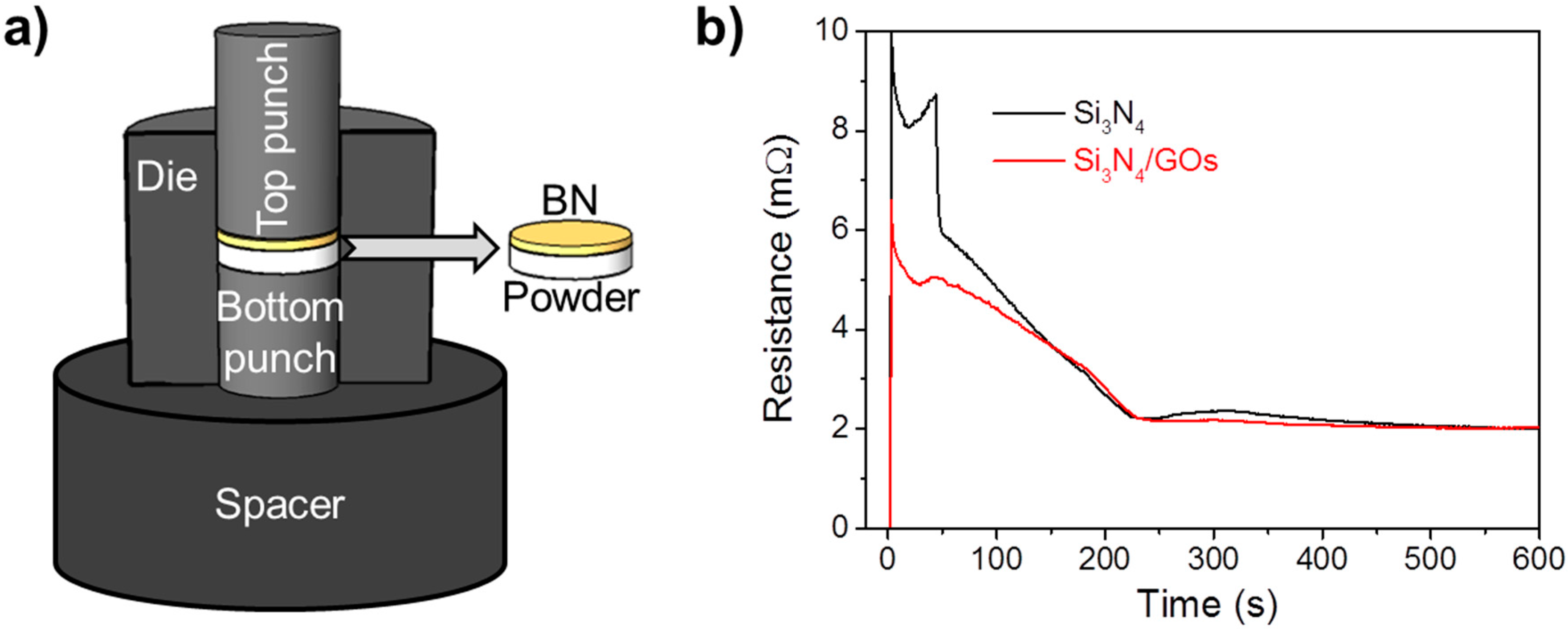
4/GOs composition were introduced into the graphite die and uniaxially pressed at 20 MPa. Next, the punches set-up was modified to achieve an asymmetric configuration (
Figure 1a). In this way, the bottom punch was fully enclosed into the die and leaned on the spacer (Ø = 50 mm); whereas the top punch (Ø = 20 mm) was partially introduced into the die, looking for promoting a different effective current intensity per unit area through the system. A BN slab (thickness = 1 mm) was placed between the composite powder and the top punch. The SPS (SPS-510CE; Fuji Electronic Industrial Co., Ltd., Saitama, Japan) tests were carried out in a vacuum atmosphere of 6 Pa, at a maximum temperature of 1650 °C hold during 5 min, a heating rate of about 133 °C·min
−1 up to 1400 °C and, then, 50 °C·min
−1 from this temperature up to 1650 °C to avoid temperature overshooting, and applying a uniaxial pressure of 50 MPa. The electrical resistance (R) during the SPS run was assessed from the current (I) and voltage (V) data provided online by the equipment.
The density of the sintered specimen was measured in water by the Archimedes’ method once the graphite foil attached to the surface—employed to assure good electrical contact between the powder and punches—was removed. The final dimensions of the ground specimens were ~20 mm in diameter and ~3.2 mm in thickness. The microstructural characterization of the composite was performed by X-ray diffraction (XRD, Bruker D5000, Siemens, Munich, Germany), confocal Raman microscopy (Alpha 3000, WITec GmbH, Erfurt, Germany) and field emission scanning electron microscopy (FESEM, S-4700, Hitachi, Barcelona, Spain). The α/β-Si
3N
4 phase ratio was estimated using the XRD data and the Gazzara and Messier’s method [
14]. In the case of the Raman spectroscopy, a laser wavelength of 532 nm and 2 mW of power were employed, scanning areas of 15 µm width and 4 µm height -taken at the top and bottom of the FGM cross-section-, and using an acquisition of 150 × 40 pixels and an integration time of 0.3 s. FESEM images were obtained on polished and plasma etched surfaces (CF
4/O
2 for 24 s), as well as on fracture surfaces. The mean Si
3N
4 grain diameter (d
50) and aspect ratio (AR
50) were calculated by image analysis methods on FESEM micrographs considering at least 1000 features.
The elastic modulus (E) and hardness (H) were estimated on the FGM cross-section by Vickers indentation applying loads of 98 N (Zhu 2.5, Zwick/Roell, Barcelona, Spain). The fracture toughness (KIC) was determined by both the indentation fracture (IF), using loads of 98 N, and the surface crack in flexure (SCF) methods. In the latter case, tests were carried out according to the ASTM standard C1421-01b by performing a Knoop indentation at 98 N at the center of the top or bottom surfaces of 14.5 × 3.2 × 1.8 mm bars in which the rGOs ab plane is perpendicular to the crack propagation path. The damaged zone after the indentation was gently removed to eliminate residual stresses. Afterwards, the polished bars were 3-point bended with a span of 10 mm and a displacement rate of 0.5 mm·min−1. Similar SCF tests were done in the monolithic FGM for comparison purposes. Data for all mechanical tests correspond to the average value of at least three well-defined measurements. The fracture surfaces were carefully observed by optical microscopy to measure the initial pre-crack size. Finally, the electrical conductivity (σe) of the FGM was assessed by the four-probe DC method (potentiostat/galvanostat, Autolab PGSTAT302N).
3. Results and Discussion
The first evidence of the distinct sintering response of the Si
3N
4/GOs composition as compared to the monolithic ceramics one was the lower voltage attained during the first 150 s (
Figure 1b), i.e., before the pyrometer starts monitoring the temperature. That means that the initial electrical resistance in the SPS system was inferior (~40%) for Si
3N
4/GOs than for Si
3N
4 (
Figure 1b). This fact can be explained because the graphene composite is expected to be more electrical conductor than the monolithic ceramics. Once the pyrometer perfectly followed the programed temperature, the electrical parameters of the SPS were similar, independently of the powders composition.
The whole material exhibited a full densification (~99.5% of the theoretical density) and, in order to elucidate if there is a gradient in the microstructure of the composite, the α-Si
3N
4 phase content along the cross-section of the specimen was first analyzed.
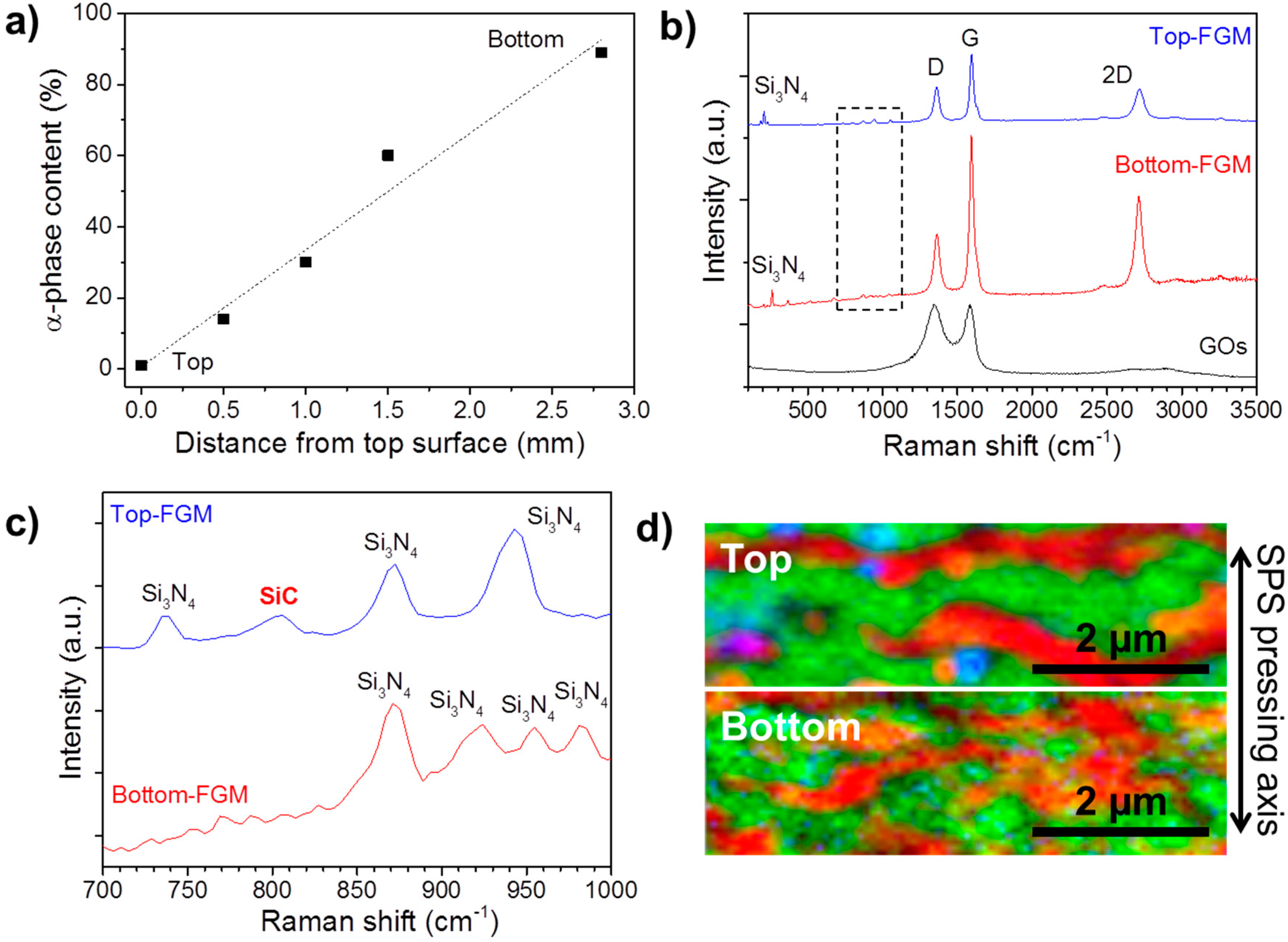
Figure 2a shows a continuous and almost linear reduction of the α-phase content from the bottom surface (89%) towards the top one (1%), where the ceramic matrix was almost fully transformed to β-phase, indicating a gradual α→β-phase transformation across the material thickness. This fact should be associated with the temperature gradient generated during the SPS process due to the special assembly of the punches/BN slab/powder compact, as it will be explained below.
The micro-Raman characterization pointed that GOs were highly in situ reduced (rGOs) during the SPS treatment of the composite (
Figure 2b) in consonance with previous results for Si
3N
4/GOs composites [
13]. This is supported by a strong decrease in the intensity ratio between the D- and G-bands (I
D/I
G), commonly employed as a tool to estimate the defective degree of carbon nanostructures [
15], after the sintering process, as well as by the presence of a well-defined second order of the D-band (2D-band at ~2717 cm
−1). In this way, I
D/I
G diminished from 1.9 in the pristine GOs to ~0.4 in the FGM, highlighting less defectivity of the rGOs into the sintered composite. The extremely high intensity of rGOs bands made complicate to observe the low intense peaks associated to the Si
3N
4 matrix in the range of 150–300 cm
−1 (
Figure 2b) [
16,
17]. Furthermore, few almost undetectable peaks in the 700–1000 cm
−1 region were also distinguished (dashed square in
Figure 2b, enlarged in
Figure 2c). Most of them corresponded to Si
3N
4 [
16,
17], although the transverse optical band of SiC (TO ~795 cm
−1) was also identified at the top surface (
Figure 2c). Taking into account Raman data, false colored images at both sides of the specimen were created (
Figure 2d) by merging the most intense peaks for rGOs (G-band in red color), SiC (TO in blue color) and the region between 175–250 cm
−1 that relates to Si
3N
4 (in green color). As it can be seen, rGO sheets appeared mostly oriented with their basal planes perpendicular to the SPS pressing axis (an effect of the applied pressure). Some blue features, associated to SiC particles, were observed at the top surface, which would be explained by the reaction between the free Si contained into the Si
3N
4 powders and the carbon coming from GOs due to the high temperatures attained in the SPS process [
15] at this location. In view of the low intensity of the SiC Raman band and the lack of XRD signature for this compound, it can be assumed that the SiC content into the FGM is almost negligible.
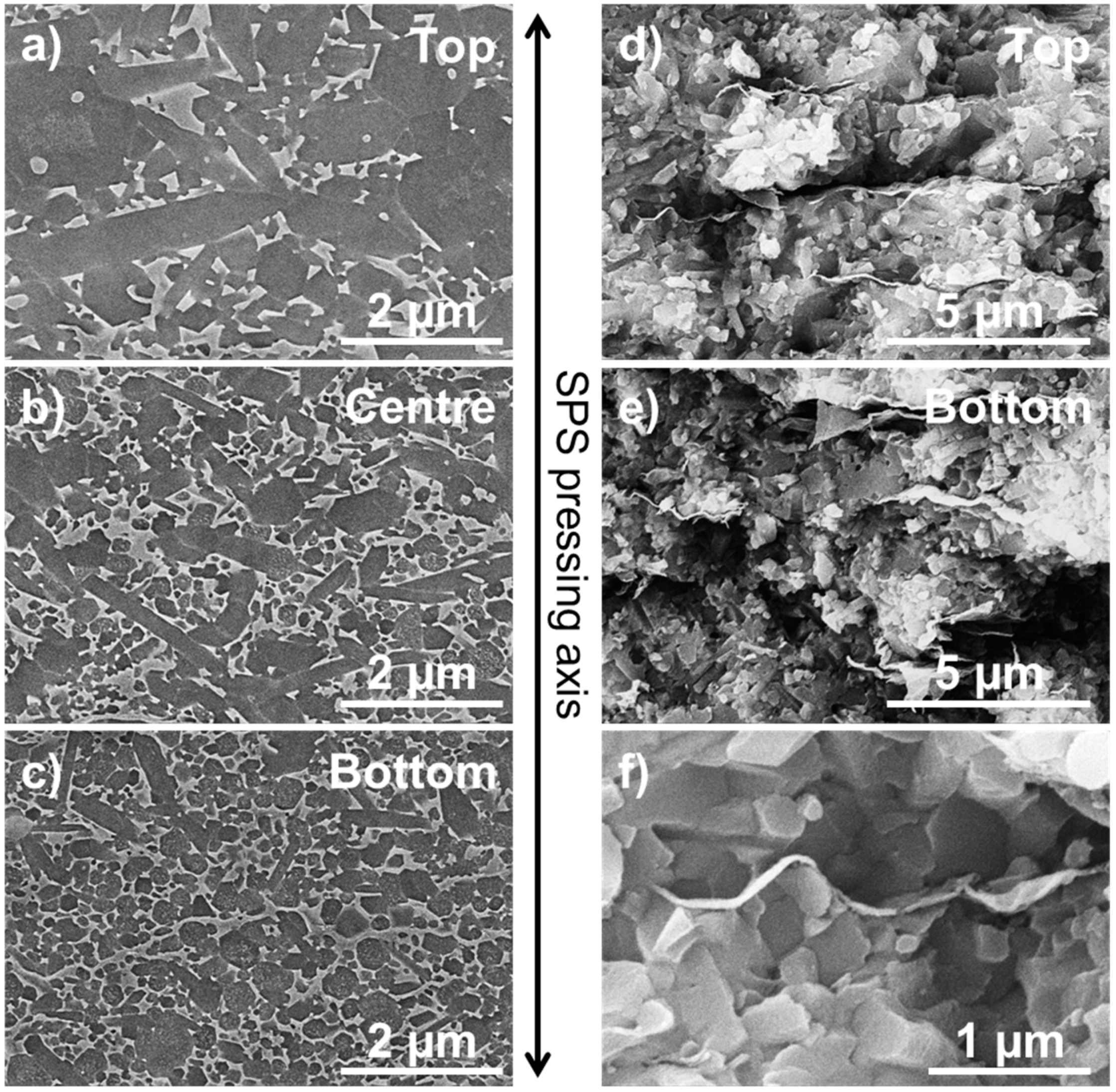
The microstructural analysis performed by FESEM evidenced a progressive growth of the Si
3N
4 grain size (
Figure 3a–c) from the bottom surface of the specimen (d
50 = 230 nm) towards the top surface (d
50 = 570 nm), which corresponded to an augment of ~150%. In addition, grains also evolved to a more elongated shape, increasing AR
50 from 1.6 (bottom) to 1.9 (top), being in good agreement with the larger β-phase content at the top surface. This graded microstructure would be directly linked to temperature differences into the powder compact during the SPS process. In this way, the temperature mismatch between the bottom and top surfaces of a monolithic Si
3N
4 FGM, using the same SPS setting conditions than in the present work, was previously estimated to be around 150 °C [
6]. As the phase transformation gradients in that FGM and in the current Si
3N
4/rGOs FGM are quite similar, a similar temperature difference could be assumed for the rGOs-based FGM. However, the increment in the grain size in the composite FGM was smaller (150%) than in the monolithic Si
3N
4 FGM (240%), which could be explained by the presence of rGOs that would limit the matrix grain growth in the composite [
13]. The fracture surface views of the cross-section of the FGM at the top (
Figure 3d) and at the bottom (
Figure 3e) showed the clear alignment of the rGOs perpendicularly oriented with respect to the SPS pressing axis. A homogeneous dispersion of the rGOs into the matrix was also observed, with the rGO sheets following the ceramic boundaries with a wavy shape (
Figure 3f).
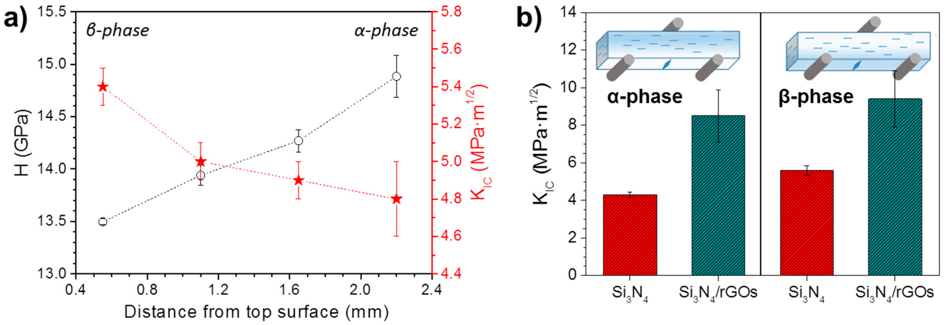
Considering that the Si
3N
4/rGOs specimen exhibits a graded microstructure in terms of matrix grain size and crystalline phase contents, the development of a gradient in the mechanical properties would also be expected. In this sense, the hardness across the composite FGM linearly increased (
Figure 4a) from the top β-phase rich surface (H = 13.5 GPa) to the bottom α-phase rich one (H = 14.9 GPa) in about 10%, with an average rate of 0.9 GPa·mm
−1. This rate is slightly smaller than that reported for the monolithic Si
3N
4 FGM (1.2 GPa·mm
−1), which would be mainly explained by the softening effect played by the graphene-based nanostructures in the hardness of Si
3N
4/graphene composites, attributed to certain sliding of rGOs at the grain boundaries under shear and effects of the rGOs waviness as well [
18]. The analysis of the fracture toughness was initially carried out by IF, although it is not the most appropriate method as median and radial cracks usually are not properly developed in ceramic/graphene composites [
18], but it helps to explain crack path/graphene interactions. In the present case, the maximum load able to generate measurable cracks was 98 N. As it can be seen in
Figure 4a, K
IC displayed values from 4.8 MPa·m
1/2 (bottom surface) to 5.4 MPa·m
1/2 (top surface), which are very similar. Moreover, it would indicate that the reinforcing effect of the rGOs is not really perceived for small cracks and the slight K
IC differences would be attributed to the change in the matrix grain size, as it happens in the monolithic Si
3N
4 FGM. K
IC data by the SCF method were achieved at both sides of the sample for a better estimation of the long-crack toughness of this composite (see scheme of
Figure 4b). In this way, K
IC augmented from 8.2 MPa·m
1/2 (bottom) to 9.4 MPa·m
1/2 (top), which represents an increment of about 15%. Present results suggest that long-crack K
IC values are comparable independently of the surface crack location (top/bottom), probably because composite toughness increases as crack propagates with a R-curve behavior, as measured for other ceramic/graphene composites [
19] and, hence, similar toughness level is reached as cracks propagation progress across the specimen. This mechanical response also indicates that rGOs are determinant in the reinforcing effect of this composite; whereas the degree of phase transformation and development of elongated Si
3N
4 grains would influence the short-crack toughness. K
IC values obtained by SCF are much higher than those attained for monolithic Si
3N
4 FGMs (4.3 MPa·m
1/2 at the bottom and 5.6 MPa·m
1/2 at the top,
Figure 4b) with a grain size gradient similar to the present case, evidencing the large reinforcement capability of rGOs to promote the occurrence of crack shielding mechanisms, such as crack bridging, deflection and branching (see some examples in
Figure 5). Actually, the highest K
IC values for present FGM composite are quite similar to those displayed by an uniform Si
3N
4/rGOs composite of the same composition (K
IC = 10.4 MPa·m
1/2) [
18], thus, pointing to alike reinforcing mechanisms promoted by rGOs, independently of the matrix grain size.
Finally, the electrical conductivity of the Si
3N
4/rGOs FGM reached a value of 64 S·m
−1, about 14 orders of magnitude higher than that for the monolithic Si
3N
4 FGM (~10
−13 S·m
−1), being in the same range than the conductivity reported for Si
3N
4 composites containing 4.3 vol.% of rGOs (97 S·m
−1 [
13]). Despite the insulating nature of Si
3N
4, low additions of GOs are able to create a conducting network within the ceramic matrix extraordinarily increasing the electrical conductivity of the composite. This electrical response would allow, among others, dissipating static charges at the surface FGM specimen or promote the electrical discharge machining of complex Si
3N
4 parts (micro-rotor, micro-turbines, implants) [
20].


