Article

Aerosol Jet Printing and Interconnection Technologies on Additive Manufactured Substrates

1
Institute for Micro Integration (IFM), University of Stuttgart, Allmandring 9b, 70569 Stuttgart, Germany
2
Hahn-Schickard, Allmandring 9b, 70569 Stuttgart, Germany
*
Author to whom correspondence should be addressed.
J. Manuf. Mater. Process. 2022, 6(5), 119; https://doi.org/10.3390/jmmp6050119
Submission received: 29 July 2022 / Revised: 6 September 2022 / Accepted: 20 September 2022 / Published: 9 October 2022

Abstract

:
Nowadays, digital printing technologies such as inkjet and aerosol jet printing are gaining more importance since they have proven to be suitable for the assembly of complex microsystems. This also applies to medical technology applications like hearing aids where patient-specific solutions are required. However, assembly is more challenging than with conventional printed circuit boards in terms of material compatibility between substrate, interconnect material and printed ink. This paper describes how aerosol jet printing of nano metal inks and subsequent assembly processes are utilized to connect electrical components on 3D substrates fabricated by Digital Light Processing (DLP). Conventional assembly technologies such as soldering and conductive adhesive bonding were investigated and characterized. For this purpose, curing methods and substrate pretreatments for different inks were optimized. Furthermore, the usage of electroless plating on printed metal tracks for improved solderability was investigated. Finally, a 3D ear mold substrate was used to build up a technology demonstrator by means of conductive adhesives.

1. Introduction

Digital printing technologies such as inkjet and aerosol jet printing have proven to be suitable for the assembly of complex microsystems [1,2,3,4,5,6,7,8]. The printing results are dependent on many different factors including pre- and post-processing like plasma treatment, laser irradiation [3], as well as drying and curing procedures [5]. Furthermore, the material compatibility between ink and substrate must be taken into consideration [5,9,10,11,12]. In many applications, substrates functionalized by digital printing need to be interconnected to conventionally manufactured parts, such as batteries, sensors, microcontroller units or other electronic components. These so called hybrid printed electronics combine the advantages of printed and conventional electronics [13,14,15]. It is assumed by industry and research that hybrid electronics will play an important role in the future of printed electronics [16]. In order to connect the printed structures with other components, several methods such as soldering, conductive adhesive bonding or overprinting can be applied. In this area, the material interaction and compatibility, e.g., between solder paste or conductive adhesive, respectively, and printed ink, play a decisive role as well [5,11,13,17]. Much work has been carried out regarding the functionalization of injection-molded thermoplastic substrates [1,2,5] and paper-based circuit boards [18,19] by digital printing. Isotropic conductive adhesives (ICA) [13] and low melting solder like bismuth-based solder paste [20] showed promising results. However, as additive manufacturing methods such as Fused Filament Fabrication (FFF), Multi Jet Modelling (MJM) or Digital Light Processing (DLP) are gaining increasing importance, also the materials used in those technologies appear in the focus of interest of digital printing, as well as the desire to print directly onto the 3D objects [6,21,22,23,24].
In this work, it is described how aerosol jet printing of nano metal inks and subsequent packaging processes are utilized for assembly of Surface Mounted Devices (SMD) such as, e.g., a commercial pressure sensor package on the printed structures of ear mold substrates which were additively fabricated by DLP. A novel application of such functionalized ear molds is an in-ear blood-pressure sensor system [25,26]. Special attention is given to widespread interconnect and assembly technologies such as soldering and conductive adhesive bonding. While the solderability is limited due to diffusion processes [27,28] between the metal inks and tin-based solder materials [29,30], the challenge of bonding by isotropic conductive adhesives (ICA) is to realize small structure sizes on 3D substrates by dispensing of the ICA since screen printing is not possible on 3D surfaces. The use of the described technologies enables a digital process chain for the fabrication of novel mechatronic integrated devices.

2. Materials and Methods

Substrate materials. For additive manufacturing of 2D test substrates and 3D ear mold substrates, FotoTec DLP.A (Dreve, Unna, Germany) and Luxaprint 3D mold (DETAX, Ettlingen, Germany) were used. Both materials are UV-curable resins suitable for DLP. Furthermore, also test substrates made from the DLP-capable resin PlastCure Rigid10500 were fabricated. The additive manufacturing was done by digital light processing (ProMaker, Prodways, Montigny-le-Bretonneux, France). This material is suitable for rapid tooling and electronic housings, among other applications.
Printing and sintering equipment. Aerosol jet printing was performed with an Aerosol Jet M3D® deposition system (Optomec, Albuquerque, NM, USA). Pneumatic atomization was used to obtain aerosols from the inks, which were additively deposited with a 150 µm nozzle on the substrates. Photonic curing (UV-VIS provided by a pulsed Xenon lamp) was performed by means of a Pulse Forge 1200 (NovaCentrix, Austin, TX, USA).
Plasma treatment of the substrates was performed to modify the surface characteristics of the substrates using a low-pressure oxygen plasma system PlasmaPrep2 (Gala Instruments, Bad Schwalbach, Germany) and an atmospheric plasma system FG5001 equipped with a rotation nozzle RD1004 (Plasmatreat, Steinhagen, Germany). The treatment time with the low-pressure oxygen plasma system was 4s at a power of 40 W. Parameters for the atmospheric plasma were voltage of 260 V, plasma cycle time of 100%, frequency of 21 kHz and compressed air as working gas. The speed of the substrate table was 100 mm/s.
Inks. The following silver and copper nano metal inks were used for the printing and sintering experiments: Sicrys I30 EG-1 (30 wt% Ag) and Sicrys IC25 EG-1 (25 wt% Cu), both from PV Nanocell; Isr, S-CS01130 (25 wt% Ag, Genes’Ink, Rousset, France); and LAB 2271 (25 wt% Ag, GSB Wahl, Aichwald, Germany).
Electroless plating. The electrolyte ENPLATE LDS CU 400 SC (MacDermid Enthone, Waterbury, CT, USA) was used for copper deposition on the printed structures. Durni-Coat 520-20 (RIAG Oberflächentechnik, CH, Wängi, Switzerland) was used for nickel plating and Aurol 20 (Blendl GmbH, Metzingen, Germany) for the gold finish. The layer thickness was measured by X-ray fluorescence analysis (FISCHERSCOPE X-RAY XDV-SDD, Ger, Helmut Fischer, Windsor, CT, USA).
Test layouts and electrical components. Several test layouts were used for the different experiments. In Figure 1, typical test layouts are shown. The layouts include pads for the assembly of the MEMS-based pressure sensor package (BMP388 with 10 pin land grid array (LGA) and metal lid, top right) and 0603 SMD components in imperial size (bottom, right), as well as conductive tracks for electrical resistance measurements (left).
Solder materials and processes. All solder materials used are listed in Table 1. The low temperature stability of the 3D printed ear mold materials limited the use of standard SAC (SnAgCu) solder. Consequently, mainly low-melting solders based on SnBi were investigated.
The solder paste by Nordson, S42D500A5-A, is composed of 42 wt% tin and 58 wt% bismuth with a solidus temperature of 138 °C. DP5600 by Interflux is composed of 42 wt% tin, 57 wt% bismuth and additionally contains 1 wt% silver in order to achieve a certain “presaturation”. Therefore, the diffusion rate in the interface between silver ink and solder material is reduced. All solder materials were applied in paste form by dispensing with respect to the non-planar target applications using a manual nano-dispense station (Martin-SMT, Germering, Germany) and a precision placement tool (Finetech, Berlin, Germany). The soldering tests were performed in a reflow soldering system Type XXS (N2) (SMT Maschinen- und Vertriebs GmbH & Co. KG, Wertheim, Germany). Different soldering profiles inspired by tolerances according to JEDEC standard (IPC/JEDEC J-STD-020) were tested for the SnBi and SnBiAg solders for different peak temperatures between 155 °C and 180 °C as presented in Figure 2.
Isotropic Conductive Adhesives (ICA). Compared to the established soldering technology, the use of ICA is still limited, especially considering the contact resistance to non-noble metal surfaces. Over time, the contact resistance can increase due to oxidation and galvanic corrosion. Initial reliability tests on printed conductive tracks have yielded promising results for the non-noble metal surfaces as well [31]. In this work, both ICA types specified for noble and non-noble metal surfaces were used (Table 2).
ICA 1 is a two component silver-filled, epoxy-based adhesive for noble surfaces like Au, Ag and AgPd terminations [32]. Furthermore, another electrically conductive adhesive (ICA 2) for SMD attach for non-noble surfaces like Sn, SnPb, OSP, etc., was investigated. Both adhesives were applied in a cartridge for dispensing or as a film for stamping. The curing temperature was varied between 6 h at 80 °C and 30min at 120 °C in a lab oven UF55 from Memmert GmbH, GER.
Characterization of adhesive bond strength. Shear tests according to standard DIN EN 62137-1-2 [33] were utilized to examine the adhesion strength of the ICA bonded SMD. The shear strength of the connections was measured with a Dage 4000 bond tester from Nordson, Westlake, OH, USA.

3. Results and Discussion

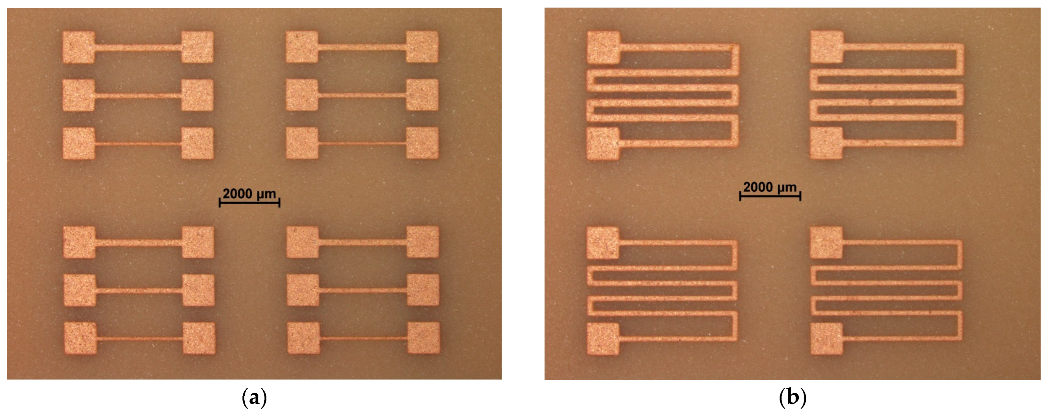
3.1. Printing on 2D Test Substrates

The inks described in Section 2 were evaluated with 2D test substrates made from the materials Luxaprint 3D mold and Fototec DLP A. Thermal sintering at the required temperatures above 140 °C partly led to warpage due to the high substrate thickness of 4 mm and was, therefore, discarded in favor of photonic curing. In Table 3, the results of the complete printing process are shown with respect to printability, photonic curing and adhesion. According to these results, the silver ink Sicrys I30 EG-1 is the most suitable ink for the investigated substrates and printing method.

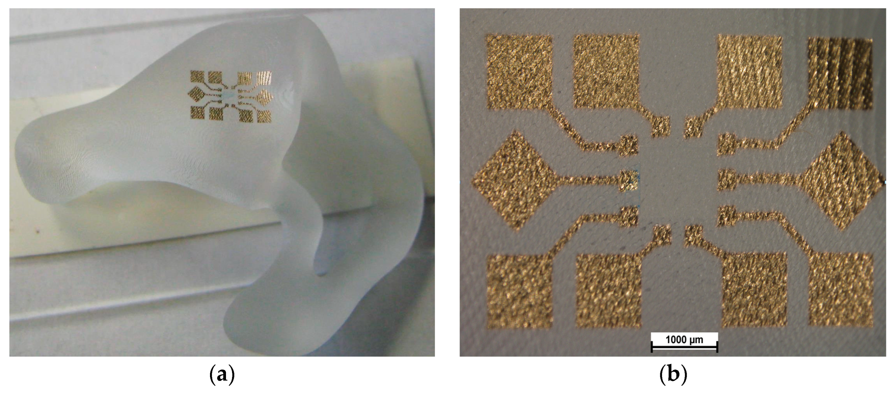
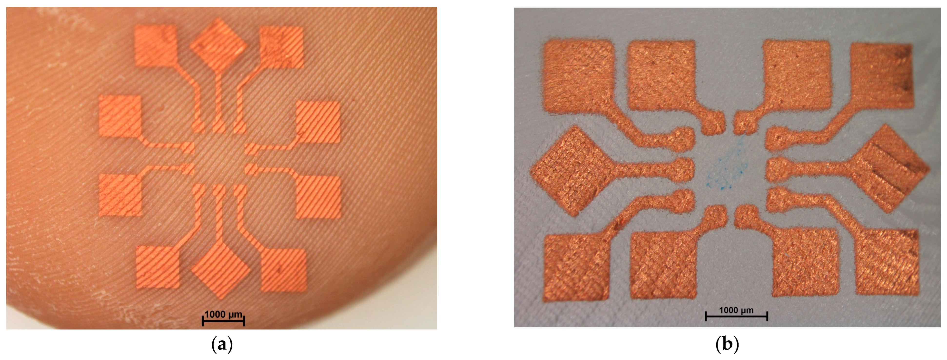
3.2. Printing on 3D Ear Mold Substrates

A further challenge is printing on 3D shaped objects with uneven surfaces and slopes. The aerosol jet system used in these experiments has some 3D capability, as opposed to most inkjet printers which rely on planar substrates. Thus, it was possible to print on certain areas of typical 3D shaped ear mold substrates made from either Fototec DLP A or Luxaprint 3D mold. The printing layout was thereby adapted to the footprint of the used MEMS-based pressure sensor and applied on different 3D substrates based on typical ear molds (Figure 3a and Figure 4a). Conductive structures with high precision and edge sharpness could be printed even on relatively rough surfaces (Figure 3b and Figure 4b).

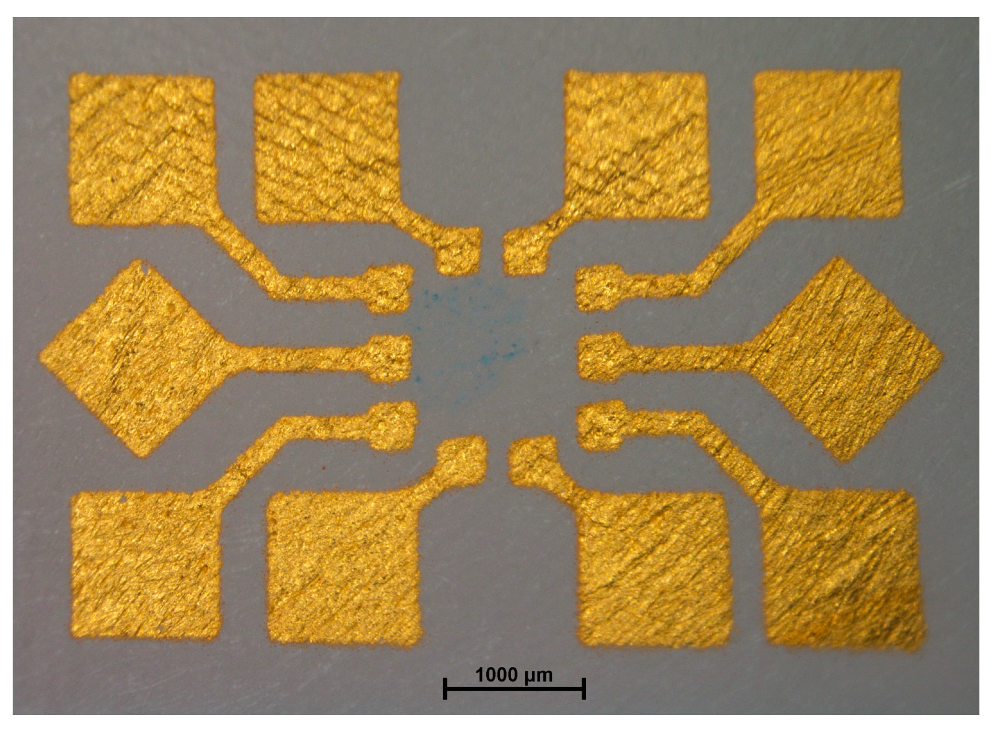
3.3. Electroless Plating on Printed Silver Structures

In order to circumvent the challenge of dissolving the printed tracks in liquid solder due to high diffusion rates of silver described in the previous section, electroless copper plating was used to cover the printed silver tracks. The catalytic behavior of silver [34] makes printed silver a candidate for a starting layer for electroless copper plating. A further advantage of electroless plating is to decrease the electrical resistance and increase the current load capacity of the printed silver tracks. First trials with a plating time of 60 min led to partial delamination of the plated structures (Figure 5a,b), but with a reduction of the plating time to 15 min no such problems occurred (Figure 5c,d). The copper plating was carried out at a process temperature of 48 °C. The copper thickness was approximately 1.4 µm for both substrate materials, which fits to the plating characteristics of the electrolyte. The plating did not visibly affect the Luxaprint 3D material. FotoTec DLP-A, on the other hand, showed a slight deformation. Tape tests after plating for first evaluation of the adhesion were passed for both materials.
By electroless copper plating of test structures on planar test substrates (Figure 6), a significant reduction of the electrical resistance (Table 4) was achieved. Also on 3D substrates, successful electroless copper plating could be carried out (Figure 7). Using Luxaprint 3D mold substrates in combination with the Ag ink Sycris I30 EG-1, on the copper plated patterns a Ni/Au surface finish finally could be applied (Figure 8). Ni/Au plating was carried out using standard plating parameters (plating time of 17 min each at 88 °C (Ni) and 86 °C (Au)).
The differences in electrical resistance between the two materials before the plating process may be due to the different substrate properties, since the printing parameters for both substrates were identical. Chemical and physical material properties of the substrates can influence the wetting behavior of the ink as well as the sintering process. Sintering of conductive inks is influenced by the substrate’s coefficient of thermal expansion, and with regard to photonic sintering by the substrate’s light absorption (e.g., color).

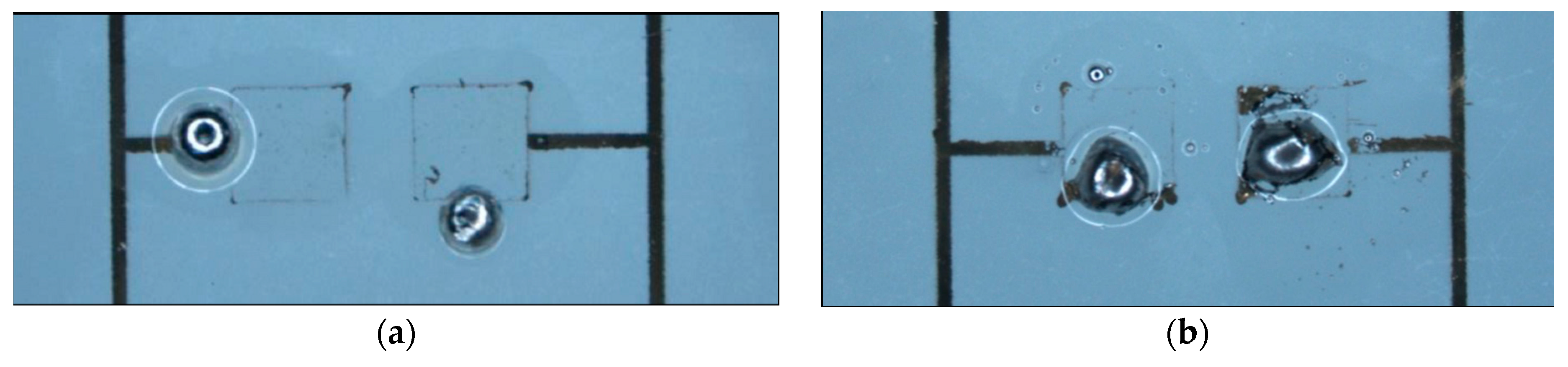
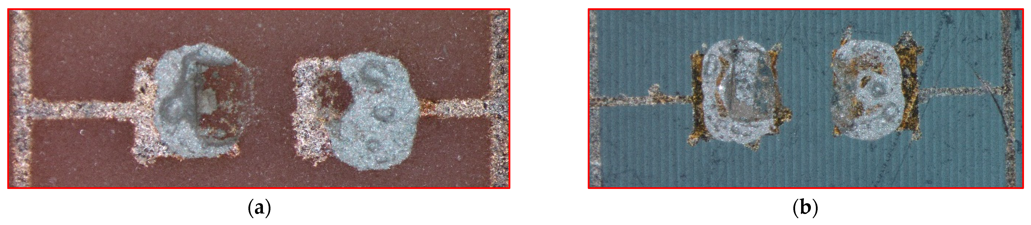
3.4. SMD Assembly on Printed Silver Structures by Soldering

The before mentioned high diffusion rate of Ag in molten solder during soldering leads to a quick leaching of the printed conductor tracks into the solder. Previous works [28] on inkjet-printed conductor tracks showed the influence of the sintering temperature of the inks on the dissolving behavior during the soldering process. In the case of aerosol jet printed thin conductor tracks, the dissolving is even more critical. First, preliminary tests with SAC solder on the 2D test layout confirmed these phenomena on ear mold substrates. The soldering result (5s with hot air) on such printed structures is displayed in Figure 9.
Pads fabricated by aerosol printing of two layers with a thickness of approx. 0.4 µm were dissolved by SnBi solder almost immediately (Figure 10). Residues of the pad’s edges can still be noticed. The results are similar to those obtained on inkjet-printed pads [28,31] where almost all contact pads had conductor breaks after soldering with SnBi solder due to dissolving of the tracks in the soldering paste.
One possible measure to counter the effects of dissolving is to increase the Ag layer thickness by additional printed layers to delay the leaching process. However, this results in longer process times and, thus, in higher production costs. Within this work, up to 12 layers were investigated. To limit the number of layers needed, it is highly desirable to lower the diffusion rate. The rate depends, among other factors, on the process temperature. Thus, by adapting the process parameters the diffusion rate can be lowered. The following parameters had been investigated regarding the influence on the temperature:
  • Reduction of the peak temperature during soldering. A lower temperature leads to a slower diffusion rate. This is also the reason why low melting solders are promising.
  • Increased heating speed and faster cooling for a shorter solder profile and shorter time over liquidus temperature.
Soldering with low-melting SnBi solder on 12 printed Ag layers showed a slightly better behavior. Still, even with increased layer thickness and reduced peak temperature of 155 °C during soldering, the pads were still dissolved as shown in Figure 11. A further reduction of the peak temperature was not feasible because no complete melting of the solder was achieved.
The solder pastes behaved differently depending on the sintering parameters and the inks used for printing the Ag structures, e.g., the meniscus of the solder joint could not be formed on structures made from ink LAB 2271. This concerns especially the wettability that is crucial for an excellent solder connection. The contact angle is far above the limit that could be considered for acceptable wetting (Figure 12). Pretreatment with atmospheric plasma (260 V at a frequency of 21 kHz and traversing speed of 100 mm/s) slightly improved the wetting behavior of the solder on the printed LAB 2271 inks, but was still not satisfying with contact angles over 90°.
Another elementary factor is the material combination of solder and conductive layer, e.g., copper [35,36] dissolves much more slowly in tin than silver [30,37]. The copper inks showed very poor behavior on the used substrate materials, as mentioned before. Based on that, the following other measures regarding the materials were investigated:
  • Using solder with silver content using saturation effects.
  • Electroless copper plating of printed silver layers.
Using solder with silver content leads to a better soldering behavior, so that better solder connections were obtained in the preliminary tests with inkjet-printed Ag pads on 2D substrates [28,31]. On aerosol jet printed structures, the silver content in the solder leads to an improvement as well. Nevertheless, dissolving of the very thin aerosol jet printed layers hinders reproducible soldering results.
Furthermore, in the case of thick-walled substrate bodies, such as ear molds, high thermomechanical forces probably occur during the soldering process, which leads to cracks and consequently damage of the substrates, as can be seen in Figure 13 below. A reflow soldering profile with a lower temperature gradient could reduce thermomechanical stress, but at the same time extend the duration of increased temperature exposure and counterproductively affect the overall diffusion zone.
Unlike the pure Ag printed structures, conductor structures plated with electroless copper could be soldered without any significant dissolving. However, if the process time of electroless copper plating is too long (60 min), the whole structures tend to delaminate partially after soldering, as can be seen in Figure 14a. Nevertheless, if the plating time is only 15 min, the conductor structures consistently withstood the soldering process apart from the cracks in the massive substrate bodies, as shown in Figure 14b. After electroless copper plating of the printed Ag structures, electroless plating of a Ni/Au surface finish also can be carried out. Figure 15 shows pressure sensors soldered onto both ear mold bodies without dissolving the pads. Nevertheless, one can see clearly visible cracks in the substrate due to the effects described above.

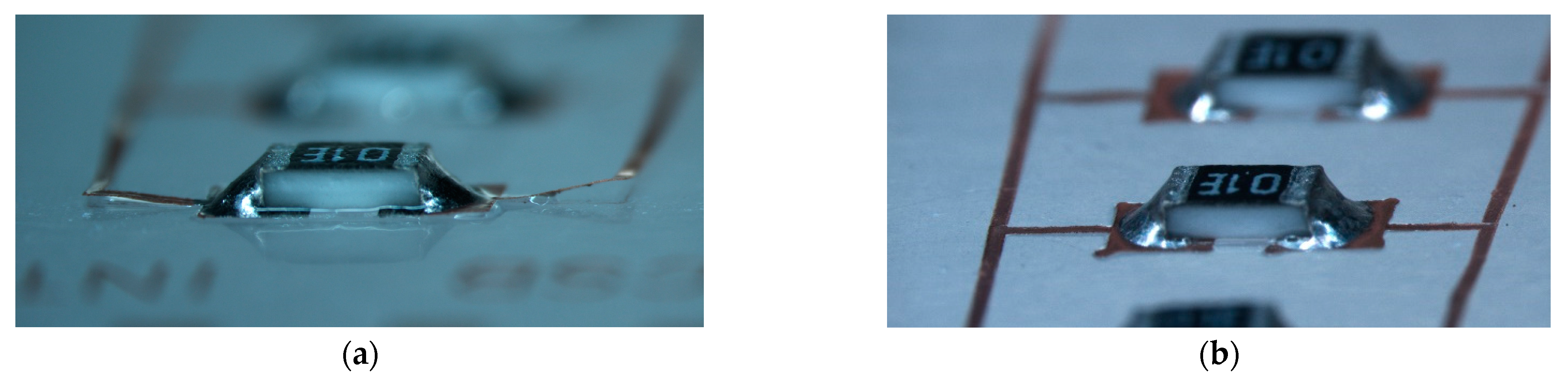
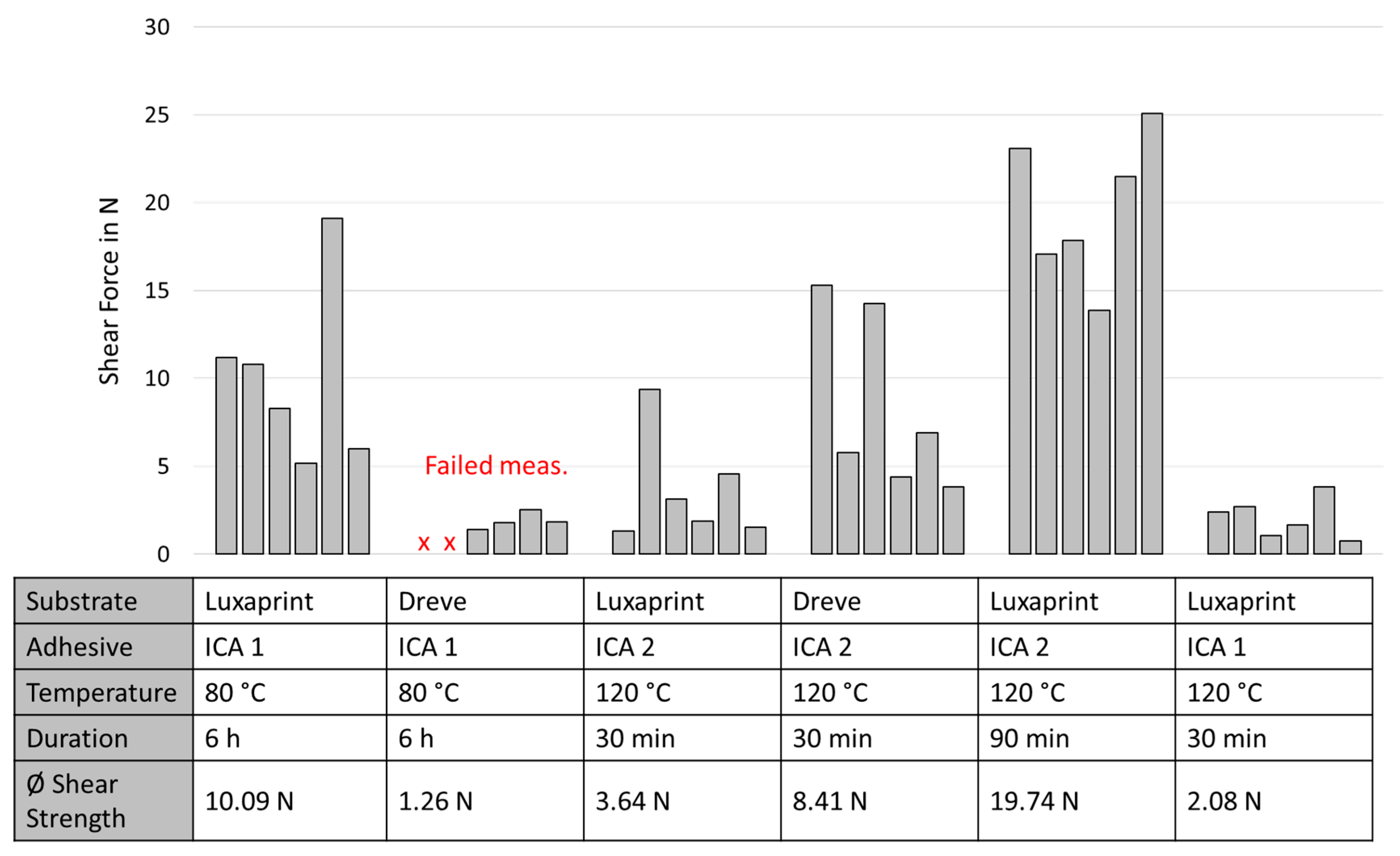
3.5. SMD Assembly on Printed Silver Structures by Means of ICA

Due to the observed cracks in the ear mold material after soldering, adhesive bonding using ICA was investigated. Here, cracks in the substrates do not occur after curing at temperatures around 120 °C and consequently the ear molds withstood all thermal processes for curing the conductive adhesives. Varying the parameters temperature and curing time had a high influence on the adhesion strength. This is reflected by the measured shear strengths of SMD components. The shear strengths of 0603 SMD on the used ear mold materials for both used ICAs and different curing profiles are displayed in Figure 16.
This illustrates that the process parameters have a significant influence on the shear strengths for both substrate materials used. Yet, the fracture patterns are different, as shown in Figure 17. On the substrate made from FotoTec SL.E, the interface between substrate and printed structure partially failed. The overall bond strength on the substrate made from Luxaprint 3D mold is higher. Here, mainly the interface between printed structure and adhesive failed. The reason could be a different roughness and the assumption is that interlocking is the crucial adhesion mechanism.

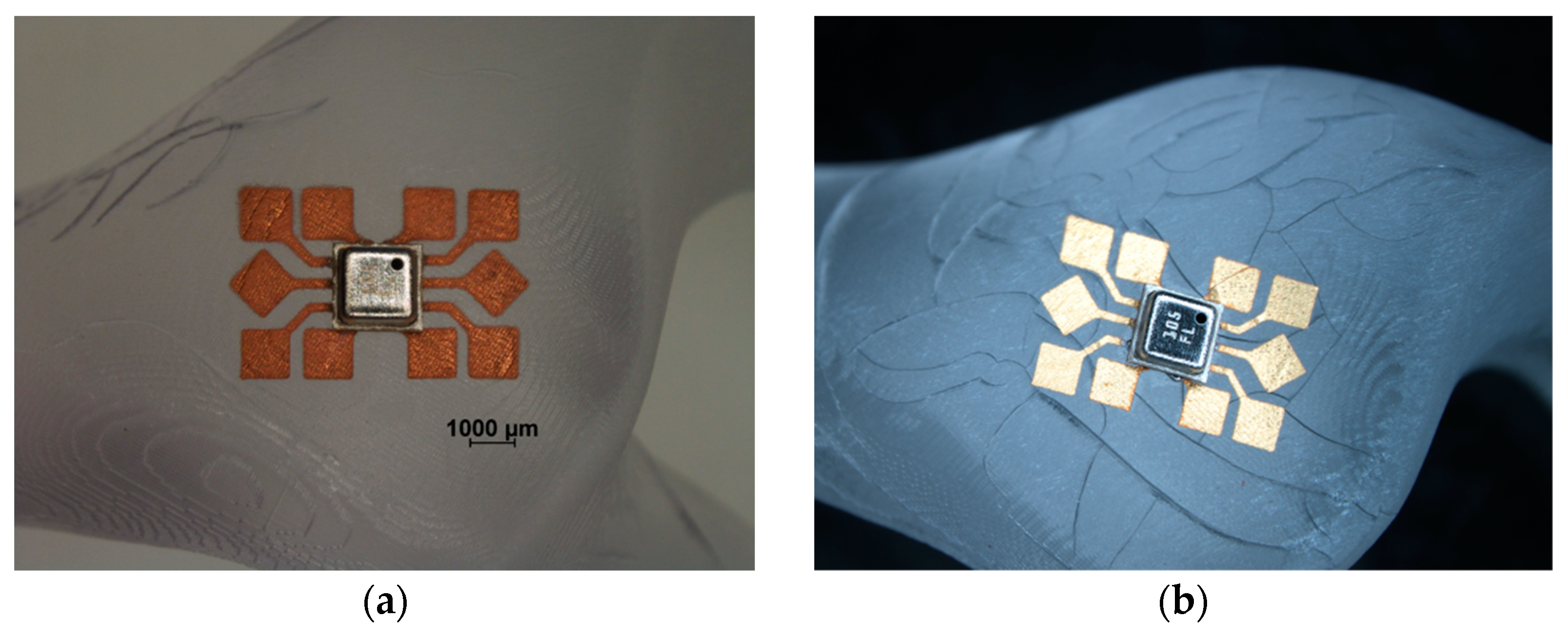
3.6. Functionalized Ear Mold as Technology Demonstrator

For demonstrating the digital process chain using additive manufacturing of the ear mold, aerosol jet printing of the conductor tracks and assembly of the electronic components by ICA, a technology demonstrator (Figure 18) was built up.
The assembly process of electronic components was transferred to a fully automated assembly process on 3D substrates. For automated 3D assembly on production equipment (XTec from Häcker Automation GmbH, Waltershausen, Germany), the ear mold parts are three-dimensionally aligned via a 3D substrate holder with axis system. Position detection is performed by a camera system that can reference the x and y position as well as the z coordinate with high precision. In combination with referencing the components to be assembled from their bottom side after picking, it is possible to assemble with high precision in the same way as on planar substrates. By pin transfer, very small amounts of ICA can be transferred to the 3D substrates, and SMD components with small connection pitches can be assembled. The ICA was cured thermally in a conventional oven. Up to a tilting angle of 45°, no displacement of the assembled components was observed. The SMD components could be successfully electrically contacted on both ear mold materials FotoTec DLP-A and Luxaprint 3D mold, as well as on PlastCure Rigid10500. The latter material was only intended for setting up the assembly process but both, printability and photonic curing, turned out to be very good as well. All demonstrators were realized with five printed Ag layers (ink: Sicrys I30 EG-1) at a tube temperature of 55 °C, sheath gas 70 cm3, atomizer 555 cm³ and impactor 520 cm3.

4. Conclusions

Digital printing enables conductive structures on materials and topographies other than those of printed circuit boards, which opens up a new range of material combinations with customizable properties. Therefore, in this work different DLP-capable substrate materials, nano metal inks and state-of-the-art assembly technologies were selected and investigated. The interconnection technology was conductive adhesive bonding and low-temperature soldering by bismuth-based lead-free solder. The results have demonstrated the challenges but also new possibilities for the combination of those additive manufacturing, digital printing and assembly technologies.
Different nano metal inks (Ag and Cu) were evaluated on substrates made of Luxaprint 3D mold and Fototec DLP A. Thermal sintering at required temperatures above 140 °C led to warpage; therefore, photonic curing was identified as an alternative. The inks showed completely different behavior in terms of printability, photonic curing and adhesion strength. The silver ink Sicrys I30 EG-1 proved to be the most suitable ink for the investigated substrates and printing method. In the end, the results showed that nano metal ink and substrate need to be adapted specifically for each combination.
The possibility to reinforce aerosol jet printed Ag layers on additive manufactured substrates by electroless copper plating with optional Ni/Au surface finish has been shown. This approach did not only reduce the electrical resistance of the layers, but also showed the basic solderability by bismuth-based lead-free solder. However, the substrate materials used showed cracks after the soldering process. Although this leads to the conclusion that this approach is not feasible for both tested UV-curable resin materials, it shows the general potential for other materials and complex geometries. This is especially of interest if reduction of the electrical resistance, increasing current carrying capacity and solderability are desired.
Unlike soldering, ICA has proven to be a viable option for SMD assembly on aerosol jet printed structures on several substrate materials. The achieved shear forces of attached 0603 SMD components strongly depended on the curing profiles. The applicability of ICA by dispensing for SMD assembly on 3D-shaped substrates has been shown.
Combining additive manufacturing, functionalization by aerosol jet printing of nano silver inks and photonic sintering, and conductive adhesive bonding enables a novel digital process chain for functionalized and individualized products from different branches. Further work will focus on the reliability of the advanced functional integration of sensor components, the aforementioned printing and interconnection technologies, and the scalability of the digital process chain. More detailed research is needed to understand the cause–effect relationship between ink and substrate material.

Author Contributions

Conceptualization, K.W.; methodology, K.W. and J.K.; investigation, J.K., K.W. and E.M.; resources K.W., K.G. and M.B.; data curation, E.M.; writing—original draft preparation, K.W. and J.K.; writing—review and editing, M.B., T.H., S.B. and J.J.; visualization, K.W., J.K. and E.M.; supervision, K.W.; funding acquisition, K.G., W.E. and A.Z. All authors have read and agreed to the published version of the manuscript.

Funding

This research was part of the project “Mikroelektronik für permanente, nichtinvasive Blutdruckmessung im Ohr (MikroBo)” funded by the Federal Ministry of Education and Research (BMBF), grant number 16ES0772.

Data Availability Statement

All data used are shown in the text. Raw data are available on request.

Acknowledgments

The authors would like to acknowledge the support of the Bundesministerium für Bildung und Forschung (BMBF) within the research of the funded project “Mikroelektronik für permanente, nichtinvasive Blutdruckmessung im Ohr (MikroBo)”. Further thanks are extended to the project partners of MikroBo.

Conflicts of Interest

The authors declare no conflict of interest.

References

  1. Polzinger, B.; Matic, V.; Liedtke, L.; Keck, J.; Hera, D.; Günther, T.; Eberhardt, W.; Kück, H. Printing of Functional Structures on Molded 3D Devices. Adv. Mater. Res. 2014, 1038, 37–42. [Google Scholar] [CrossRef]
  2. Polzinger, B.; Eberhardt, W.; Ilchmann, A.; Keck, J.; Matic, V.; Kück, H. Drucken von leitfähigen Strukturen Auf spritzgegossenen Thermoplastischen Bauteilen. Prod. Von Leit. Syst. 2012, 14, 1401. [Google Scholar]
  3. Trotter, M.; Juric, D.; Bagherian, Z.; Borst, N.; Gläser, K.; Meissner, T.; von Stetten, F.; Zimmermann, A. Inkjet-Printing of Nanoparticle Gold and Silver Ink on Cyclic Olefin Copolymer for DNA-Sensing Applications. Sensors 2020, 20, 1333. [Google Scholar] [CrossRef] [PubMed] [Green Version]
  4. Matic, V.; Keck, J.; Ilchmann, A.; Polzinger, B.; Eberhardt, W.; Kück, H. Printing of Functional Silver Structures on Polymer Based 3D-Packages. In Proceedings of the 10th International Conference on Multi-Material Micro Manufacture, Vienna, Austria, 9–11 October 2012. [Google Scholar]
  5. Polzinger, B.; Jürgen, K.; Eberhardt, W.; Gläser, K. Inkjet-Printed Metal Lines and Sensors on 2D and 3D Plastic Substrates. In Handbook of Industrial Inkjet Printing: A Full System Approachinkjet-Printed Metal Lines and Sensors on 2D and 3D Plastic Substrates; Vol. Handbook of industrial inkjet printing: A full system approach; Wiley-VCH: Weinheim, Germany, 2018; pp. 617–632. [Google Scholar]
  6. Amend, P.; Goth, C.; Franke, J.; Frick, T.; Schmidt, M. ADDIMID Technology and Aerosol Jet Printing for Functional MID Prototypes by the Use of Stereolithography. In Proceedings of the 10th International Congress Molded Interconnect Devices (MID), Fuerth, Germany, 19–20 September 2012. [Google Scholar]
  7. Hedges, M. 3D Aerosol Jet® Printing-Adding Electronics Functionality to RP/RM. In Proceedings of the DDMC 2012 Conference, Berlin, Germany, 14–15 March 2012; pp. 1–5. [Google Scholar]
  8. Hedges, M. 3D Printed Electronics via Aerosol Jet®-Applications & Manufacturing Technology. In Proceedings of the Presented at the 3D Printing Electronics Conference, Eindhoven, The Netherlands, 26 March 2014. [Google Scholar]
  9. Cummins, G.; Desmulliez, M.P.Y. Inkjet Printing of Conductive Materials: A Review. Circuit World 2012, 38, 193–213. [Google Scholar] [CrossRef]
  10. Yan, K.; Li, J.; Pan, L.; Shi, Y. Inkjet Printing for Flexible and Wearable Electronics. APL Mater. 2020, 8, 120705. [Google Scholar] [CrossRef]
  11. Keck, J. Benefits and Challenges of Digital Printing for Printed Electronics. In Proceedings of the Inkjet Conference 2019, Neuss, Germany, 29–30 October 2019. [Google Scholar]
  12. Nayak, L.; Mohanty, S.; Nayak, S.K.; Ramadoss, A. A Review on Inkjet Printing of Nanoparticle Inks for Flexible Electronics. J. Mater. Chem. C 2019, 7, 8771–8795. [Google Scholar] [CrossRef]
  13. Niittynen, J.; Kiilunen, J.; Putaala, J.; Pekkanen, V.; Mäntysalo, M.; Jantunen, H.; Lupo, D. Reliability of ICA Attachment of SMDs on Inkjet-Printed Substrates. Microelectron. Reliab. 2012, 52, 2709–2715. [Google Scholar] [CrossRef]
  14. Miettinen, J.; Pekkanen, V.; Kaija, K.; Mansikkamäki, P.; Mäntysalo, J.; Mäntysalo, M.; Niittynen, J.; Pekkanen, J.; Saviauk, T.; Rönkkä, R. Inkjet Printed System-in-Package Design and Manufacturing. Microelectron. J. 2008, 39, 1740–1750. [Google Scholar] [CrossRef]
  15. Pekkanen, V.; Mäntysalo, M.; Kaija, K.; Mansikkamäki, P.; Kunnari, E.; Laine, K.; Niittynen, J.; Koskinen, S.; Halonen, E.; Caglar, U. Utilizing Inkjet Printing to Fabricate Electrical Interconnections in a System-in-Package. Microelectron. Eng. 2010, 87, 2382–2390. [Google Scholar] [CrossRef]
  16. Lupo, D.; Kirchmeyer, S.; Hecker, K.; Krausmann, J. OE-A Roadmap for Organic and Printed Electronics, 8th ed.; OE-A (Organic and Printed Electronics Association): Frankfurt, Germany, 2020; ISBN 978-3-8163-0736-5. [Google Scholar]
  17. Jäger, J.; Buschkamp, S.; Werum, K.; Gläser, K.; Grözinger, T.; Eberhardt, W.; Zimmermann, A. Contacting Inkjet-Printed Silver Structures and SMD by ICA and Solder. IEEE Trans. Compon. Packag. Manuf. Technol. 2022, 12, 1232–1240. [Google Scholar] [CrossRef]
  18. Andersson, H.A.; Manuilskiy, A.; Haller, S.; Hummelgård, M.; Sidén, J.; Hummelgård, C.; Olin, H.; Nilsson, H.-E. Assembling Surface Mounted Components on Ink-Jet Printed Double Sided Paper Circuit Board. Nanotechnology 2014, 25, 94002. [Google Scholar] [CrossRef]
  19. Andersson, H.; Siden, J.; Skerved, V.; Li, X.; Gyllner, L. Soldering Surface Mount Components Onto Inkjet Printed Conductors on Paper Substrate Using Industrial Processes. IEEE Trans. Compon. Packag. Manuf. Technol. 2016, 6, 478–485. [Google Scholar] [CrossRef]
  20. Krzeminski, J.; Kanthamneni, A.; Wagner, D.; Detert, M.; Schmidt, B.; Jakubowska, M. Microscale Hybrid Flexible Circuit Printed with Aerosol Jet Technique. IEEE Trans. Nanotechnol. 2018, 17, 979–984. [Google Scholar] [CrossRef]
  21. Espalin, D.; Muse, D.W.; MacDonald, E.; Wicker, R.B. 3D Printing Multifunctionality: Structures with Electronics. Int. J. Adv. Manuf. Technol. 2014, 72, 963–978. [Google Scholar] [CrossRef]
  22. Gausemeier, J.; Echterhoff, N.; Kokoschka, M.; Wall, M. Thinking Ahead the Future of Additive Manufacturing-Innovation Roadmapping of Required Advancements; Heinz Nixdorf Institute, University of Paderborn: Paderborn, Germany, 2011; p. 103. [Google Scholar]
  23. Goth, C.; Putzo, S.; Franke, J. Aerosol Jet Printing on Rapid Prototyping Materials for Fine Pitch Electronic Applications. In Proceedings of the 2011 IEEE 61st Electronic Components and Technology Conference (ECTC), Lake Buena Vista, FL, USA, 31 May 2011–3 June 2011; pp. 1211–1216. [Google Scholar]
  24. Macdonald, E.; Salas, R.; Espalin, D.; Perez, M.; Aguilera, E.; Muse, D.; Wicker, R.B. 3D Printing for the Rapid Prototyping of Structural Electronics. IEEE Access 2014, 2, 234–242. [Google Scholar] [CrossRef]
  25. Werum, K.; Keck, J. Permanent Non-Invasive in-Ear Blood Pressure Measurement. Magazin Inno 2020, 25, 16. [Google Scholar]
  26. Werum, K. Funktionalisierte Otoplastiken Volladditiv Herstellen; Mikroproduktion: Mainburg, Germany, 2021; ISSN 1614-4538. [Google Scholar]
  27. Jiang, Q.; Tu, N.; Lo, J.C.C.; Ricky Lee, S.W. Solderability Analysis of Inkjet-Printed Silver Pads with SAC Solder Joints. In Proceedings of the 2022 International Conference on Electronics Packaging (ICEP), Sapporo, Japan, 11–14 May 2022; pp. 65–66. [Google Scholar]
  28. Juric, D.; Hämmerle, S.; Gläser, K.; Eberhardt, W.; Zimmermann, A. Assembly of Components on Inkjet-Printed Silver Structures by Soldering. IEEE Trans. Compon. Packag. Manuf. Technol. 2019, 9, 156–162. [Google Scholar] [CrossRef]
  29. Hillman, D.; Wilcoxon, R.; Pearson, T.; McKenna, P.; Collins, R. Dissolution Rate of Specific Elements in Sac305 Solder. Proceedings of SMTA International, Rosemont, IL, USA, 14–18 October 2018. [Google Scholar]
  30. Berg, H.; Hall, E.L. Dissolution Rates and Reliability Effects of Au, Ag, Ni and Cu in Lead Base Solders. In Proceedings of the 11th Reliability Physics Symposium, Las Vegas, NV, USA, 3–5 April 1973; pp. 10–20. [Google Scholar]
  31. IGF-Vorhaben-Nr. 20337. N: Kontaktierung Gedruckter Leitfähiger Strukturen (KonsDruckt); Stuttgart, Germany, 2021.
  32. Datasheet EPO-TEK H20E; Epoxy Technology, Inc.: Billerica, MA, USA, 2021.
  33. Deutsche Fassung EN 62137-1-2:2007; Oberflächenmontage-Technik –Verfahren zur Prüfung auf Umgebungseinflüsse und zur Prüfung der Haltbarkeit von Ober-Flächen-Lötverbindungen –Teil 1-2: Scherfestigkeitsprüfung (IEC 62137-1-2:2007). International Standards: Genava, Switzerland, 2007.
  34. Keck, J. Printed Ferrite-Based Toroidal Core Coils as Magnetic Field Sensors. In Proceedings of the Presented at the MST-Kongress 2013, Aachen, Germany, 4–5 June 2013. [Google Scholar]
  35. Snugovsky, L.; Ruggiero, M.A.; Perovic, D.D.; Rutter, J.W. Experiments on Interaction of Liquid Tin with Solid Copper. Mater. Sci. Technol. 2003, 19, 866–874. [Google Scholar] [CrossRef]
  36. Izuta, G.; Tanabe, T.; Suganuma, K. Dissolution of Copper on Sn-Ag-Cu System Lead Free Solder. Solder. Surf. Mt. Technol. 2007, 19, 4–11. [Google Scholar] [CrossRef]
  37. Bulwith, R.A.; Mackay, A. Silver Scavenging Inhibition of Some Silver Loaded Solders. Weld. J. 1985, 7, 86s–90s. [Google Scholar]
Figure 1. Typical test layouts on 2D test substrates (Luxaprint 3D mold, substrate dimension 40 × 40 mm2).
Jmmp 06 00119 g001
Figure 2. Measured temperature profiles for different peak temperatures.
Jmmp 06 00119 g002
Figure 3. Aerosol jet printed Ag structures (ink: Sicrys I30 EG-1) on 3D ear mold substrate (Fototec DLP A) after photonic curing (a). Landing pads for pressure sensor in detail (b).
Jmmp 06 00119 g003
Figure 4. Aerosol jet printed Ag structures (ink: Sicrys I30 EG-1) on 3D ear mold substrate (Luxaprint 3D mold) after photonic curing (a). Landing pads for pressure sensor in detail (b).
Jmmp 06 00119 g004
Figure 5. Electroless copper plating on printed silver tracks (ink: Sicrys I30 EG-1) on 2D test substrates with 60min plating time on Dreve FotoTec DLP-A (a) and on Luxaprint 3D mold (b) and with 15min plating time on Dreve FotoTec DLP-A (c) and on Luxaprint 3D mold (d).
Jmmp 06 00119 g005
Figure 6. Aerosol jet printed Ag structures (ink: Sicrys I30 EG-1) on 2D test substrate after electroless copper plating on Fototec DLP A. Test layout with La, Lb and Lc (a) and Ma and Mb (b) structures (La: 3 mm line, Lb: 3 parallel 3 mm lines with a distance of 30 µm between each other, Lc: 5 parallel 3mm lines with a distance of 30 µm between each other, Ma: 35 mm meander, Mb: 35 mm meander consisting of 3 parallel lines with a distance of 30 µm between each other).
Jmmp 06 00119 g006
Figure 7. Aerosol jet printed Ag structures (ink: Sicrys I30 EG-1) on 3D ear mold substrate after electroless copper plating on Fototec DLP A (a) and Luxaprint 3D mold (b).
Jmmp 06 00119 g007
Figure 8. Aerosol jet printed Ag structures (ink: Sicrys I30 EG-1) on 3D ear mold substrate (Luxaprint 3D mold) after electroless plating with copper, nickel and gold.
Jmmp 06 00119 g008
Figure 9. Hot air soldering with SAC solder on printed Ag structures (ink: Sicrys I30 EG-1) on 2D test substrates (Luxaprint 3D mold) at 255 °C (a) and with SnBi solder at 180 °C (b).
Jmmp 06 00119 g009
Figure 10. Aerosol jet printed Ag structures (ink: Sicrys I30 EG-1) on 2D test substrate (Luxaprint 3D mold) after soldering with SnBi solder in reflow oven with peak temperature of 180 °C.
Jmmp 06 00119 g010
Figure 11. Aerosol jet printed Ag structures with 12 printed layers (ink: Sicrys I30 EG-1) on Luxaprint 3D mold after soldering with SnBi solder in reflow oven with 155 °C peak temperature.
Jmmp 06 00119 g011
Figure 12. Aerosol jet printed Ag structures with LAB 2271 ink after soldering with SnBi solder at 180 °C.
Jmmp 06 00119 g012
Figure 13. Cracks in ear mold substrate after reflow soldering with 180 °C peak temperature (a). Close-in view of crack through conductor path (b).
Jmmp 06 00119 g013
Figure 14. Soldering of 0603 SMD with SnBi solder at 180 °C on aerosol jet printed Ag structures after electroless copper plating (substrate: Luxaprint 3D mold). Plating time 60 min (a) and 15 min (b).
Jmmp 06 00119 g014
Figure 15. Soldering of pressure sensor BMP388 with SnBi solder at 180 °C (substrate: Luxaprint 3D mold). Aerosol jet printed Ag structures after electroless copper plating (15 min) (a). Aerosol jet printed Ag structures after electroless copper plating (15 min) and electroless plating with Ni/Au surface finish (b).
Jmmp 06 00119 g015
Figure 16. Shear forces of 0603 SMD components with different curing profiles.
Jmmp 06 00119 g016
Figure 17. Fracture pattern after shear test. (a) FotoTec SL.E with ICA 2 cured for 30min at 120 °C and (b) Luxaprint 3D mold with ICA 2 cured for 90 min at 120 °C.
Jmmp 06 00119 g017
Figure 18. Technology demonstrator with base body made from three different materials (a). Detail with assembled pressure sensor and 0603 SMD on PlastCure Rigid10500 substrate by means of ICA (b).
Jmmp 06 00119 g018
Table 1. Overview of used solder materials.
Solder TypeAbbreviationCompositionMelting Point
Nordson S42D500A5-ASnBiSn42Bi58138 °C
Interflux DP5600SnBiAgSn42Bi57Ag1139 °C
Table 2. Overview of used ICA.
AdhesiveAbbreviationEpoxy SystemMainly Used Curing Profile
EPO-TEK H20EICA 1Two component system30 min/120 °C
IQ-BOND 5409-CE-X2ICA 2One component system 30 min/120 °C
Table 3. Evaluation results of tested nano metal inks. Adhesion testing was done with a 3M Scotch Tape (rating scale: ++: very good, +: good, O: fair, -: poor, --: very poor).
InkPrintabilityPhotonic CuringAdhesion
Fototec DLP ALuxaprint 3D MoldFototec DLP ALuxaprint 3D Mold
Ag Sicrys I30 EG-1+O/++++++
Cu Sicrys IC25 EG-1+--------
Ag Lab 2271O-++-
Ag S-CS01130O/-++-++
Table 4. Resistance values (Ω) before and after 15 min electroless copper plating on printed silver lines (ink: Sicrys I30 EG-1).
Fototec DLP ALuxaprint 3D Mold
Before PlatingAfter PlatingBefore PlatingAfter Plating
La (n = 8)-0.64 ± 0.3434.73 ± 13.521.06 ± 0.38
Lb (n = 8)158.26 ± 132.470.41 ± 0.0610.08 ± 2.940.63 ± 0.07
Lc (n = 8)34.06 ± 4.170.38 ± 0.075.43 ± 2.840.51 ± 0.19
Ma (n = 4)455.10 ± 227.553.10 ± 1.5884.47 ± 44.534.13 ± 2.07
Mb (n = 4)179.75 ± 107.442.20 ± 0.4249.53 ± 25.563.13 ± 1.57
Publisher’s Note: MDPI stays neutral with regard to jurisdictional claims in published maps and institutional affiliations.

