Abstract
Pull-in effect is a common phenomenon during anodic bonding, a key step in the fabrication processes of capacitive sensors and actuators. To assist the designs and fabrications of these transducers, this paper presents an analytical method for modelling the pull-in effect during anodic bonding. The pull-in effect model was verified by finite element analysis and a verification experiment respectively. The verification results indicate that the analytical method for modelling the pull-in effect during anodic bonding is capable for predicting pull-in voltages of anodically bonded capacitive sensors and actuators in a universal and practical manner without any additional fabrication process.
1. Introduction
If a deformable electrode is forced by an electrostatic voltage beyond the upper limit which is balanced by the mechanical restoring force, it will come into contact with a fixed feature and remain attached after the electrostatic voltage switched off (see Figure 1). This is the so-called pull-in effect and the critical voltage is called pull-in voltage [1]. For anodically bonded capacitive sensors and actuators, due to small gaps and large areas of capacitor plates with deformable features and extremely high bonding voltages, the pull-in effect frequently occurs during anodic bonding, and is unacceptable under most conditions [2,3,4], while useful in some specific applications [5]. To avoid or utilize the pull-in effect during anodic bonding, existing approaches consist of adding additional processes to microfabrication flows [2], the numerical method [3] and the finite element analysis [4]. This paper presents an analytical method for modeling the pull-in effect during anodic bonding in a universal and practical manner without any additional fabrication process.
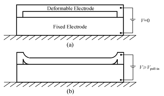
Figure 1.
Pull-in effect. (a) Initial structure without voltage bias and (b) attached structure with a voltage bias beyond pull-in voltage.
2. Methods
During anodic bonding, the deformable electrode of the silicon wafer deforms under an electrostatic force Fe generated by a bonding voltage and maintains a stable state with the contribution of a mechanical restoring force Fm (see Figure 2). As the wafer deforms further under an increasing voltage, the applied forces increase and remain stable until reaching the critical stable state when the pull-in effect occurs (see Figure 3). At the critical stable point, the electrostatic force and the mechanical restoring force are equal and simultaneously the two curve gradients of the two forces are also identical. Therefore, the only solution for the displacement when the pull-in effect occurs is xpull-in = d/3, and the pull-in voltage is
where km is the equivalent mechanical elastic coefficient, d is the distance between the deformable and fixed electrodes, i.e., the cavity depth of the capacitor formed by anodically bonding the etched silicon wafer and the glass wafer, ε0 is the permittivity of vacuum and A is the overlapping area of the two electrodes.
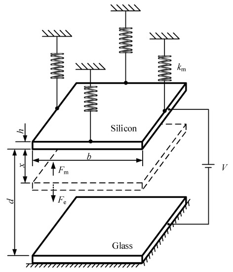
Figure 2.
Force analysis of the silicon diagram during anodic bonding.
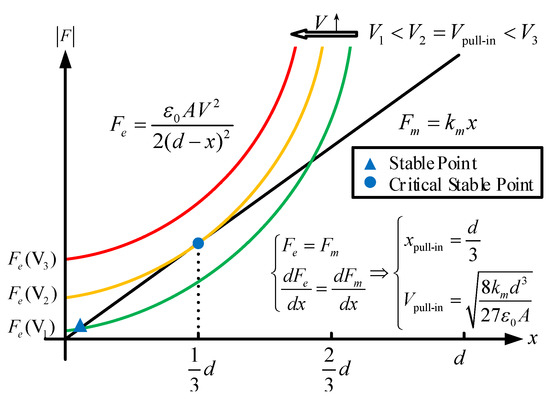
Figure 3.
Derivation for the pull-in voltage.
For rectangular or circular diagrams commonly used in MEMS applications, the equivalent mechanical elastic coefficient is expressed as
where E, h, α and b are the Young’s modulus, the thickness, the shape factor and the feature length of the diaphragm respectively. As shown in Table 1, for a rectangular diagram, the shape factor is determined by the ratio of the long edge length a to the short edge length b set as the feature length; for a circular diagram, the diameter is set as the feature length. Consequently, the pull-in voltage is found to be

Table 1.
Shape factors of rectangular and circular diagrams.
3. Results and Discussion
To verify the method for modelling the pull-in effect, a finite element analysis and a verification experiment were both performed to compare with calculated pull-in voltages. In the term of the finite element analysis, nine sets of parameters selected according to orthogonal design were simulated and the relative deviations between simulated values and calculated values are 0.5~7.7%, with an average relative deviation of 4.5% (see Figure 4).
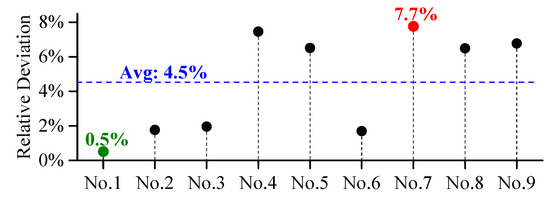
Figure 4.
Relative deviations between simulated values and calculated values.
In the term of the verification experiment, to balance the effectiveness and the number of the verification experiment, seven pairs of etched silicon wafers and bare glass wafers were anodically bonded with bonding voltages of 800 V. Before that, the silicon wafers with four different thicknesses were etched for four different etching depths according to the patterns shown in Figure 5. The deviations between calculated pull-in voltages and experimental results are shown in Figure 6 and the ratio of grade deviation 0, i.e., the accuracy of predicting the pull-in effect is 87%. The ratios of grade deviation −1 and −2 are respectively higher than those of grade deviation 1 and 2, which indicate that the calculated pull-in voltages are approximately higher the actual pull-in voltages, partly due to the influence of high bonding temperature on the Young’s modulus. Besides, the deviations are also related to differences in thicknesses of silicon wafers, manufacturing errors of etching depths and widths, etc. The results of the finite element analysis and the verification experiment validate the effectiveness of the analytical method for modelling the pull-in effect during anodic bonding.
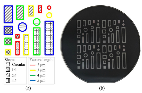
Figure 5.
Verification experiment on the pull-in effect. (a) Design of etching patterns on silicon wafers and (b) an example image (d: 2 μm, h: 400 μm) of the seven pull-in effect results. The patterns with dark fillings indicate the occurrences of the pull-in effect.
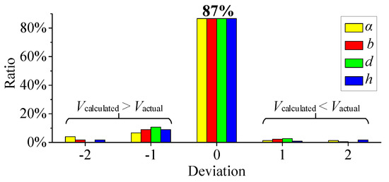
Figure 6.
Comparison between calculated pull-in voltages and experimental results.
4. Conclusions
A pull-in effect model during anodic bonding for analytically calculating pull-in voltage has been built and verified. The verification results of the finite element analysis and the verification experiment validate the effectiveness of the pull-in effect model, exhibit the capability of predicting pull-in voltages in a universal and practical manner, and indicate the feasibility of optimizing designs and fabrications for anodically bonded capacitive sensors and actuators.
Author Contributions
Q.W., D.C. and J.W. conceived and designed the experiments; Q.W. and B.X. performed the experiments; Y.L. contributed analysis tools; Q.W. and J.C. wrote the paper.
Acknowledgments
This work was supported by the National Key R&D Program of China under Grant 2018YFF01010400 and the National Natural Science Foundation of China under Grant 61431019.
Conflicts of Interest
The authors declare no conflict of interest.
References
- Batra, R.C.; Porfiri, M.; Spinello, D. Review of modeling electrostatically actuated microelectromechanical systems. Smart Mater. Struct. 2007, 16, 23–31. [Google Scholar] [CrossRef]
- Yamaner, F.Y.; Zhang, X.; Oralkan, O. Fabrication of anodically bonded capacitive micromachined ultrasonic transducers with vacuum-sealed cavities. In Proceedings of the 2014 IEEE International Ultrasonics Symposium, Chicago, IL, USA, 3–6 September 2014; pp. 604–607. [Google Scholar]
- Lin, M. Micro focusing deformable mirror fabricated by combination with silicon based and nonsilicon based micromachining. In Proceedings of the 2009 4th International Microsystems, Packaging, Assembly and Circuits Technology Conference, Taipei, Taiwan, 21–23 October 2009; pp. 315–318. [Google Scholar]
- Zhang, X.; Yamaner, F.Y.; Oralkan, O. Fabrication of vacuum-sealed capacitive micromachined ultrasonic transducers with through-glass-via interconnects using anodic bonding. J. Microelectromech. Syst. 2017, 26, 226–234. [Google Scholar] [CrossRef]
- Sangwoo, L.; Jaeyoong, C.; Najafi, K. Fabrication of vertical comb electrodes using selective anodic bonding. In Proceedings of the 2007 20th IEEE International Conference on Micro Electro Mechanical Systems, Hyogo, Japan, 21–25 January 2007; pp. 349–352. [Google Scholar]
Publisher’s Note: MDPI stays neutral with regard to jurisdictional claims in published maps and institutional affiliations. |
© 2018 by the authors. Licensee MDPI, Basel, Switzerland. This article is an open access article distributed under the terms and conditions of the Creative Commons Attribution (CC BY) license (https://creativecommons.org/licenses/by/4.0/).