Abstract
We present a novel, wafer-based fabrication process that enables integration and assembly of electronic components, such as ASICs and decoupling capacitors, with flexible interconnects. The electronic components are fabricated in, or placed on precisely defined and closely-spaced silicon islands that are connected by interconnects embedded in parylene-based flexible thin film. This fully CMOS compatible approach uses optimized DRIE processes and an SiO2 mesh-shaped mask, allowing for the simultaneous definition of micrometer- to millimeter-sized structures without compromising the flexibility of the device. In a single fabrication flow a unique freedom in dimensions of both the flexible film and the silicon islands can be achieved making this new technique ideal for the realization of semi-flexible/foldable implantable devices, where structures of different sizes have to be combined together for the ultimate miniaturization.
1. Introduction
After the success of cochlear implants, the field of neurostimulation has rapidly taken off finding new applications in the treatment of brain related disorders [1,2] and spinal cord neuromodulation [3]. As an alternative to the standard passive electrode leads, active neurostimulation probes, consisting of rigid silicon chips connected with flexible interconnects, have been proposed. The active probes are manufactured by either chip transfer and consequent fabrication of parylene-based interconnects [4] or in a monolithic process using a two-step DRIE (Deep Reactive Ion Etching) release method [5]. In the first approach however, the miniaturization of the implant is limited by issues connected with a manual alignment and handling. In the second method, the design and thus the intrinsic dimensions of the probe are constrained by the differences in etch-rate of large and small structures in the DRIE process.
In this paper we present a manufacturing method that does use the monolithic, wafer-scale approach and at the same time allows for the fabrication of neural probes with unconstrained dimensions.
2. Materials and Methods
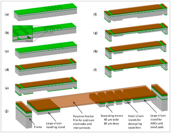
The process for the integration of electronic components into the neural implants starts with the accurate definition of silicon-based islands. Next, Parylene C is used to fabricate a flexible film connecting the predefined structures in silicon. Finally, the semi-flexible device is released using a DRIE process (Figure 1). Each of these steps is described in detail in the following subsections.

Figure 1.
Fabrication flowchart of the flexible device with 80 µm thick silicon islands integrated with parylene interconnects: (a) Deposition and patterning of the SiO2 mesh-shaped mask on an SOI substrate; (b) Definition of the silicon islands with trenches; (c) Sealing of the trenches with PECVD SiO2; (d) Deposition and patterning of the parylene film; (e) Etching of the advance in the bulk silicon; (f) Partial removal of the back-side SiO2 hard- etch mask; (g) Thinning the bulk silicon until the BOX stop layer; (h) Removing the exposed buried oxide layer; (i) Silicon islands thinning and device release; (j) The remaining BOX and SiO2 stop layer removal.
2.1. Precise Definition of the Electronic Components
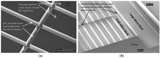
At the beginning of the fabrication process, number of silicon islands is precisely isolated by implementing a specially developed DRIE process for the fabrication of HAR embedded trenches [6]. First, a 2 µm thick PECVD SiO2 layer is deposited and patterned with submicron size slits to form a mesh-shaped hard mask on an SOI (Silicon On Insulator) wafer with desired device thickness (Figure 1a). Next, the silicon chips are precisely defined in a front-side DRI etch by high aspect ratio trenches using the buried oxide (BOX) as an etch-stop layer (Figure 1b and Figure 2a). The DRIE process was optimized in such a way that in one etch step narrow, individual trenches merge underneath the slits in the hard-etch mask to form large trenches defining the silicon islands. The slits in the remaining ~500 nm thin SiO2 mask are then sealed with a 2 µm layer of PECVD SiO2 (Figure 1c), which allows for further wafer scale processing.

Figure 2.
SEM images of the precisely defined 80 µm thick silicon islands: (a) Top view of the remaining SiO2 mesh-shaped mask after the trench front-side DRIE process; (b) Bottom view of the final device with separated small and large silicon islands after the back-side two-step DRIE release.
2.2. Fabrication of the Flexible Interconnection
At this stage, the silicon islands, which can contain almost any type of pre-fabricated active or passive components, are pre-defined in the SOI substrate by the buried trenches. After closure of the slits in the oxide hard-etch mask the surface of the wafer becomes fully planar again, allowing for the fabrication of the flexible interconnects that will mechanically and electrically connect the islands. In the full process flow these biocompatible interconnects would consist of platinum interconnects sandwiched in between two 5 µm thick layers of Parylene C [4]. In this short process flow demonstration the full stack has been replaced by a single 10 µm thick Parylene C film (Figure 1d).
2.3. Device Release and Thinning
The final step in the fabrication process is the device release and the thinning down of the silicon islands, which can serve as a miniature substrates for ASICs, passive components or bond pads for wire connections. In an optimized back-side DRIE process an advance is dry etched in the bulk silicon through a two-step PECVD SiO2 (Figure 1e). Next, part of the SiO2 hard-etch mask is etched away (Figure 1f) and consequent bulk thinning until the BOX stop layer is performed in the second DRIE step (Figure 1g). Then, the partially exposed buried oxide layer is removed (Figure 1h) and the final silicon substrate thinning and device release is simultaneously performed in the last silicon etch step (Figure 1i). Lastly, the landing BOX layer (ensuring the precise silicon islands thickness) and the SiO2 layer deposited while closing the trenches are etched away. The flexible device with 80 µm thick silicon islands integrated with parylene interconnects is formed (Figure 1j and Figure 2b).
3. Results and Discussion
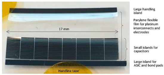
We have successfully combine the key fabricate steps to manufacture a 11 mm wide, 18 mm long and 80 µm thick proof of concept device (Figure 3) composed of:

Figure 3.
Top-view photography of the 80 µm thin released device composed of small (2.000 µm × 200 µm) and large (17 mm × 1 mm and 18 mm × 1.1 mm) silicon islands separated by 40 µm wide trenches and connected with the 10 µm thick parylene-based flexible interconnect.
- 128 small silicon islands (2 mm × 200 µm), defined with the 40 µm wide trenches, that in the final implant will contain high density AC decoupling capacitors for stimulation electrodes.
- 2 large silicon islands (17 mm × 1 mm and 18 mm × 1.1 mm), which can accommodate an ASIC, contain bond pads for wire bonding or allow for device handling during assembly.
- 10 µm thick parylene film, which at the same time connects the multidimensional silicon islands and can contain flexible stimulation electrodes in the large flexible area (17 mm × 5 mm).
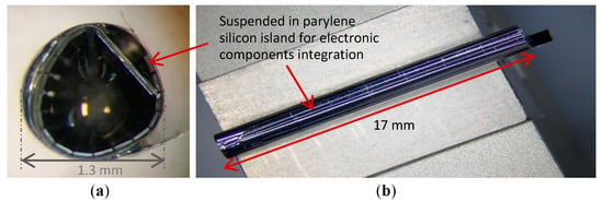
The fine level of silicon wafer segmentation, and component connection with the parylene film, ensures the device flexibility and enables its wrapping (see Video S1) into an 18 mm long cylindrical structure with a diameter of only 1.3 mm (Figure 4). The cylinder will eventually form the active electrode tip of a Deep Brain Stimulation probe.

Figure 4.
Photography of the 10 mm wide and 17 mm long device, with integrated various-size silicon island, wrapped into a 1.3 mm diameter needle-like shape: (a) Cross-section of the device with 200 µm wide small silicon islands suspended in parylene film; (b) Side-view of the 17 mm long needle-shape device.
4. Conclusions
We have presented a technology concept that can serve as an integration and assembly platform for minimally invasive implantable devices. In the concept, silicon islands of arbitrary shapes and thickness are connected by flexible platinum interconnects sandwiched in between two parylene layers. The technology concept is validated with a non-functional demonstrator presented in this paper. The successful fabrication and rolling of this device into a DBS probe-shape structure proves feasibility of the concept. Further steps comprise the inclusion of the platinum interconnects and the fabrication of the stimulation electrodes.
Supplementary Materials
The video of the device wrapping is available online at https://vimeo.com/280543670 (Password: wrapping)–Video S1: Wrapping of the semi-flexible parylene-silicon based implantable device.
Author Contributions
M.K. and R.D. conceived and designed the experiments; M.K. performed the experiments and analyzed the data; A.S., H.v.Z. and G.P. contributed in developing and optimizing the fabrication process; M.K., B.M. and R.D. wrote and structured the paper.
Funding
This research and resulting paper were carried on within InForMed project funded by ECSEL JU grant no: 2014-2-662155.
Acknowledgments
The experiments and measurements were conducted in the Else Kooi Laboratory—CL100 cleanroom facility. Further, we would like to acknowledge Wim Weekamp from Philips Research, Eindhoven (NL) for designing the wrapping tool and performing the first device assembly.
Conflicts of Interest
The authors declare no conflict of interest. The founding sponsors had no role in the design of the study; in the collection, analysis, or interpretation of data; in the writing of the manuscript, and in the decision to publish the results.
References
- Lago, N.; Cester, A. Flexible and Organic Neural Interfaces: A Review. Appl. Sci. 2017, 7, 1292. [Google Scholar] [CrossRef]
- Seymour, J.; Wu, F.; Wise, K.D.; Yoon, E. State-of-the-art MEMS and microsystem tools for brain research. Microsyst. Nanoeng. 2017, 3, 16066. [Google Scholar] [CrossRef] [PubMed]
- Gad, P.; Choe, J.; Nandra, M.S.; Zhong, H.; Roy, R.R.; Tai, Y.C.; Edgerton, V.R. Development of a multi-electrode array for spinal cord epidural stimulation to facilitate stepping and standing after a complete spinal cord injury in adult rats. J. Neuroeng. Rehabil. 2013, 10. [Google Scholar] [CrossRef] [PubMed]
- Barz, F.; Lausecker, R.; Wallrabe, U.; Ruther, P.; Paul, O. Wafer-level shellac-based interconnection process for ultrathin silicon chips of arbitrary shape. In Proceedings of the 2016 IEEE 29th International Conference on Micro Electro Mechanical Systems (MEMS), Shanghai, China, 24–28 January 2016; pp. 520–523. [Google Scholar]
- Schander, A.; Tolstosheeva, E.; Biefeld, V.; Kempen, L.; Stemmann, H.; Kreiter, A.; Lang, W. Design and fabrication of multi-contact flexible silicon probes for intracortical floating implantation. In Proceedings of the 2015 Transducers–2015 18th International Conference on Solid-State Sensors, Actuators and Microsystems (TRANSDUCERS), Anchorage, AK, USA, 21–25 June 2015; pp. 1739–1742. [Google Scholar]
- Kluba, M.; Arslan, A.; Stoute, R.; Muganda, J.; Dekker, R. Single-Step CMOS Compatible Fabrication of High Aspect Ratio Microchannels Embedded in Silicon. Proceedings 2017, 1, 291. [Google Scholar] [CrossRef]
Publisher’s Note: MDPI stays neutral with regard to jurisdictional claims in published maps and institutional affiliations. |
© 2018 by the authors. Licensee MDPI, Basel, Switzerland. This article is an open access article distributed under the terms and conditions of the Creative Commons Attribution (CC BY) license (https://creativecommons.org/licenses/by/4.0/).