1. Introduction
Monitoring the strength of static and quasistatic electric fields (E-field) is key for many scientific and industrial purposes, e.g., improving the reliability of weather forecast, researching charge distributions in cloud systems or safety in the vicinity of high-voltage infrastructure. Despite this high demand, as of yet, there exist no state-of-the-art sensors which are sufficiently capable of fulfilling this task. This is either due to the necessity for grounded components which severely distort the E-field (field mills [
1,
2]), large temperature dependence (electrooptical sensors [
3,
4]) or limited bandwidth (antennae [
5,
6]). Recently, a new transduction scheme for the electric field strength was presented which does not suffer from these drawbacks [
7].
This transduction exploits the electrostatic induction occurring in conducting bodies inside an electric field
. The surface charges arising due to the induction are themselves subject to
leading to a force
proportional to
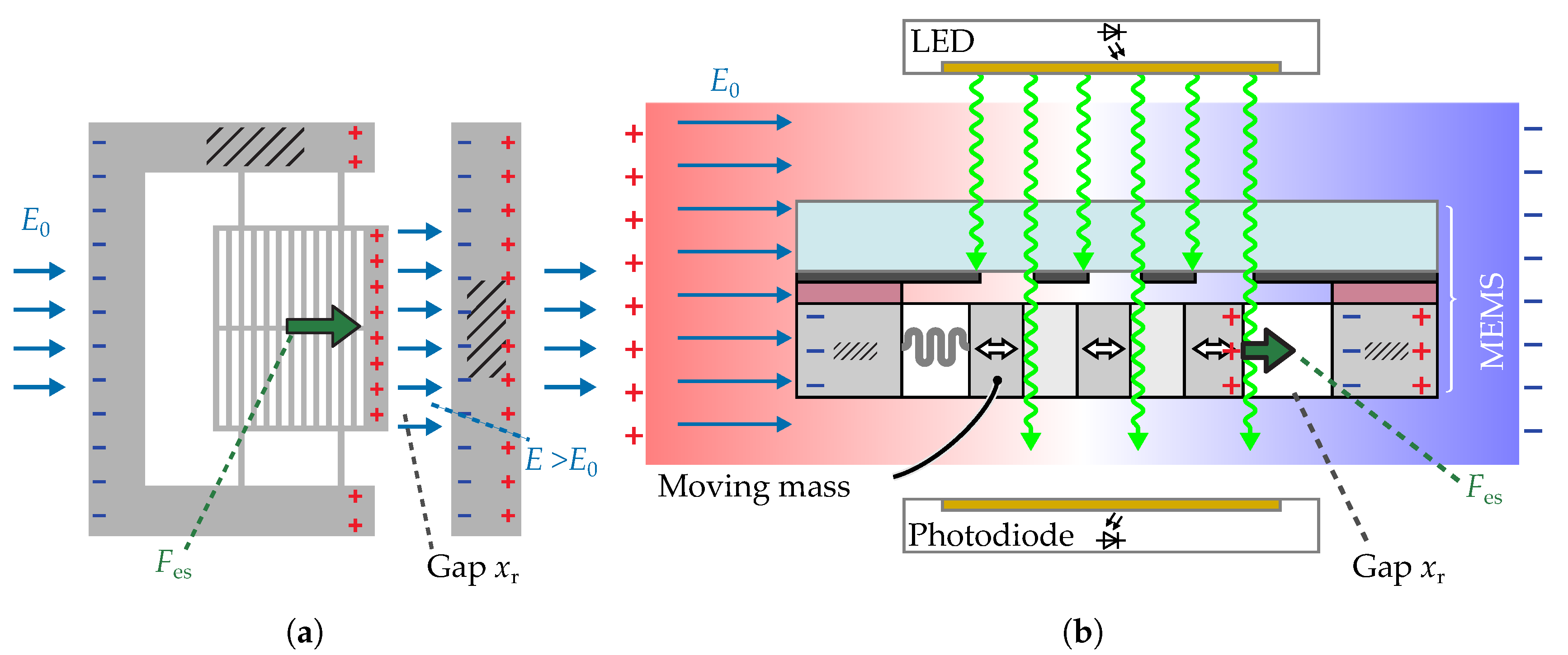
. The MEMS sensors are designed such that the electric field is concentrated across a narrow gap separating a moveable silicon mass from a fixed Si part (
Figure 1a), which increases
. The force leads to a displacement of the Si mass which is read out optically.
This is achieved by light flux modulation with an optical shutter (
Figure 1b). The optical shutter is composed of a Cr grid deposited on a glass chip and an identical grid etched into the moving mass of the Si chip. Thus, light which is introduced onto the top side of the sensor chip is modulated by the mass displacement caused by the electric field. This kind of readout has proven to be highly sensitive [
8,
9].
Since the E-feld transduction scheme is new, little is known about its properties. Making use of an equivalent circuit model helps understanding a few basic characteristics and provides a qualitative understanding.
2. Model
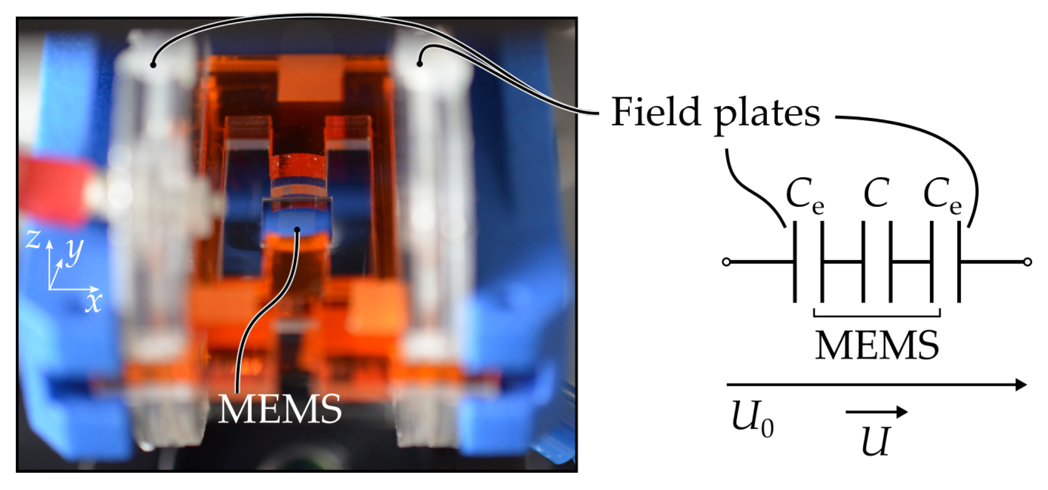
The equivalent circuit model of the sensor’s frequency-dependent transfer function
presented here encompasses not only the sensor chip but also parts of the measurement setup. These parts are the capacitor plates used to provide the electric field to the MEMS. As depicted in
Figure 2, the field plates of the experimental setup and the MEMS chip can be understood as three capacitors connected in series.
The first capacitor comprises one of the aluminum plates and the opposing side face of the device layer of the MEMS chip. The second capacitor
C corresponds to the sensing gap of the MEMS chip and the third capacitor encompasses the remaining aluminum plate and opposing face of the MEMS chip. Since the chip is placed in the centre of the setup and the dimensions of the plates are the same, it follows with sufficient accuracy that the external capacitances are the same, i.e.,
. The voltage
applied to this voltage divider corresponds to the voltage which generates the electric feld
to be measured, where
is the distance between the field plates. The force picked up by the sensor corresponds to the square of the voltage drop
U at
C, i.e.,
, where
is the characteristic of the capacitive voltage divider which can be calculated as the fraction of the impedance of the sensing gap
over the total impedance
,
This expression is independent from
and, thus, constant. Equation (
1) corresponds to the ideal case, i.e., perfect conductance of the Si and infinite resistance of the gap between. Furthermore, it reveals that a low ratio
is in favour of a large voltage drop across
C and, thus, a large force
.
This approach can also be used to explore what happens, if a parasitic resistance
in parallel to
C occurs. The impedance of a resistor in parallel with a capacitor is given as
. The corresponding voltage drop over the sensing capacitor is, therefore, proportional to the characteristic
In contrast to the ideal case Equation (
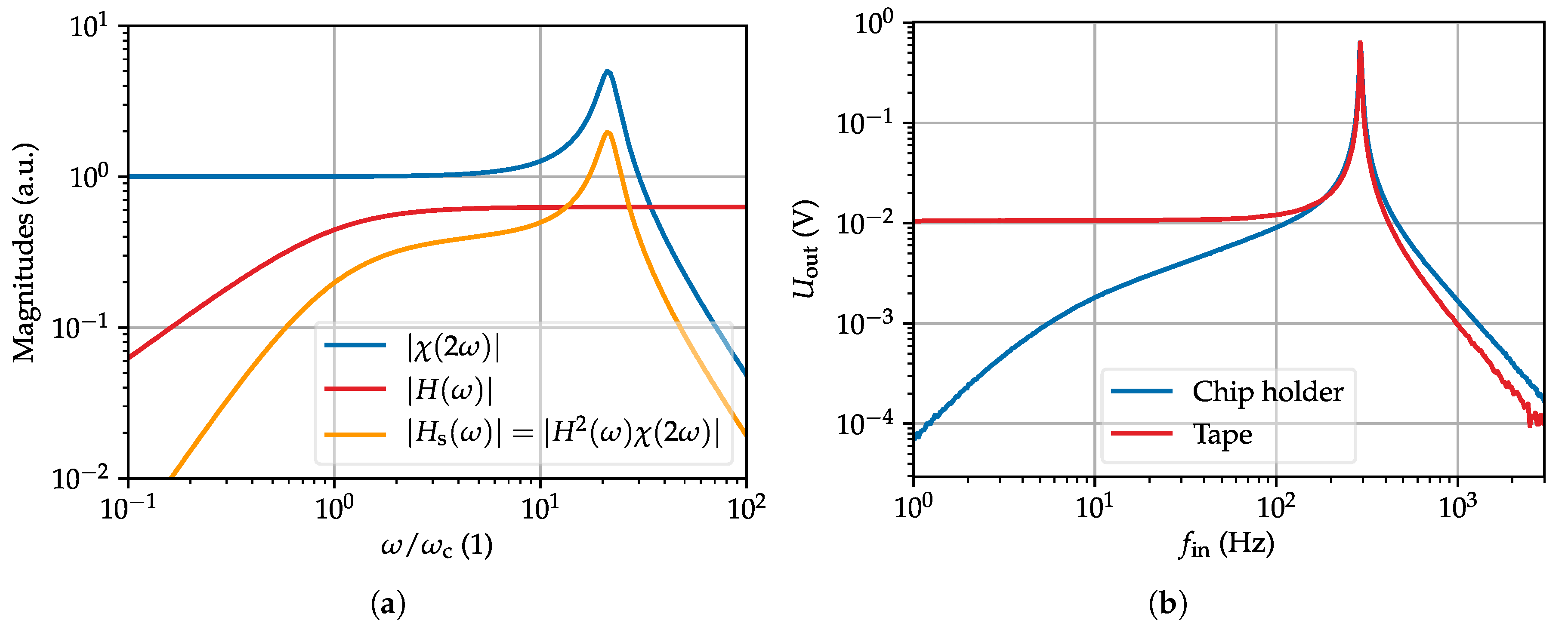
1), this expression is frequency dependent. It corresponds to a first order high-pass with corner frequency
.
It can be seen that a finite parasitic resistance severely affects the E-feld transduction for low frequencies and DC. In particular, the bandwidth becomes clipped for frequencies
. Note that
enters the transfer function quadratically,
, where
corresponds to the mechanical characteristic of the MEMS [
7,
10]. Therefore, the linear increase of
reflects in a quadratic increase in
worsening the circumstance (see
Figure 3).
3. Results
The above described parasitic effect was encountered during the first measurements with the sensor. The model helped to identify its source as the plastic chip holder which introduced a resistance across the sensing gap (see
Figure 3).
Estimating the capacitances C and from the geometry of MEMS and field plates and the corner frequency Hz from the measured data, it was possible to roughly quantify the value of . The distance between the plate and the chip face is given by mm. The mean area of the external capacitor can be estimated by cm2. Therefore, the external capacitance roughly has a value of pF.
The capacitance C of the sensing gap can be estimated in a similar manner and has around pF for a 10 µm gap. This yields a parasitic resistance of G. Even though this value is quite large, the effect was clearly noticeable. Therefore, the choice of mounting the MEMS chip is crucial for proper measurements.
4. Conclusions
A very simple equivalent circuit model of an optomechanical MEMS electric field sensor was presented. The model also encompasses the effects of a parasitic resistor. This way it was possible to explain and identify the source of the reduced sensitivity of the sensor at low frequencies. The model can be expanded easily to account for, e.g., the finite condictance of Si.
Acknowledgments
This work was supported by the country of Lower Austria (NÖ, the European Regional Development Fund (ERDF) and the Austrian Science Fund (FWF project number P 28404-NBL).
Conflicts of Interest
The authors declare no conflict of interest. The founding sponsors had no role in the design of the study; in the collection, analyses, or interpretation of data; in the writing of the manuscript, and in the decision to publish the results.
References
- Hill, D.A.; Kanda, M. The Measurement, Instrumentation, and Sensors Handbook XXV, Section 47, Electric Field Strength; CRC Press LLC: Boca Raton, FL, USA; IEEE Press: Piscataway, NJ, USA, 1999. [Google Scholar]
- Kirkham, H. On the measurement of stationary electric fields in air. In Proceedings of the Conference on Precision Electromagnetic Measurements, Ottawa, ON, Canada, 16–21 June 2002. [Google Scholar]
- Chmielak, B.; Waldow, M.; Matheisen, C.; Ripperda, C.; Bolten, J.; Wahlbrink, T.; Nagel, M.; Merget, F.; Kurz, H. Pockels effect based fully integrated, strained silicon electro-optic modulator. Opt. Express 2011, 19, 17212–17219. [Google Scholar] [CrossRef] [PubMed]
- Perry, D.; Chadderdon, S.; Gibson, R.; Shreeve, B.; Selfridge, R.H.; Schultz, S.M.; Wang, W.C.; Forber, R.; Luo, J. Electro-optic polymer electric field sensor. In Proceedings of the SPIE Smart Structures and Materials+ Nondestructive Evaluation and Health Monitoring, San Diego, CA, USA, 6–10 March 2011; International Society for Optics and Photonics: Bellingham, WA, USA, 2011; p. 79820. [Google Scholar]
- Roussy, G.; Agbossou, K.; Dichtel, B. Vector electric field measurement using a non-interfering sensor. Meas. Sci. Technol. 2000, 11, 1145. [Google Scholar] [CrossRef]
- Chiang, F.C.; Pribyl, P.; Gekelman, W.; Lefebvre, B.; Chen, L.J.; Judy, J.W. Microfabricated flexible electrodes for multiaxis sensing in the large plasma device at UCLA. IEEE Trans. Plasma Sci. 2011, 39, 1507–1515. [Google Scholar] [CrossRef]
- Kainz, A.; Steiner, H.; Schalko, J.; Jachimowicz, A.; Kohl, F.; Stifter, M.; Beigelbeck, R.; Keplinger, F.; Hortschitz, W. Distortion-free measurement of electric field strength with a MEMS sensor. Nat. Electron. 2018, 1, 68. [Google Scholar] [CrossRef] [PubMed]
- Hortschitz, W.; Steiner, H.; Stifter, M.; Kohl, F.; Kahr, M.; Kainz, A.; Raffelsberger, T.; Keplinger, F. Novel high resolution MOEMS inclination sensor. In Proceedings of the IEEE SENSORS 2014 Proceedings, Valencia, Spain, 2–5 November 2014; pp. 1893–1896. [Google Scholar] [CrossRef]
- Middlemiss, R.; Samarelli, A.; Paul, D.; Hough, J.; Rowan, S.; Hammond, G. Measurement of the Earth tides with a MEMS gravimeter. Nature 2016, 531, 614–617. [Google Scholar] [PubMed]
- Kainz, A.; Hortschitz, W.; Steiner, H.; Schalko, J.; Jachimowicz, A.; Keplinger, F. Accurate analytical model for air damping in lateral MEMS/MOEMS oscillators. Sens. Actuators A Phys. 2017, 255, 154–159. [Google Scholar] [CrossRef]
| Publisher’s Note: MDPI stays neutral with regard to jurisdictional claims in published maps and institutional affiliations. |
© 2018 by the authors. Licensee MDPI, Basel, Switzerland. This article is an open access article distributed under the terms and conditions of the Creative Commons Attribution (CC BY) license (https://creativecommons.org/licenses/by/4.0/).

 ,
, 