Proceeding Paper

Silicon-On-Nothing IR-Emitter for Gas Sensing Applications †

by
Vladislav Komenko
1,*,
Andrey Kravchenko
1 and
Wolf-Joachim Fischer
2
1
Infineon Technologies Dresden GmbH, 01099 Dresden, Germany
2
Institute of Semiconductors and Microsystems, TU Dresden, 01187 Dresden, Germany
*
Author to whom correspondence should be addressed.
Presented at the Eurosensors 2018 Conference, Graz, Austria, 9–12 September 2018.
Proceedings 2018, 2(13), 1080; https://doi.org/10.3390/proceedings2131080
Published: 20 November 2018
(This article belongs to the Proceedings of EUROSENSORS 2018)

Abstract

:
Within the current work, we present a miniaturized IR-Emitter based on Silicon-On-Nothing (SON) technology capable of producing 10 ms pulses. Transition to monocrystalline silicon, as the material choice for the filament, is governed by improved reliability and greater thermal stability as opposed to polycrystalline silicon alternative, commonly used in such class of devices. Compact design, low-cost processing and exceptional filament material properties make the presented device a favorite solution for integrated gas sensing applications. Numerical modeling and measurements of the IR-Emitter are performed to investigate the heating dynamics and assess the structure’s behavior at extreme temperatures as well as confirm the target performance. Additionally, a part of the work is dedicated to cover the insight of used fabrication process and the discussion of further improvements.

1. Introduction

In recent times, the consumer market has been rapidly expanding in the direction of gas sensing. Robust, cost effective and compact solutions are currently a topic of research and development. A series of promising detection approaches rely on the ability of gases to absorb radiation within the visible and near infrared ranges [1,2,3]. Taking that into consideration, the focus of this work is on modeling and characterization of an IR-Emitter capable of 10 ms pulsed operation. Proposed device relies on an innovative approach of structuring the heated element in a crystalline silicon membrane, formed by the Silicon-On-Nothing (SON) process. In principle, such material choice should be more reliable and thermally stable compared to a polysilicon solution yet shares the same wide list of front-end processing options as opposed to silicides and metal films [4]. This is critical to allow direct compatibility and integration into the standard CMOS process for further cost reduction.

2. Materials and Methods

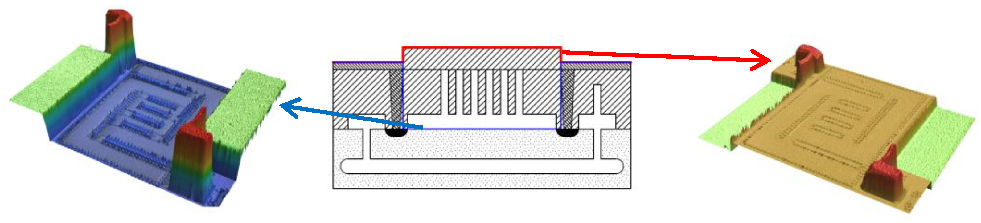
2.1. Geometry and Setup
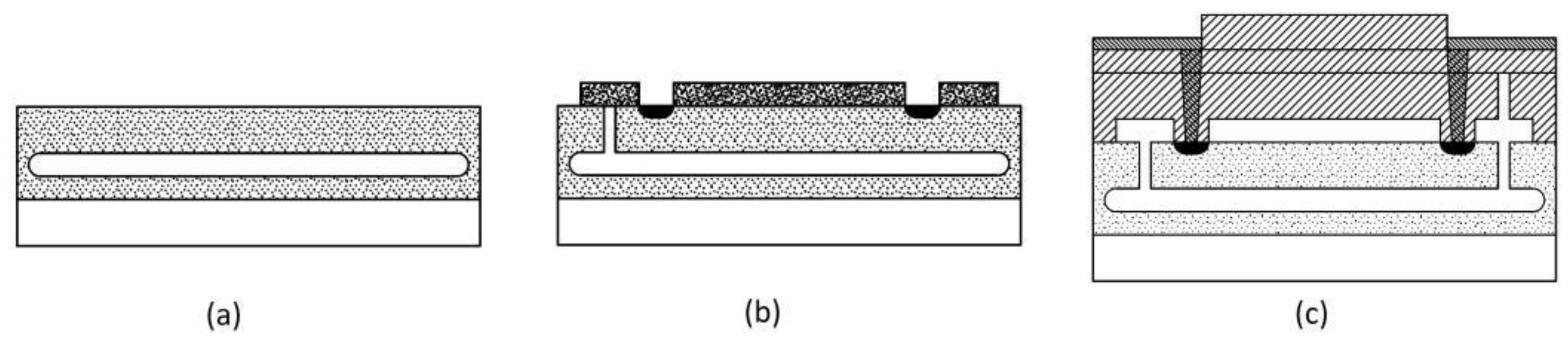
General geometry of the device represents a meander-shaped filament supported by cantilevers on the sides. To improve thermal isolation the micro-bulb concept was used, where bottom and top cavities formed by means of the SON process and a sacrificial layer respectively, allow mechanical and electrical decoupling from the bulk with only an oxide bridge connection at the base of the cantilevers. Figure 1 represents (a) the model used for heat transfer simulations by means of finite elements method (FEM), (b) the integrated device and (c) glowing filament.
Main thermal loss sources include contacts, supports and losses through air. The latter is optimized by encapsulation of heating element and lowering the pressure within the cavity. Full sealing of the IR-Emitter allows the device to be operated independent of the ambient conditions.

2.2. Manufactering

Key manufacturing steps are presented in Figure. Fabrication follows the standard SON process, where a monocrystalline membrane and bottom cavity are formed. Additionally, a blanket implant was added to adjust the electrical properties of the membrane (Figure 2a). A double deep silicon trench etch concept is used to structure the emitter filament. After etching the first trench, small fixing points are left to prevent the structure from bending due to mechanical stresses during later processing. To form the top cavity a sacrificial layer is used, what is schematically shown in Figure 2b. Openings in the sacrificial layer define the filament fixing points, contact areas and positions of the lid supporting pylons.
Due to low infrared absorption, a CVD-Oxide is used as main material for encapsulation of the device. After the lid deposition directly on the patterned sacrificial layer, the structure of IR-Emitter is fixed and second deep trench etch can be applied. Trench pattern complements the geometry used by the first etch. As a result, filament is fully electrically decoupled from the substrate. Mechanical stability to the assembly is still provided by the sacrificial layer. After deposition of the sealing, back-end processing included a contact etch with a TiN/Ti liner deposition and tungsten filling. For metal interconnects aluminium is chosen. Figure 2c shows final fabrication steps consisting of plasma etch of the sacrificial layer to release the structure, sealing with an additional oxide layer and a pad open step to enable electrical access. A 3D-profile of the final geometry presented in Figure 3, indicates no initial bending of the filament and minimized deformation of the lid.

3. Results

3.1. Electrical Characterization

Manufactured structures were subjected to electrical measurements to assess the performance. A constant voltage was applied to first investigate the behavior of the emitter at a fixed load. As expected, while applying more power to the structure, the sample heats up. Due to phonon scattering effects, the mobility and in turn the conductivity of the filament decreases. It can be observed in Figure 4a how the tendency changes once the input power reaches 70 mW. At such high temperatures, intrinsic conductivity plays a dominant role. As a result, resistance drops.
To confirm the ability of the emitter to support pulsed operation, a transient characterization was performed. Voltage was applied in 10 ms pulses and the input power was monitored to assess the heating dynamic. During ramp up, as can be seen in Figure 4b, the emitter is capable of reaching the target operation point within 5 ms for 18 V applied. This is indicated by the settled power consumption in the on-state. During the cooling cycle, thermal losses enable fast structure recovery. Both of the measurements are in good agreement with the expectations set by the device modelling.

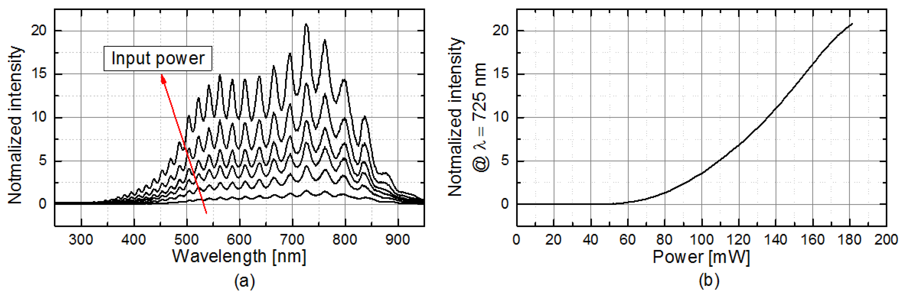
3.2. Optical Characterization

The device is intended to operate as an IR-Emitter; therefore, the spectral response and the radiated power are key parameters. It can be seen in Figure 5a, how the radiated intensity increases with more current passing through the structure. A cut along the 725 nm wavelength, available in Figure 5b, shows a steady increase in radiated power with a slope decreasing after 170 mW. The latter is associated with increased losses due to a shift in the heat generation closer to the mechanical supports. This originates from the fact that the filament becomes more electrically conducting, which results in more voltage drop over the cantilevers. Power starts dissipating in areas that also exhibit greater thermal losses, this lowers the total efficiency. Contact material has to be chosen appropriately to withstand this heating. Similarly, the curve indicates that a minimal power of 70 mW is required for operation.

4. Discussion

After investigating the spectrum presented previously in Figure 5a one can note an interference pattern. In an attempt to explain such spectral behavior, transmission of the top cavity and the oxide lid (see Figure 6a) is calculated. The spectral profile clearly indicated that the top lid is responsible for the observed interference. This opens a possibility for direct filter integration on the emitter. A separately manufactured filter response is given in Figure 6b.
In the current work, we presented an IR-Emitter with crystalline silicon as the material for the filament. Device was fabricated based on the SON technology and was proven to be capable of 10 ms pulsed operation. Investigation of the radiated spectrum shows a possibility of filter integration directly on the emitter. This enables further miniaturization and cost reduction of gas-sensing systems, where the light of a certain band is of interest. Such systems might significantly benefit from an integrated solution as opposed to typically used discrete components.

Author Contributions

A.K. and V.K. contributed to concept development and paper writing. A.K. performed the numerical modeling and device characterization while V.K. worked on processing and fabrication topics. W.-J.F. supported and guided the work.

Funding

this research was funded by Infineon Dresden GmbH.

Acknowledgments

Technical and resource support of Infineon Dresden GmbH is gratefully acknowledged.

Conflicts of Interest

The authors declare no conflict of interest. The founding sponsors had no role in the design of the study; in the collection, analyses, or interpretation of data; in the writing of the manuscript, and in the decision to publish the results.

References

  1. Qian, K.; Li, F.; Cheng, M.; San, H.; Chen, X. MEMS Infrared emitter based on SOI wafer. Acta Opt. Sin. 2010, 30, 1455–1458. [Google Scholar] [CrossRef]
  2. San, H.; Li, C.; Chen, X.; Chen, R.; Zhang, Q. Silicon-Based Micro-Machined Infrared Emitters with a Micro-Bridge and a Self-Heating Membrane Structure. IEEE Photonics Technol. Lett. 2013, 25, 1014–1016. [Google Scholar] [CrossRef]
  3. Schjølberg-Henriksen, K.; Gjessing, J.; Bakke, K.A.H.; Hadzialic, S.; Wang, D.T. Miniature, low-cost, 200 mW, infrared thermal emitter sealed by wafer-level bonding. In Proceedings of the SPIE 10108, Silicon Photonics XII; Event: SPIE OPTO: San Francisco, CA, USA, 2017. [Google Scholar] [CrossRef]
  4. Reggiani, S.; Valdinoci, M.; Colalongo, L.; Rudan, M.; Baccarani, G.; Stricker, A.D.; Illien, F.; Felber, N.; Fichtner, W.; Zullino, L. Electron and hole mobility in silicon at large operation temperatiures. I. Bulk mobility. AIEEE Trans. Electron Devices 2002, 49, 490–499. [Google Scholar] [CrossRef]
Figure 1. (a) FEM analysis of heat distribution within emitter structure, (b) optical image of produced device, (c) IR-Emitter at operation mode.
Proceedings 02 01080 g001
Figure 2. Schematic drawing of device cross section after (a) SON-process, (b) deposition of sacrificial layer over the first trench and (c) suspended structure after sacrificial layer was removed.
Proceedings 02 01080 g002
Figure 3. 3D scan over the filament (left) and lid surface (right) made by means if lase microscopy.
Proceedings 02 01080 g003
Figure 4. Simulated an measured response for (a) constant load and at (b) pulsed operation.
Proceedings 02 01080 g004
Figure 5. (a) Normalized emitted spectrum of structure at different input power, (b) normalized intensity at 725 nm wavelength.
Proceedings 02 01080 g005
Figure 6. (a) Simulated transmission spectrum of the cavity/Oxide lid stack, (b) proposed filter.
Proceedings 02 01080 g006
Publisher’s Note: MDPI stays neutral with regard to jurisdictional claims in published maps and institutional affiliations.

