Abstract
We present new developments of CMOS compatible direct conversion terahertz detector operating at room temperature. The rectenna consists of an integrated antenna, realized on the surface of the integrated circuit and connected to a nanometric metallic whisker at one of its edges. The rectifying device can be obtained introducing just minor modifications of the charge storage well in conventional CMOS active pixel image sensor devices, making the proposed solution easy to integrate with existing imaging systems. In the paper we present technological developments of the rectifier structure, realized with minor changes from a standard 0.15 µm technology node. We also present the study of a patch antenna which can be directly integrated on the chip.
1. Introduction
THz imaging and spectroscopy applications have a great potential in time-domain spectroscopy, communications, security control, and biomedical imaging. For this reason, in past decades a great interest of the research community has been attracted by this region of the electromagnetic spectrum, pushing the microwave and optical THz devices through a constant progress in the development and the improvement of detectors in terms of noise equivalent power.
Recently we presented a new approach to the THz detectors resulting from the direct integration of the antenna with a rectifying device obtained by modification of commercial CMOS active pixel image sensor (APS) [1,2]. We demonstrated that a modification of a limited region of the surface of the Storage Well (SW), placed in contact with metal whisker, constituting an edge of the antenna, results in an efficient rectifying device, with no need to rely on deep submicron technology, Figure 1. The antenna and the rectifying device forma a “rectenna” structure which, exposed to electromagnetic radiation, gives rise to charge injection into the SW. The charge can be collected during the integration time. The rectifying structure is realized by the metal of a via contact, placed at the base of the antenna, in contact with a p+ doped semiconductor. A second junction is formed by the by p+ doped surface layer and n doped layer of the SW.
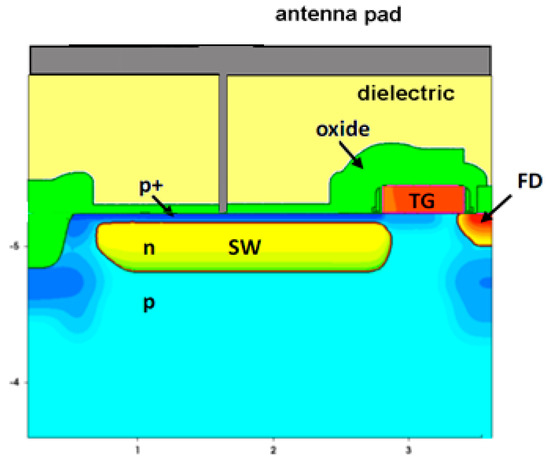
Figure 1.
Sketch of the detector structure.
In this paper we report about further steps into the development of the THz rectifier in particular of the possibility to reduce electronic defects at the surface of the semiconductor in correspondence of the contact with the metal whisker by interposing a thin silicon rich oxide layer.
2. Realization and Characterization of the Rectifyer
The structure of the THz rectifier re-use most of a conventional CMOS APS, making the proposed solution easy to integrate with existing imaging systems. In particular, the THz rectifier here presented was obtained using OnSemi (CIS) 0.15 µm technology.
In CMOS APS device, a n-doped SW is embedded within a p doped substrate [3]. A Transfer gate transistor (TG) allows the extraction of the charge accumulated in the SW, after an integration time. An additional p+ implantion is commonly used in a CMOS APS to separate the low n-doped SW from the semiconductor surface.
A sketch of the detector structure is reported in Figure 1. The rectifying device is created at the base of a nano-whisker using its metal edge as spart of the electronic device itself. The metal/p+ silicon, form a first Shottcky barrier, the p+/n semiconductor junction forms a second barrier. The p+ layer is completely depleted, thus a joint double barrier structure is formed, with vertical extension of some tenths of nanometers. This structure is an effective rectifying device and enables excellent maintenance of the barrier surrounding the SW [1].
An additional implantation in the p+ zone just below the whisker base, parameters reported in Table 1, was performed in order to achieve a sharper structure.

Table 1.
Doping implantation parameters.
In the present paper we report results with a metal whisker optimized with the addition of a SiOx layer, 70 Å thick, interposed between the metal and the semiconductor, as sketched in Figure 2. SiOx blokes the penetration of metal toward the semiconductor, dramatically reducing interface defects and spurs electrons injection [4]. The layer thickness is evaluated in order to correctly allow penetration of electric field from the antenna. DC conduction of the rectified current is also maintained, by hopping between the defects in the SiOx layer [5].
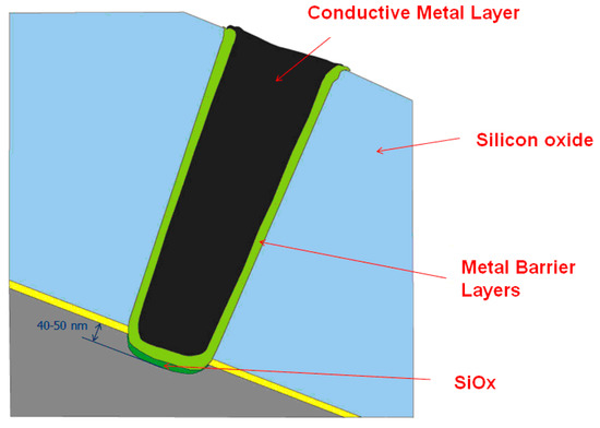
Figure 2.
Schematic section of the standard via contact of CMOS technology, adapted for the THz rectifier as the metal whisker at the bottom of the antenna, forming the rectifier junction.
Measurements where performed at 1 GHz and 40 GHz, and are reported in Figure 3. The variables k refer to the slopes of the curves, which must be considered in the NEP calculation. Following the procedure presented in [1] we obtained the evaluation at 1 THz of NEP = 28 pW/Hz1/2, value which substantially improve former results.
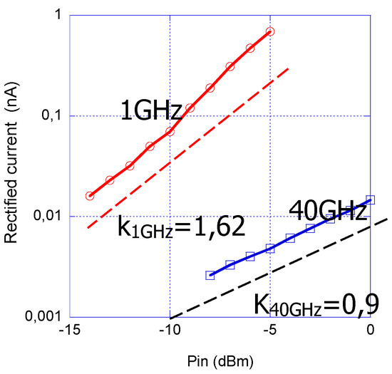
Figure 3.
Rectified current versus applied power for sample B27.
3. Study of the Patch Antenna
The project of a planar antenna, realized directly shaping the metal layers available in the CMOS technology, is here presented. The antenna can have a structure of a patch antenna, constituted by a square of dimension 80 μm × 80 μm. The semiconductor p+ doped layer constitutes the ground plane.
The square patch is surrounded by a metal plane, connected to the p+ ground plane by a series of via contacts. For this particular, the structure obtained can also be considered as a slab antenna.
A DC connection between the antenna pad ad ground must be ensured. In Figure 4 the ground connection is placed on left side of the patch, while the whisker, and the rectifying junction at its bottom, are located on the opposite side.
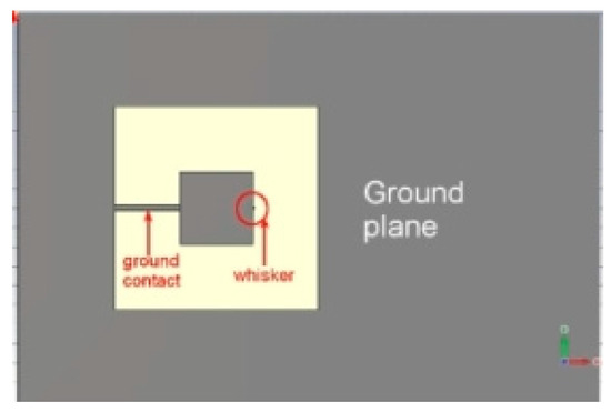
Figure 4.
New patch antenna which can be directly integrated on the surface of the CMOS chip.
This approach has intrinsically lower capability to concentrate the electric field onto the whisker edge, with respect to the 3D architecture formerly proposed in [6], nevertheless it offers the possibility of easier realization, at lower cost, directly within the CMOS fabrication process.
A CST simulation of the structure is shown in Figure 5. In this case for the realization of the antenna is assumed to use the first metal layer of the CMOS technology, thus at a distance from the substrate of only 500 nm. Simulation shows the Field Enhancement factor, defined as the ratio between the amplitudes of the Electric field below the whicker and the Electric field of the incident wave, results to be still very high.
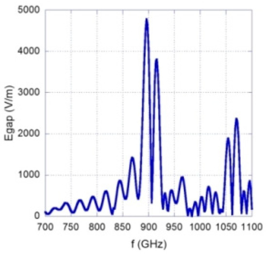
Figure 5.
Electromagnetic simulations which indicate the high Field Enhancement which can be achieved by the planar antenna.
4. Conclusions
We presented new results of the rectification capability of the double barrier semiconductor structure realized with the presence of a Silicon rich oxide layer. The presence of this additional layer do not reduce the rectification capability, rather a lower NEP was fond. The design of a new structure of planar antenna, compatible with CMOS technology was also presented.
Conflicts of Interest
The authors declare no conflict of interest.
References
- Varlamava, V.; De Amicis, G.; Del Monte, A.; Perticaroli, S.; Rao, R.; Palma, F. CMOS-Compatible Room-Temperature Rectifier Toward Terahertz Radiation Detection. J. Infrared Millim. Terahz Waves 2016, 37, 737. [Google Scholar] [CrossRef]
- Varlamava, V.; Palma, F.; Nenzi, P.; Balucani, M. Electric Field Enhancement in 3-D Tapered Helix Antenna for Terahertz Applications. IEEE Trans. Terahertz Sci. Technol. 2014, 4, 360–367. [Google Scholar] [CrossRef]
- Fossum, E.R.; Hondongwa, D.B. A Review of the Pinned Photodiode for CCD and CMOS Image Sensors. IEEE J. Electron Devices Soc. 2014, 2, 33–43. [Google Scholar] [CrossRef]
- Rao, R.; Simoncini, R.; Irrera, F. Trapping in high-k dielectrics. Appl. Phys. Lett. 2010, 97, 163502. [Google Scholar] [CrossRef]
- Rao, R.; Irrera, F. Threshold Voltage Instability in High-k Based Flash Memories. Microelectron. Reliab. 2010, 50, 1273–1277. [Google Scholar] [CrossRef]
- Nenzi, P.; Tripaldi, F.; Varlamava, V.; Palma, F.; Balucani, M. On-Chip THz 3D Antennas. In Proceedings of the 2012 IEEE 62nd Electronic Components and Technology Conference (ECTC), San Diego, CA, USA, 29 May–1 June 2012; pp. 102–108. [Google Scholar]
Publisher’s Note: MDPI stays neutral with regard to jurisdictional claims in published maps and institutional affiliations. |
© 2017 by the authors. Licensee MDPI, Basel, Switzerland. This article is an open access article distributed under the terms and conditions of the Creative Commons Attribution (CC BY) license (https://creativecommons.org/licenses/by/4.0/).