Article

Design, Modeling, and Implementation of Dual Notched UWB Bandpass Filter Employing Rectangular Stubs and Embedded L-Shaped Structure

1
School of Information Science and Engineering, NingboTech University, Ningbo 315104, China
2
College of Information Science and Electronic Engineering, Zhejiang University, Hangzhou 310027, China
3
College of Electronics and Information Engineering, Nanjing University of Aeronautics and Astronautics (NUAA), Nanjing 210000, China
4
Department of Electrical Engineering, University of Engineering and Technology, Peshawar 25000, Pakistan
*
Author to whom correspondence should be addressed.
Fractal Fract. 2023, 7(2), 112; https://doi.org/10.3390/fractalfract7020112
Submission received: 18 December 2022 / Revised: 19 January 2023 / Accepted: 20 January 2023 / Published: 23 January 2023

Abstract

:
Targeting the range defined by the FCC (Federal Communication Commission) in 2002 for ultra-passband bandpass filters, i.e., 3.1 to 10.6 GHz, this article presents a simple compact multipoles ultra-wideband bandpass filter (range starting from 2.9 GHz and end at 11.5 GHz with central frequency 7.2 GHz) using parallel coupled microstrip line and multimode resonator with controllable double narrow notched bands at 3.5 GHz and 7.5 GHz by embedded a spur line structure and rectangular stub resonator coupled to the middle section of the multimode resonator to eliminate the interference with the existing radio signals falls in the range of 3.1 to 10.6 GHz, respectively. After optimization of the proposed filter, some attractive features were obtained, i.e., a compact size 21 mm × 5.2 mm, simple topology, good reflection coefficient lower than −18 dB, good passband transmission coefficient –1.1 dB over the entire fractional bandwidth of about 119.4%, and four transmission poles at 3.4 GHz, 4.6 GHz, 6.5 GHz, and 10 GHz, respectively, can be seen which improves the performance of the filter. Finally, the fabricated filter was tested, and the results obtained demonstrated an excellent agreement.

1. Introduction

A regulated unlicensed spectrum (3.1 GHz to 10.6 GHz) belongs to a family IEEE (Institute of Electrical and Electronics Engineers) 802.15.4 a/z called UWB (ultra-wideband) defined by FCC in 2002 with an absolute bandwidth (>500 MHz) as shown in Figure 1, was specifically designed to identify a secure and accurate real-time location of the objects. The vision behind the development of the UWB radio spectrum was “to make every connected object location aware”. The UWB spectrum is widely used in smartphones, locating essential supplies in hospitals, solving problems in industries, and applications such as smart home devices control and keyless car entry. It is 100 times more accurate than Wi-Fi or Bluetooth for locating small objects within centimeters instead of meters and mostly used in tracking objects behind walls. Furthermore, it has very low latency, unlike GPS (Global Position System), for the real-time location of fast-moving objects such as drones with a faster updating speed of up to 1000 times per second—that is 3000 times faster than Bluetooth low energy (BLE). The most important application of the UWB spectrum is to calculate the distance between the two objects, and the phenomena used for this measurement is the ToF (time of flight) which is more precise than the RSSI (received signal strength indicator) method used in Wi-Fi or BLE, respectively [1,2].
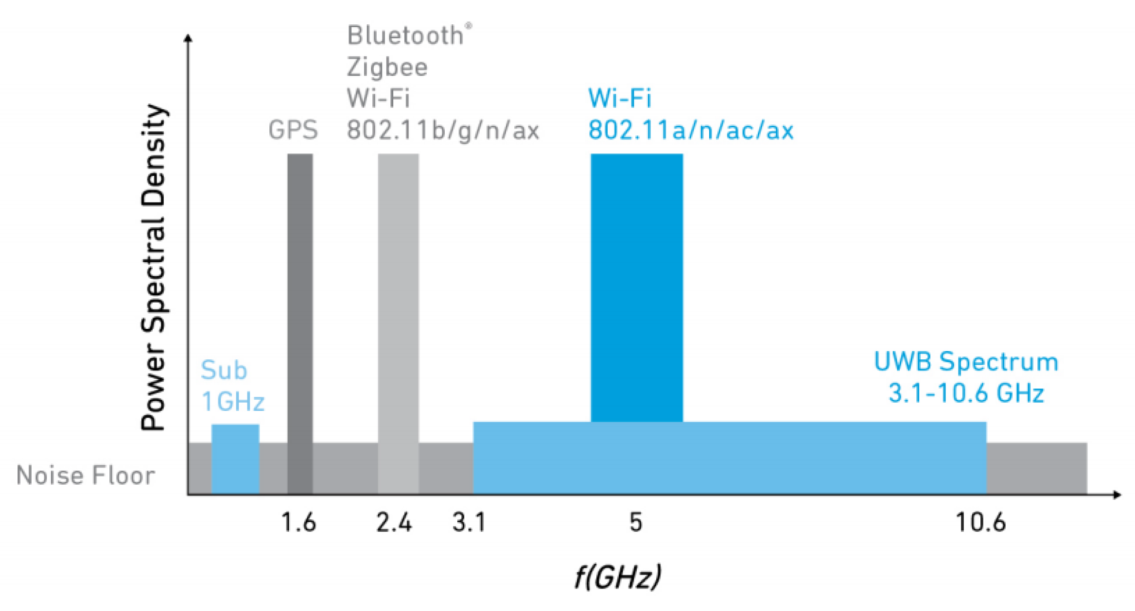
The FCC limits the UWB power to −41.3 dBm to avoid interference with other wireless communication technologies shown in Figure 2 [3,4].
In short, the design of a bandpass filter with an ultra-passband characteristic is a difficult job for microwave researchers compared to other types of BPFs (bandpass filters). For this, continued research has been performed in the design of UWB BPFs using several techniques, such as a complementary split-ring resonator structure [5], a cascaded low and high pass filter topology [6], an interdigital parallel coupled lines [7], a coupled meandered line [8], a composite right/left-handed resonator [9], DGT (defected ground technology) [10], a multimode resonator structure [11,12], a hybrid microstrip, and a coplanar waveguide [13], etc. Recently, a UWB filter was implemented in [14] using tapered transmission line resonators for achieving the fractional bandwidth of 112.2% with wider controllable bandwidth. Initially, the main focus was on the design of a UWB filter with a good fractional bandwidth and out-of-band performance; upto 120% fractional bandwidth was achieved by the authors of [15]. Various types of notched bands at different frequencies were also achieved by the authors using different shaped resonators incorporated into the basic UWB filter design. For example, a single notch has been obtained by utilizing exponentially tapered impedance lines [15], two pairs of tightly coupled λ/2 high-impedance line resonators [16], an asymmetric trisection stepped impedance resonator [17], and an inverted T-shaped resonator in [18]. In [19,20], the authors designed a single-notched UWB filter using quadratic Koch-island and suspended stripline structures. A λ/2 resonator loaded with three short-circuit SIS (step impedance stubs) for the implementation of single notched UWB filter at 5.1 GHz was presented in [21], but the drawback associated with the design is high insertion loss over the entire passband. Recently the authors of [22] used a complex structure for the UWB filter, but the circuit covered a larger area, although the analysis used by the authors is very good for the design of the filter. In [23,24,25], a microstrip to coplanar waveguide transition method was developed for the stopband creation by loading folded split ring resonators to miniaturize the circuit size and spiral resonators on the sectoral defected ground structure, but still, all these have covered a larger circuit area as compared to the structure presented in this work.
This article explores; (1) the parallel coupled microstrip line and multimode resonator structure to design an ultra-passband BPF with a circuit size 0.65 λg × 0.16 λg (where λg is the wavelength corresponding to the central frequency of the UWB filter at 7.2 GHz); (2) a minimal modification to the geometry of the multimode resonator with a coupled rectangular stubs resonator to produce first notch band at 3.5 GHz; and (3) integration of the spur line described by the ABCD parameter analysis to the geometry of the proposed UWB filter to produce another stop band at 7.5 GHz for eliminating the WIMAX and C-band satellite downlink radio signals, respectively. The circuit size for the notched band UWB filter is 0.32 λg × 0.08 λg (where λg is the wavelength corresponding to the central rejection frequency of 3.5 GHz). Moreover, the proposed work is fabricated and tested afterward, and the key attributes have been extracted from the fabricated design which is closely matched with the simulation results. The simulation is performed in a 3D electromagnetic (EM) simulation software Ansys HFSS version-13, while choosing a low-loss PCB [26].
This research work is organized in the following patterns: Section 2 and Section 3 describe the complete analysis of the multimode resonator, spur line structure, and step impedance resonator. Section 4 shows the proposed topology, Section 5 explains how the stopbands are generated, how they will control, and how current distributed over the surface of the filter and finally, Section 6 is the conclusion of this work.

2. Ultra-Wideband Microstrip BPF Design

Calculation and Analysis of the Multimode Resonator Transmission Line
A multimode resonator microstrip line which is also called a step impedance resonator is illustrated in Figure 3a with an equivalent model in Figure 3b, which comprises two identical quarter wavelength high impedance sections with narrow strip width and one central wide strip width half wavelength low impedance transmission line that is energized with two externals 50-ohm parallel coupled microstrip lines for the formation of the UWB range. The parameter Z1, θ1 represents the characteristics impedance and electrical length of the low impedance section, while the parameter Z2, θ2 represents the characteristics impedance and the electrical length of the high impedance section, respectively.
The physical structure of this resonator is identical to the structure discussed in [27]. In the later sections, it will discuss that the proposed structure has the advantage, as it utilizes all the resonance modes for the generation of the passband, whereas in [28], the first resonance mode is utilized for the actual filter design while the other modes generate the spurious harmonics. The input admittance Yin of the proposed multimode resonator can be calculated using the transmission line theory equation
Y i n = j Y 2 2 ( tan θ 1 + tan θ 2 ) ( R tan θ 1 tan θ 2 ) R ( 1 tan 2 θ 1 ) ( 1 tan 2 θ 2 ) 2 ( 1 + R 2 ) tan θ 1 tan θ 2
where R = Z2/Z1 shows the impedance ratio of the proposed resonator, which is responsible for the adjustment of the fundamental resonant modes f1, f2, and f3, respectively. Using the condition Yin = 0 for resonance, the fundamental resonant modes can be extracted from the electrical lengths of both sections (θ1 and θ2) with the condition θ2 = 2θ1 = θ and is calculated using Equations (2)–(6). The following equations are used to determine the physical length and the strip width of the step impedance resonator [29].
θ ( f x ) = tan 1 R R + 2
θ ( f y ) = tan 1 R + 2 R
θ ( f y ) = π 2
f y f x = θ ( f y ) θ ( f x ) = tan 1 R + 2 R tan 1 R R + 2
f z f x = θ ( f z ) θ ( f x ) = π 2 tan 1 R R + 2

3. Dual Stopband Characteristic Analysis

Calculation and Analysis of the Spur Line

A spur line with its equivalent network is shown in Figure 4a,b, which consists of a pair of coupled lines, but connected at one end, and has been studied by the ABCD transmission line method. As shown in Figure 4b, the spur line has two subnetworks; N1, which corresponds to the microstrip line with L = Ls1, W = Ws1, and N2, which corresponds to the transmission line with L = Ls2, W = Ws2, where L and W represent the physical length and width of the microstrip lines with impedances Z3 and Z4, respectively. The termination conditions of the spur line are as follows:
I o = I 1 + I 2 V o = V 1 = V 2 V i = V 1 I i = I i V 2 = 0 , I 2 = 0
After the termination condition is applied to Equation (5) in [30], the four-port network becomes a two-port network. Therefore, the chain matrix is also called the ABCD matrix for the equivalent structure, having characteristic impedances Z3 and Z4 are
N 1 = ( cos θ 1 j Z 3 sin θ 1 j sin θ 1 Z 3 cos θ 1 )
N 2 = ( 1 0 j tan θ 2 Z 4 cos θ 2 1 )
Hence the final chain matrix (ABCD matrix) can be obtained by cascading Equations (8) and (9), respectively.
[ V i I i ] = ( Z 4 cos θ 2 cos θ 1 Z 3 sin θ 1 tan θ 2 j Z 3 sin θ 1 j Z 4 cos θ 2 sin θ 1 + Z 3 cos θ 1 tan θ 2 Z 3 Z 4 cos θ 2 cos θ 1 ) [ V o I o ]
In terms of the ABCD matrix, it can also be written as
[ V i I i ] = ( A B C D ) [ V o I o ]
where the values of A, B, C, and D are;
A = Z 4 cos θ 1 cos θ 2 Z 3 sin θ 1 tan θ 2 Z 4 cos θ 2 B = j Z 3 sin θ 1 C = j Z 4 sin θ 1 cos θ 2 + Z 3 cos θ 1 tan θ 2 Z 3 Z 4 cos θ 2 D = cos θ 1
In the above equations, θ shows the electrical length and is equal to βL (the propagation constant with the physical length L). The transmission coefficient S21 to create the stopband at a specific frequency can be calculated using the equation below [30];
S 21 = 2 A + B / Z o + C Z o + D
The spur line creates a notched band at a specific frequency (S21 = 0 and Zo = 50 Ω) similar to the defective ground structure in [30], which yields the following equation,
cos θ 2 = 0
In [31,32], both the L-shaped spur line and the defective ground structure have the same slow wave features so, the fundamental frequency can be obtained from the method of the defective ground structure and is given below;
f o = 3 × 10 8   m / s 4 L s 2 ε r
The above analysis verifies that the defective microstrip structure (DMS) is suitable for the generation of the stopband in high-frequency applications and mainly depends on the length Ls2 having width Ws2 of the transmission line as shown in Equation (14), i.e., by increasing the resonance frequency, the length Ls2 will decrease. The parametric study of Ls2 can be seen in the result and discussion section. Therefore, the analysis of the spur line discussed in this section is used for the generation of the second notch at 7.5 GHz to suppress the C-band satellite downlink in the UWB range.

Calculation and Analysis of the Rectangular Stub Resonator

The rectangular stub resonator is responsible for the creation of the first notch band at 3.5 GHz for eliminating the WiMAX wireless application and is also called a three-step impedance resonator or low–high–low impedance section, as shown in Figure 5. The length and width of the high and low impedance lines are denoted by La (2θa) with Wa (Z5 = characteristic impedance of high section) and Lb (θb) with Wb (Z6 = characteristic impedance of low section), respectively. The impedance ratio (R) of the half wavelength step impedance resonator, when ignoring the discontinuity, is equal to the ratio of the low to high impedance sections as given below [33];
R = Z6/Z5 = tanθa tanθb
To extend the distance between the first spurious frequency (fs1) and the fundamental resonance frequency (fo), the R should be kept as small as possible and make θa = θb= θo to achieve the resonance condition. Therefore, the mathematical equations of both the resonance condition (θo) and the first spurious frequency (fs1) can be expressed as [34];
θ o = tan 1 R
f s 1 = π f o tan 1 R

4. Proposed Dual-Notch UWB Topology

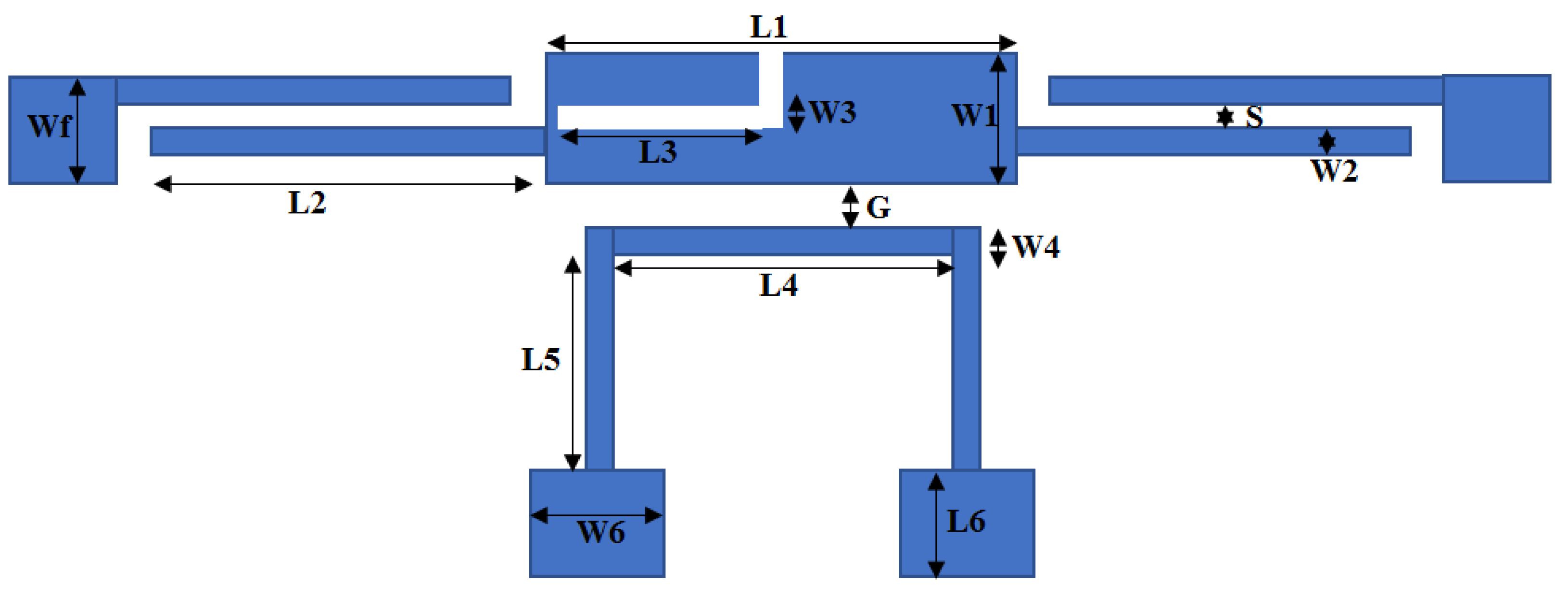
In this study, two filters have been designed and fabricated (1) a UWB filter having size 0.65 λg × 0.16 λg, and (2) a UWB filter with dual notched bands having size 0.32 λg × 0.08 λg have been simulated using a 3D electromagnetic (EM) simulation software Ansys HFSS version-13 and fabricated on Rogers RO-5880 substrate with thickness 0.508 mm, dielectric loss tangent 0.0009, and relative permittivity 2.2, respectively. The device used for measuring the S-parameters was a ZNB-20 vector network analyzer, while the machine used for milling was an LPKF S63 ProtoLaser. The stopband characteristics have been achieved using a rectangular stubs resonator to create the first notch band at 3.5 GHz and spur line structure to get the second stopband at 7.5 GHz for eliminating the WIMAX and C-band satellite downlink radio signals. The proposed topology is shown in Figure 6, along with dimensions in millimeters (mm) listed in Table 1.

5. Experimental Result Discussion of the Proposed UWB BPF with Notched Bands

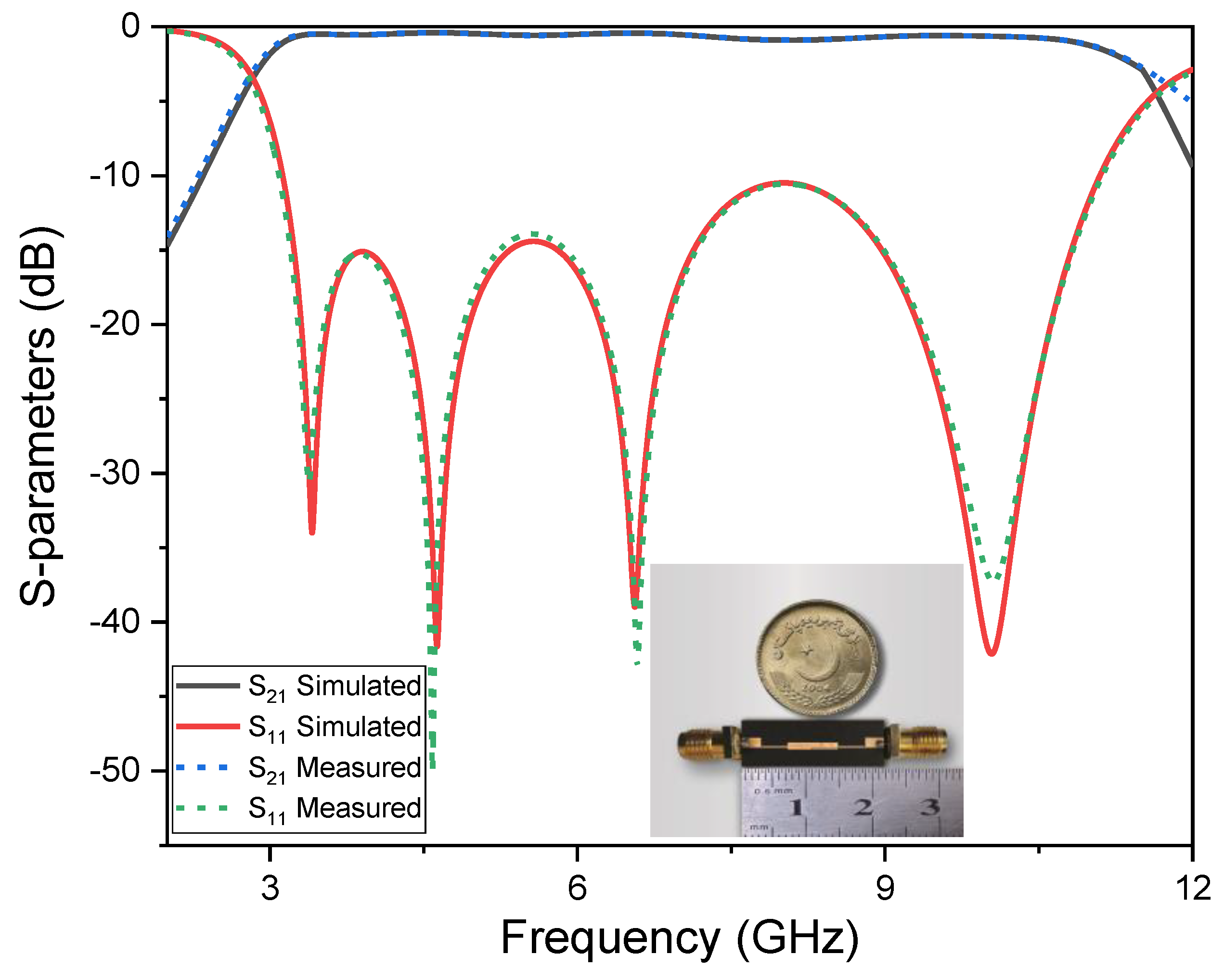
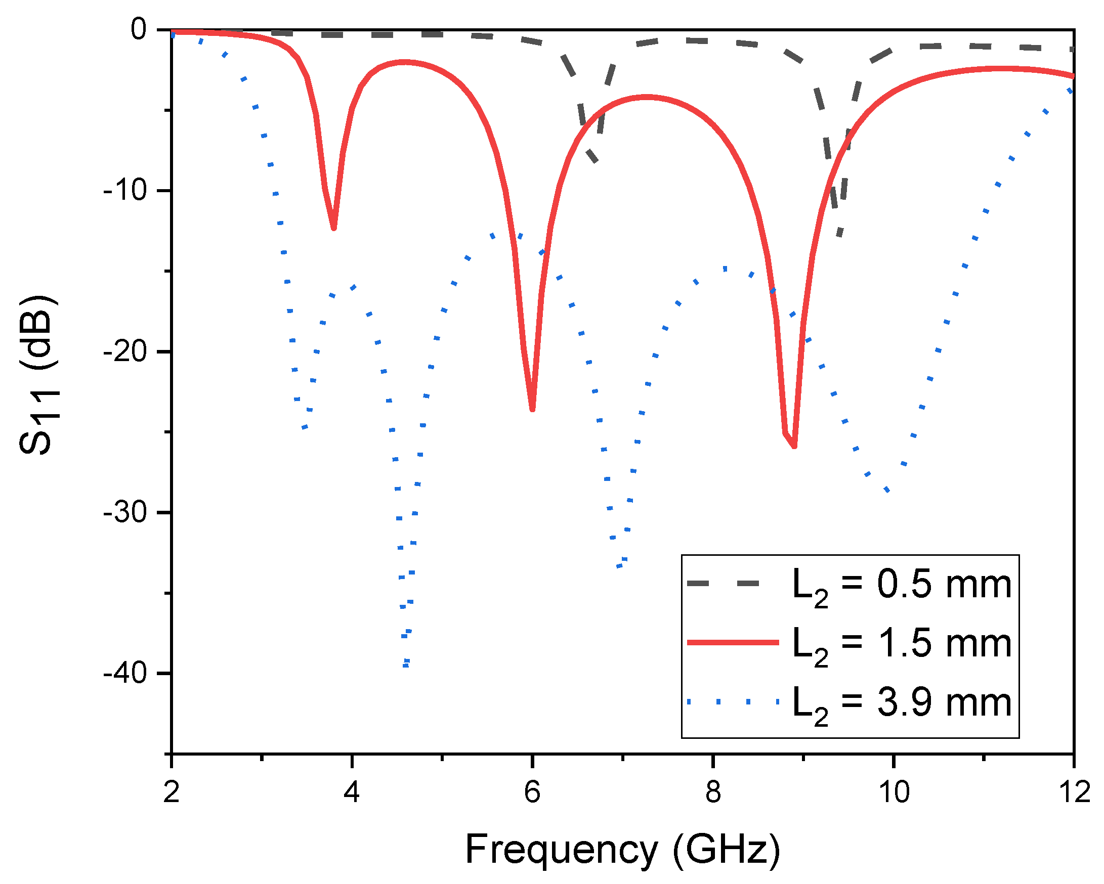
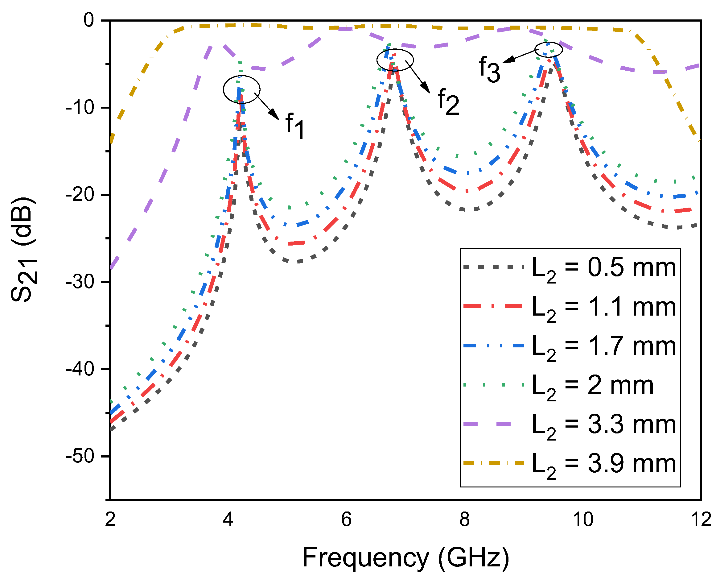
As discussed above, the three resonance modes (f1 = 3.9 GHz, f2 = 7 GHz, and f3 = 9.6 GHz) appeared due to the frequency distributed coupling of the parallel coupled microstrip line of the multimode resonator with space S = 0.05 mm is responsible for the building of the novel multipole UWB BPF design. Figure 7 shows the magnitude of the simulated and measured S11 and S21 plots of the UWB BPF. Under weak coupling (L2 = 0.5 mm) of the parallel coupled microstrip line, only two transmission poles could be observed, but when the coupling gets stronger and stronger by enlarging the length L2, the number of transmission poles also increased within the passband of the UWB BPF, as shown in Figure 8. Now looking at Figure 8 and Figure 9, when the length L2 was enlarged from 0.5 to 1.5 mm, the return loss fell gradually, while the insertion loss rose up and further increased the length L2 to 3.9 mm, which was approximately equal to the λ/4, the S21 shifted to make an ultrawideband BPF with one additional pole and, thus, a total of four transmission poles appeared in the S11 at different frequencies, as shown in Figure 9. In this way, a planar compact ultra-passband filter with an effective circuit area of 0.65 λg × 0.16 λg, fractional bandwidth of 119.4%, insertion loss of −1.1 dB, and S11 > 18dB is implemented in HFSS and fabricated on the low-cost substrate material, respectively.
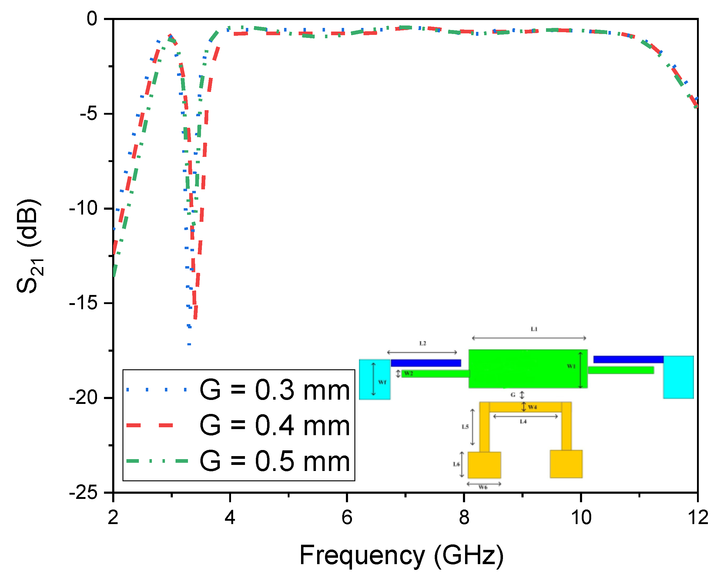
Now, the attention is shifted to how notched bands are formed in the ultrawide passband filter. As discussed above, the two stopbands are formed by the embedded spur line and rectangular stub resonator coupled to the middle section of the proposed multimode resonator structure with the gap G = 0.3 mm. The first notch band for eliminating the frequency at 3.5 GHz was obtained due to the rectangular stubs coupled to the main transmission line, while the second notch band obtained for eliminating the frequency at 7.5 GHz was due to the L-shaped spur line structure, as shown in the Figure 10 and Figure 11, respectively. The first stopband was obtained when the gap between the rectangular stub resonator and the multimode resonator was kept small. Thus, the first stopband appeared when the rectangular stub resonator was strongly coupled to the multimode resonator with a gap G = 0.3 mm. As shown in Figure 10, when the gap increased from 0.3 mm to 0.5 mm, the first stopband peak vanished and went towards −10 dB.
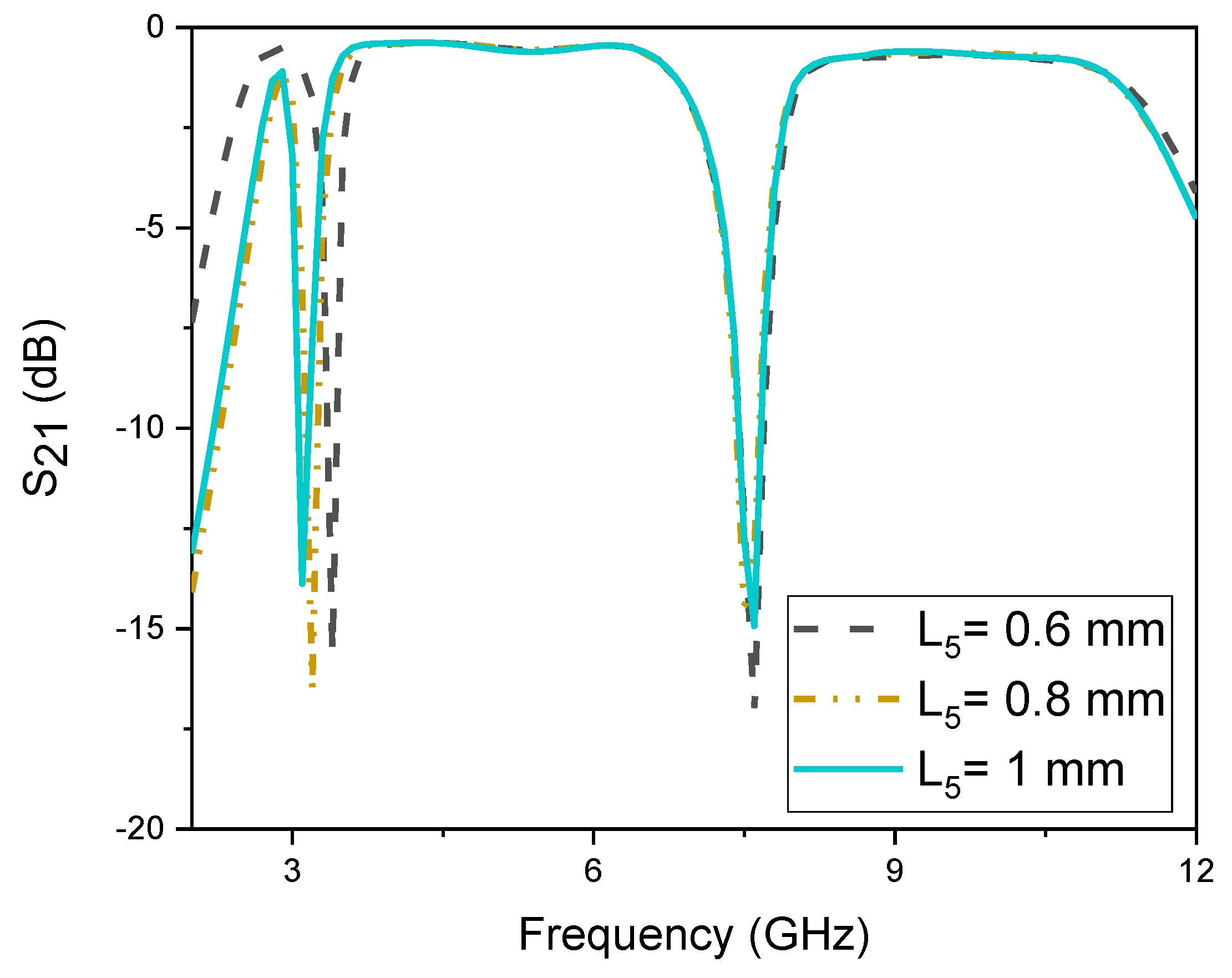
The interesting property of the proposed filter is the independently controlled of both stopbands with the parameters L4, L5, W6, L3, and W3, i.e., by enlarging the parameter L4 from 2 mm to 5 mm, a large variation could be seen in the first stopband, while the second notch band was almost constant, as shown in Figure 12. Similarly, by varying the width W6 and the length L5, a small variation was again obtained, while the second notch band at 7.5 GHz was not changed, as illustrated in Figure 13 and Figure 14, respectively.
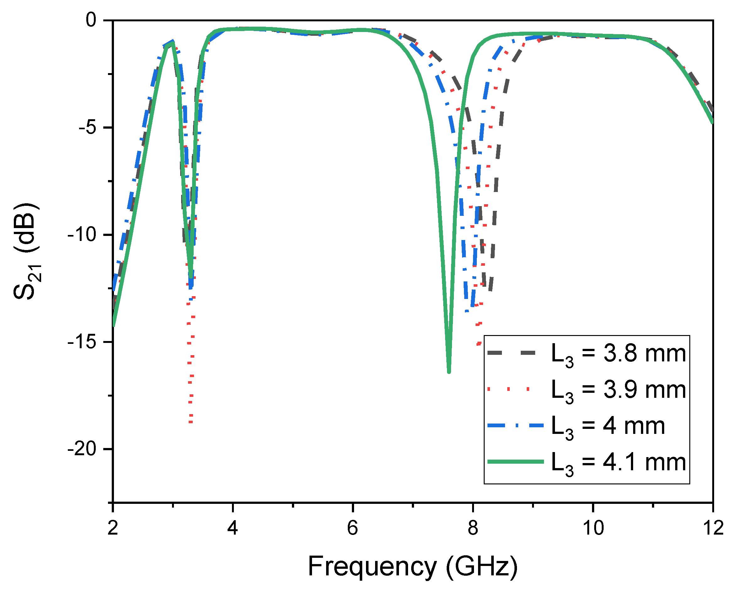
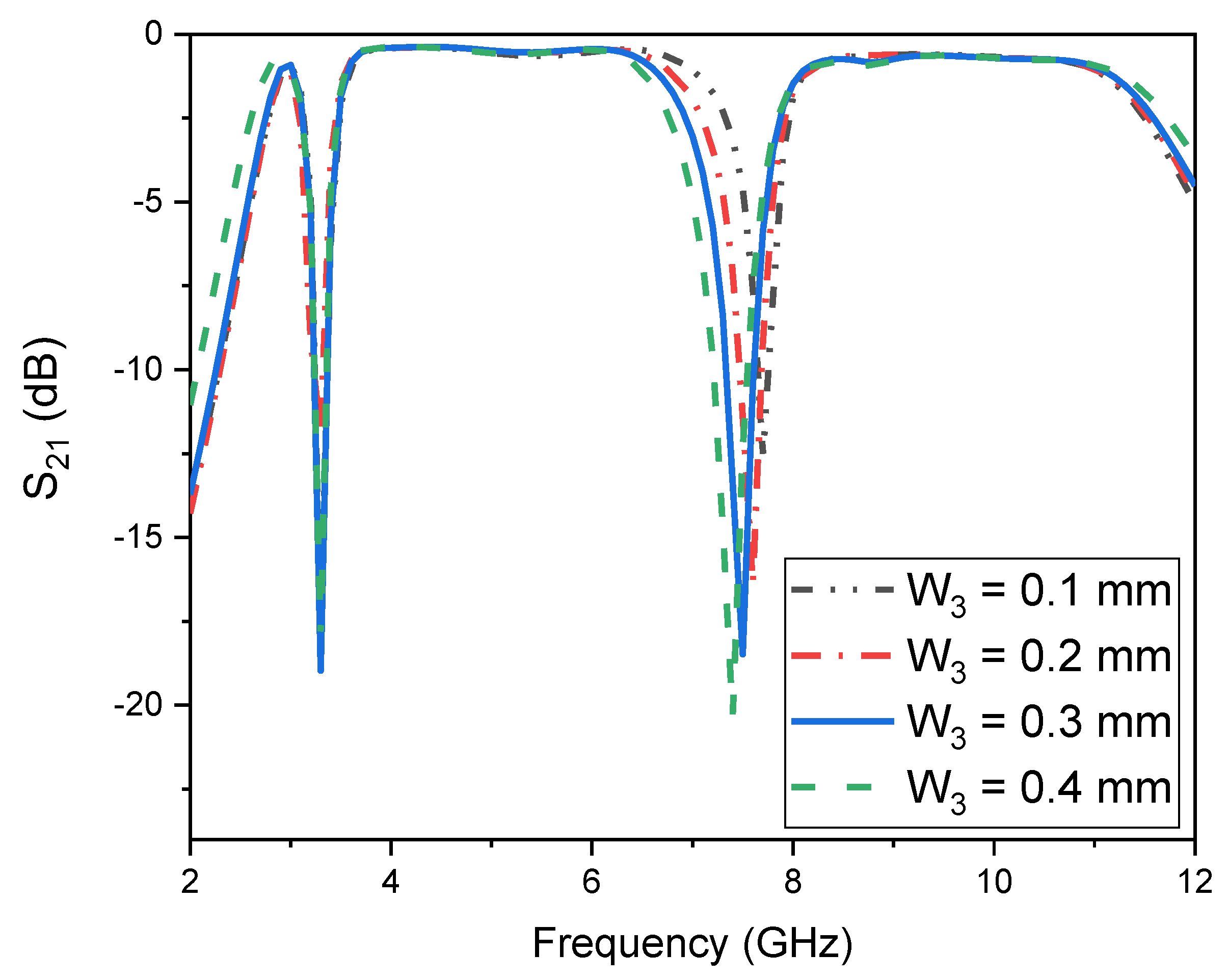
The second notch band at 7.5 GHz is mainly controlled with the parameters L3 and W3, i.e., by small changes in the length L3 from 3.8 mm to 4.1 mm, a large variation can be seen, as shown in Figure 15, while the first stopband was constant. Similarly, when the width W3 increased from 0.1 mm to 0.4 mm, a reasonable change occurred in the second band, while keeping the first stopband constant, as given in Figure 16.
The next important concept that needs to be discussed is the current distribution. It is used to confirm the resonant conditions of the proposed filters. Figure 17 shows the simulated current distributions at the center frequency of the passband response, from 2.8 to 11.5 GHz. As discussed, the strong coupling effect of the parallel coupled lines L2 with narrow space (S) was utilized to excite the ultra-wideband response, as shown in Figure 8 and Figure 9. Therefore, most current energy is absorbed by these lines, thus creating a UWB response. Figure 18 shows the simulated current distributions of the notched filter at a frequency of 3.5 GHz. As discussed above, when the rectangular resonator is coupled with gap G to the multimode resonator, as shown in Figure 10, the first stop band at 3.5 GHz is created. The coupled stub absorbs a relatively high amount of current energy, and this is further verified in Figure 12 by varying the stub L4. Similarly, when the spur line is embedded in the multimode resonator, as shown in Figure 11, the second stopband is achieved at a frequency of 7.5 GHz. The simulated current distributions of the notched filter are observed at this specific frequency near the spur line, as shown in Figure 19. The final graphical record of the current distribution for both notches is shown in Figure 20.
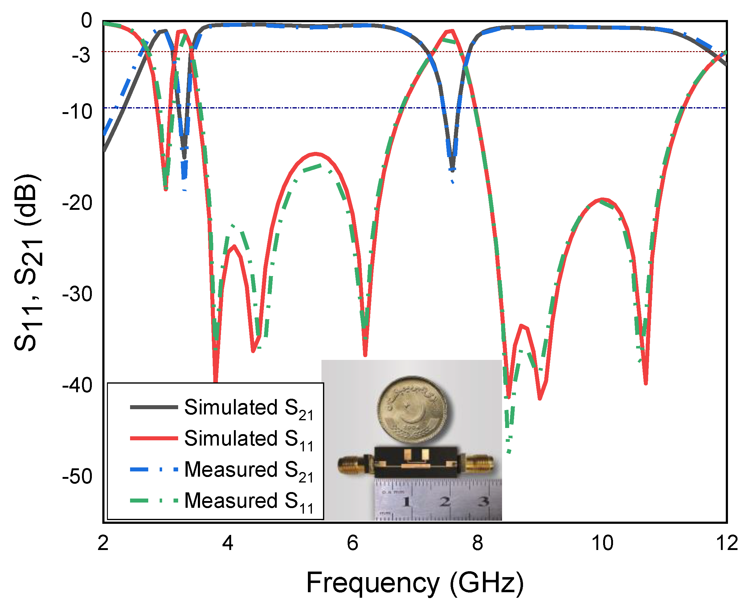
This verifies that the proposed structure eliminates the potential interference in ultra-wideband microwave applications and has the advantage of stopping unwanted wireless bands according to the user’s need. In this research work, the novelty is claimed by using a simple topology to reduce the cost and then compared with the most recent articles published in reputed journals/conferences in terms of its small circuit size, good FBW, low insertion loss over the entire UWB range, high returns loss, and independently controlled notch bands which are tabulated in Table 2, respectively. Moreover, the final S11 and S21 frequency plots of the proposed dual notch UWB BPF, with a fabricated photograph, are shown in Figure 21.

6. Conclusions

This article presented a new compact multipoles UWB BPF with adjustable dual stopband frequencies using extremely high coupled parallel microstrip lines with embedded spur line structure and rectangular stub resonator to suppress the unwanted frequency signals at 3.5 GHz for WiMAX with an absolute bandwidth of 310 MHz and 7.5 GHz with an absolute bandwidth 690 MHz for C-band satellite downlink communication system, respectively. The filter has some attractive features such as compact size, good reflection coefficient lower than −18 dB, good insertion loss of −1.1 dB over the entire passband, and multiple transmission poles, which made the proposed filter much better than those discussed in the literature. Finally, the filter has been measured and tested, and the results obtained were in good agreement.

Author Contributions

Conceptualization, A.B. and G.Z.; methodology, A.B.; software, A.B., N.S., M.I.K. and A.D.; formal analysis, A.D.; investigation, A.B.; resources, A.D.; data curation, A.B.; writing—original draft preparation, A.B.; writing—review and editing, G.Z.; visualization, A.B. and A.D.; supervision, G.Z.; project administration, G.Z.; funding acquisition, G.Z. All authors have read and agreed to the published version of the manuscript.

Funding

This work is supported by “Young Talent Sub-project of Ningbo Yongjiang Talent Introduction Programme under grant no 20100859001.”

Data Availability Statement

Not applicable.

Conflicts of Interest

The authors declare no conflict of interest.

References

  1. Wang, L.T.; Xiong, Y.; He, M.; Kheir, M. Review on UWB bandpass filters. In UWB Technology-Circuits and Systems; IntechOpen: London, UK, 2019; pp. 1–24. [Google Scholar]
  2. FCC. Revision of Part 15 of the Commission’s Rules Regarding Ultra-Wideband Transmission System; FCC: Washington, DC, USA, 2002. [Google Scholar]
  3. Khattak, M.I.; Khan, M.I.; Anab, M.; Ullah, A.; Al-Hasan, M.; Nebhen, J. Miniaturized CPW-fed UWB-MIMO antennas with decoupling stub and enhanced isolation. Int. J. Microw. Wirel. Technol. 2022, 14, 456–464. [Google Scholar] [CrossRef]
  4. Basit, A.; Khattak, M.I.; Zubir, F.; Shah, S.W. Miniaturized ultra-wideband filter with independently controlled notch bands for 5.1/6/8 GHz wireless applications. PloS ONE 2022, 17, e0268886. [Google Scholar] [CrossRef] [PubMed]
  5. Sarkar, D.; Moyra, T.; Murmu, L. An ultra-wideband (UWB) bandpass filter with complementary split ring resonator for coupling improvement. Int. J. Electron. Commun. 2017, 71, 89–95. [Google Scholar] [CrossRef]
  6. Gomez-Garcia, R.; Alonso, J.I. Systematic method for the exact synthesis of ultra-wideband filtering responses using high-pass and low-pass sections. IEEE Trans Microw Theory Tech. 2006, 54, 3751–3764. [Google Scholar] [CrossRef]
  7. Xia, X.; Chen, F.; Cheng, X.; Deng, X. A compact ultra-wideband bandpass filter with good selectivity based on interdigital coupled-line. Int. J. RF Microw. Comput. -Aided Eng. 2018, 28, e21419. [Google Scholar] [CrossRef]
  8. Jiang, Y.; Tang, W.; Shi, Y.; Zhou, P.; Feng, L. Compact and low insertion loss UWB on-chip bandpass filter using coupled meandered line. Microw. Opt. Technol. Lett. 2020, 62, 2236–2242. [Google Scholar] [CrossRef]
  9. Li, C.; Tong, C.; Qi, L.; Zou, X.; Ji, M. Multimode resonator based on composite right-/left-handed transmission line for UWB bandpass filter application. Int. J. RF Microw. Comput. -Aided Eng. 2015, 25, 815–824. [Google Scholar] [CrossRef]
  10. Sahu, B.; Singh, S.; Meshram, M.K.; Singh, S.P. Super-compact ultra-wideband microstrip band-pass filter with improved performance using defected ground structure-based low-pass filter. J. ElEctromagnEtic WavEs Appl. 2018, 32, 635–650. [Google Scholar] [CrossRef]
  11. Kumar, S.; Gupta, R.D.; Parihar, M.S. Multiple band notched filter using C-shaped and E-shaped resonator for UWB applications. IEEE Microw. Wirel. Compon. Lett. 2016, 26, 340–342. [Google Scholar] [CrossRef]
  12. Shome, P.P.; Khan, T. A compact design of circular-ring shaped MMR based bandpass filter for UWB applications. In Proceedings of the 2019 IEEE Asia-Pacific Microwave Conference (APMC), Singapore, 13 December 2019. [Google Scholar]
  13. Kuo, T.N.; Lin, S.C.; Chen, C.H. Compact ultra-wideband bandpass filter using composite microstrip-coplanar-waveguide structure. IEEE Trans. Microw. Theory Tech. 2006, 54, 3772–3778. [Google Scholar] [CrossRef]
  14. Razzaz, F.; Saeed, S.M.; Alkanhal, M.A. Ultra-Wideband Bandpass Filters Using Tapered Resonators. Appl. Sci. 2022, 12, 3699. [Google Scholar] [CrossRef]
  15. Sangam, R.S.; Kshetrimayum, R.S. Notched UWB filter using exponential tapered impedance line stub loaded microstrip resonator. J. Eng. 2018, 2018, 768–772. [Google Scholar] [CrossRef]
  16. Weng, M.H.; Hsu, C.W.; Lan, S.W.; Yang, R.Y. An ultra-wideband bandpass filter with a notch band and wide upper bandstop performances. Electronics 2019, 8, 1316. [Google Scholar] [CrossRef] [Green Version]
  17. Kumari, P.; Sarkar, P.; Ghatak, R. A multi-stub loaded compact UWB BPF with a broad notch band and extended stopband characteristics. Int. J. RF Microw. Comput. Aided Eng. 2020, 30, e22138. [Google Scholar] [CrossRef]
  18. Ranjan, P.; Kishore, N.; Dwivedi, V.K.; Upadhyay, G.; Tripathi, V.S. UWB filter with controllable notch band and higher stop band transmission zero using open stub in inverted T-shaped resonator. In Proceedings of the 2017 IEEE Asia Pacific Microwave Conference (APMC), Kuala Lumpur, Malaysia, 13 November 2017; pp. 817–820. [Google Scholar]
  19. Bhaskar, M.; Mathew, T. Ultra-wideband bandpass filter with notch band based on quadratic Koch island structure. Indones. J. Electr. Eng. Inform. 2021, 9, 793–798. [Google Scholar] [CrossRef]
  20. Xu, Z. UWB bandpass SSL filter with an adjustable notched band and four transmission zeros. Electron. Lett. 2021, 57, 930–932. [Google Scholar] [CrossRef]
  21. Liu, L.Q.; Lai, H.S.; Hu, H.M.; Chen, J.J.; Weng, M.H.; Yang, R.Y. A Simple Method to Design a UWB Filter with a Notched Band Using Short-Circuit Step Impedance Stubs. Electronics 2022, 11, 1124. [Google Scholar] [CrossRef]
  22. Bandyopadhyay, A.; Sarkar, P.; Ghatak, R. A Bandwidth Reconfigurable Bandpass Filter for Ultrawideband and Wideband Applications. IEEE Trans. Circuits Syst. II Express Briefs 2022, 69, 2747–2751. [Google Scholar] [CrossRef]
  23. Ghazali, A.N.; Sazid, M.; Pal, S. A miniaturized low-cost microstrip-to-coplanar waveguide transition-based ultra-wideband bandpass filter with multiple transmission zeros. Microw. Opt. Technol. Lett. 2020, 62, 3662–3667. [Google Scholar] [CrossRef]
  24. Ghazali, A.N.; Sazid, M.; Pal, S. Multiple passband transmission zeros embedded compact UWB filter based on microstrip/CPW transition. Int. J. Electron. Commun. 2021, 129, 1–6. [Google Scholar] [CrossRef]
  25. Ghazali, A.N.; Sazid, M.; Pal, S. A dual notched band UWB-BPF based on microstrip-to-short circuited CPW transition. Int. J. Microw. Wirel. Technol. 2018, 10, 794–800. [Google Scholar] [CrossRef]
  26. Ansoft Corporation. Ansoft HFSS, version 13. Available online: https://www.ansys.com/products/electronics/ansys-hfss (accessed on 17 December 2022).
  27. Hsieh, L.H.; Chang, K. Compact, low insertion-loss, sharp-rejection, and wide-band microstrip bandpass filters. IEEE Trans. Microw.Theory Tech. 2003, 51, 1241–1246. [Google Scholar] [CrossRef]
  28. Makimoto, M.; Yamashita, S. Bandpass filters using parallel coupled stripline stepped impedance resonators. IEEE Trans. Microw. Theory Tech. 1980, 28, 1413–1417. [Google Scholar] [CrossRef]
  29. Gupta, K.C.; Garg, R.; Bahl, I.; Bhartia, P. Microstrip Lines and Slotlines, 2nd ed.; Artech House: Norwood, MA, USA, 1996. [Google Scholar]
  30. Bates, R.N. Design of microstrip spur-line band-stop filters. IEEE J. Microw. Opt. Acoust. 1977, 1, 209–214. [Google Scholar] [CrossRef]
  31. Wang, J.; Ning, H.; Xiong, Q.; Li, M.; Mao, L.F. A novel miniaturized dual-band bandstop filter using dual-plane defected structures. Prog. Electromagn. Res. 2013, 134, 397–417. [Google Scholar] [CrossRef] [Green Version]
  32. Hong, J.S.; Karyamapudi, B.M. A general circuit model for defected ground structures in planar transmission lines. IEEE Microw. Wirel. Compon. Lett. 2015, 15, 706–708. [Google Scholar] [CrossRef]
  33. Basit, A.; Khattak, M.I.; Althuwayb, A.; Nebhen, J. Compact Tri-band Bandpass Filter Based on Asymmetric Step Impedance Resonators for WiMAX and RFID Systems. J. Electromagn. Eng. Sci. 2021, 21, 316–321. [Google Scholar] [CrossRef]
  34. Basit, A.; Khattak, M.I.; Nebhen, J.; Jan, A.; Ahmad, G. Investigation of external quality factor and coupling coefficient for a novel SIR based microstrip tri-band bandpass filter. PLoS ONE 2021, 16, e0258386. [Google Scholar] [CrossRef]
  35. Sazid, M.; Raghava, N.S. Planar UWB-bandpass filter with multiple passband transmission zeros. Int. J. Electron. Commun. 2021, 134, 1–7. [Google Scholar] [CrossRef]
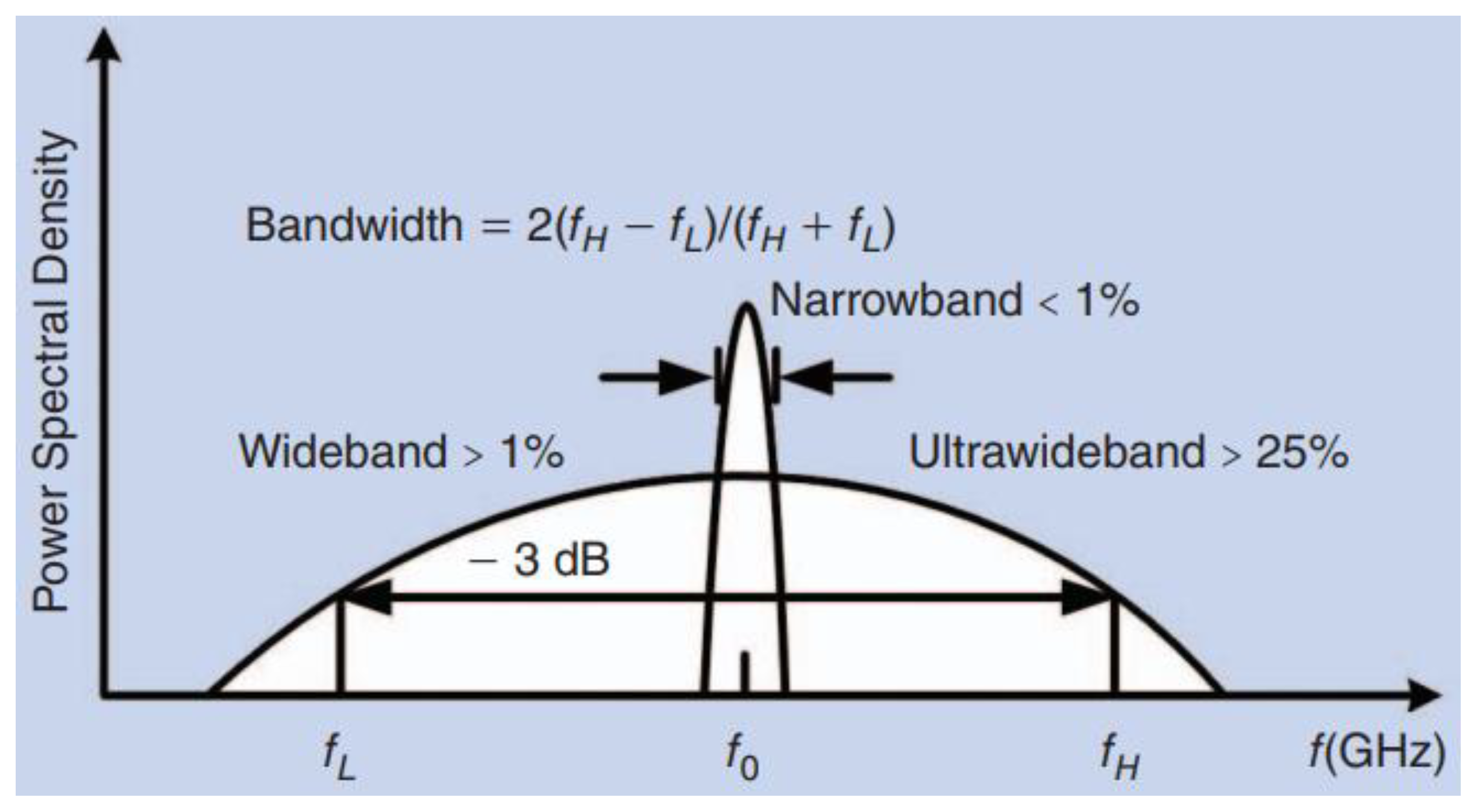
Figure 1. fL, fo, fH frequencies of UWB spectrum [1].
Fractalfract 07 00112 g001
Figure 2. UWB interference with other wireless communication bands [1].
Fractalfract 07 00112 g002
Figure 3. (a) Multimode resonator with step impedance configuration. (b) Equivalent configuration of the multimode resonator.
Fractalfract 07 00112 g003
Figure 4. (a) Proposed spur line configuration. (b) Equivalent configuration of the spur line.
Fractalfract 07 00112 g004
Figure 5. Proposed rectangular stub configuration.
Fractalfract 07 00112 g005
Figure 6. Schematic diagram of the dual-notched UWB BPF.
Fractalfract 07 00112 g006
Figure 7. Simulated and measured S11 and S21 frequency plots of the initial UWB BPF.
Fractalfract 07 00112 g007
Figure 8. Transmission poles appearance w.r.t parameter L2.
Fractalfract 07 00112 g008
Figure 9. The magnitude of |S21| under different coupling scheme w.r.t parameter L2.
Fractalfract 07 00112 g009
Figure 10. S21 plot of UWB notch filter with proposed rectangular stubs.
Fractalfract 07 00112 g010
Figure 11. S21 plot of UWB notch filter with embedded spur line structure.
Fractalfract 07 00112 g011
Figure 12. S21 plot of first band control with parameter L4.
Fractalfract 07 00112 g012
Figure 13. S21 plot of first band control with parameter W6.
Fractalfract 07 00112 g013
Figure 14. S21 plot of first band control with parameter L5.
Fractalfract 07 00112 g014
Figure 15. S21 plot of second band control with parameter L3.
Fractalfract 07 00112 g015
Figure 16. S21 plot of second band control with parameter W3.
Fractalfract 07 00112 g016
Figure 17. Current distribution of the UWB filter at central frequency 7.2 GHz.
Fractalfract 07 00112 g017
Figure 18. Current distribution of the UWB filter with a notch at 3.5 GHz.
Fractalfract 07 00112 g018
Figure 19. Current distribution of the UWB filter with a notch at 7.5 GHz.
Fractalfract 07 00112 g019
Figure 20. Current distribution of the UWB filter with dual notched band characteristics.
Fractalfract 07 00112 g020
Figure 21. EM-simulated and measured frequency plots responses of the proposed dual-notched UWB-BPF.
Fractalfract 07 00112 g021
Table 1. Proposed filter dimensions in mm.
L21W5.2L17.52W11.08
L24.13W20.1L34.15W30.1
L45W40.25L50.75L62.8
W61.8Wf1.48S0.05G0.3
Table 2. Comparison with other reported work.
Ref.Passband (GHz)FBW (%)S11, S21 (dB)No. of NotchesCircuit Size
g × λg)
[16]3.4–1098.522.7, 0.711.09 × 0.44
[17]2.86–10.72115.7>40, <110.67 × 0.46
[19]3.38–9.79621.2, 0.3911.02 × 1.08
[20]2.9–10.611419, <1.310.73 × 0.34
[22]2.15–11.18129.5>10, 1.510.80 × 0.42
[23]2.75–10.711815.5, <0.87–<1.821.01 × 0.76
[24]2.9–10.511315.5, 121.01 × 0.76
[25]3–10.9113.6>15, 0.620.90 × 0.51
[35]
Filter1
3.25–10.73
2.9–11.5
106
119.4
17.3, 0.8
>10, <1.1
2
No
1.34 × 0.41
0.65 × 0.16
Filter22.9–11.5119.4>18, <1.120.32 × 0.08
FBW = fractional bandwidth, S21 = insertion loss, S11 = return loss λg = 7.2 GHz for filter 1 and 3.5 GHz for filter 2.
Disclaimer/Publisher’s Note: The statements, opinions and data contained in all publications are solely those of the individual author(s) and contributor(s) and not of MDPI and/or the editor(s). MDPI and/or the editor(s) disclaim responsibility for any injury to people or property resulting from any ideas, methods, instructions or products referred to in the content.