1. Introduction
Penetration of molecular/cluster ions through a solid is characterized by simultaneous collisions of many ions with target atoms in a small space. This can result in highly dense energy deposition; for example, C
60-ion bombardment can induce highly dense electronic excitation or dense collision cascades, which monatomic–ion bombardment can never induce. One of the most important effects resulting from such a highly dense energy deposition is the strong sputtering localized around the surface layer, which is different from the case by monatomic ions. In these decades, intensive application studies of the sputtering by C
60 ions have been made based on this effect for possible applications to the surface-sensitive analyses and secondary-ion-mass spectroscopy (SIMS), especially of high-polymer materials and/or biomaterials [
1]. The progress of such application studies has also expanded a basic understanding of the unique sputtering phenomenon induced by C
60-ion bombardment [
2]. In parallel with such experimental studies, computer simulation studies have provided a non-empirical, essential insight into the phenomenon [
3]. However, supporting data consistent with the results from the simulations have still not been obtained enough: for example, energy dependence of the sputtering yield and of the deposition, or implantation of carbon atoms, and the depth of a surface layer affected by the bombardment.
The linear-collision-cascade theory of Sigmund well describes the energy dependence of the sputtering yield of a polycrystalline or amorphous single-element solid bombarded with monatomic ions [
4]. When the atomic numbers of the projectile and the target are large, however, the deviation of experimental sputtering yields from the theoretical predictions is found: It is called a nonlinear effect. Especially, the effect is more significant in the case of molecular/cluster-ion bombardment [
5]. Andersen and the Orsay group have reported that the Au sputtering yield by Au
n-ion (
n ≤ 13) bombardment is proportional to
n2 in the energy range, where the nuclear stopping is dominant [
6,
7]. This nonlinear effect can be explained by an elastic-collision thermal-spike model [
8]. In the case of the C
60-ion bombardment, the similar nonlinear effect can be expected because of quite a large
n. Compared with the above Au case, however, the atomic number of the projectile is rather low; thus, it is interesting to investigate how the nonlinear effect is in the case of the C
60 ion, because the effect has not been observed for projectiles of low atomic numbers.
In this study, we present sputtering yield measurements of Si targets bombarded with C
60 ions in the energy range from 10 to 540 keV, where the nuclear stopping is dominant. To the best of our knowledge, they are the first comprehensive sputtering-yield data by C
60-ion bombardment. The obtained result will be compared with sputtering yields for a carbon monatomic ion calculated using Sigmund’s theory and the SRIM2008 code [
9], and the nonlinear effect will be discussed.
2. Materials and Methods
Small pieces of Si(100) wafer (Nilaco Co., Tokyo, Japan), 5 × 13 mm
2, which was the n-type and whose resistivity was less than 0.02 Ωcm, were cleaned with the RCA method [
10] to reduce carbon contaminants and to remove a native oxide layer on the surface prior to irradiation. The pieces were irradiated with 200-keV Ar
+ ions at the fluence of 5 × 10
15 ions/cm
2 to make an amorphous Si layer of approximately ~360 nm at the surface at first; then, they were irradiated with 10–120-keV C
60+ or 100–540-keV C
602+ ions. The angle of the C
60-ion beam to the Si surface was 90°. Commercial Al foil with the thickness of 11 μm, which was folded double, was used for masking. Both Ar- and C
60-ion irradiations were performed at room temperature using the 400-kV ion implanter (NH-40SR, Nissin Electrics Co., Kyoto, Japan) of the Cockcroft–Walton type of TIARA, QST/Takasaki [
11]. Two-thirds of a target piece was irradiated with Ar
+ ions, and a half of the Ar-irradiated area was irradiated with C
60 ions; thus, one target piece has three areas, i.e., unirradiated, Ar-irradiated, and Ar- and C
60-irradiated. After the C
60-ion irradiation, the change in the thickness of an amorphous layer was measured with a conventional Rutherford-backscattering spectroscopy (RBS) using 2-MeV He
+ ions by the 3-MV single-ended accelerator of TIARA. The projected range of 540-keV C
60 ions in Si is 31 nm, which was the maximum one in this study and was estimated with the SRIM2008 code; in addition, the thickness of an amorphous layer after C
60-ion irradiation was approximately 210 nm at least in this study; thus, it was thick enough to stop the projectiles within the amorphous layer, whatever their energy.
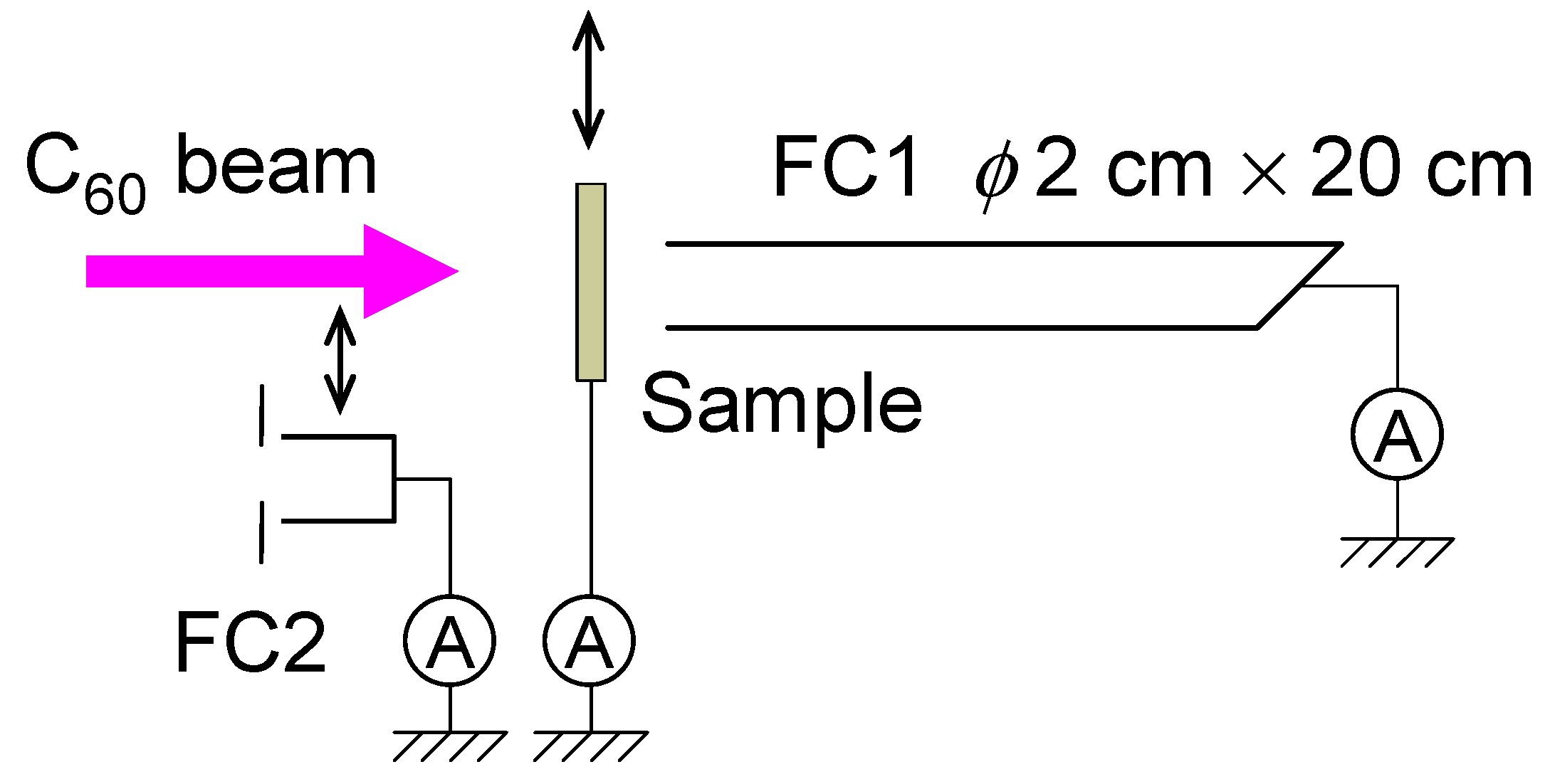
The details of the C
60-irradiation are as follows. The schematic drawing of the experimental setup is shown in
Figure 1. C
60 powder was vaporized in an oven and fed into a plasma chamber to produce C
60 ions in a Freeman-type ion source of the ion implanter [
12]. Positive ions generated in the ion source were extracted and were mass-analyzed using a mass-analyzing magnet in a high voltage terminal to produce C
60 ions of a desired charge state. A C
60-ion beam, whose spot size was typically several mm in diameter, was swept vertically and horizontally using two sets of parallel-plate deflectors and irradiated on a target through both a 4-blade slit and a square aperture of 5 × 5 mm
2. The irradiated area was evaluated from the sputtered area by irradiation of a thin copper-oxide film with a C
60-ion beam, which had been prepared by thermal oxidation on a thin Cu plate; the typical area was approximately 8 × 8 mm
2. The beam current was measured with a removable Faraday cup 2 (FC2) connected to a digital electrometer (Advantest R8240) shown in
Figure 1 immediately before and after the irradiation. The measured current was calibrated with a Faraday cup 1 (FC1), which is able to measure the correct cluster-ion-beam current, because of a very small solid angle of its entrance that is able to eliminate the influence of the secondary-charged-particle emission. The typical beam current was a few to a few 10′s nA. In order to monitor the fluctuation in the beam current, the apparent target current was recorded during C
60-ion irradiation. The C
60-ion fluence was estimated from the average of the measured beam currents and the irradiation time. The fluence of the C
60 ion was 1 × 10
14 to 1 × 10
15 C
60/cm
2.
3. Results
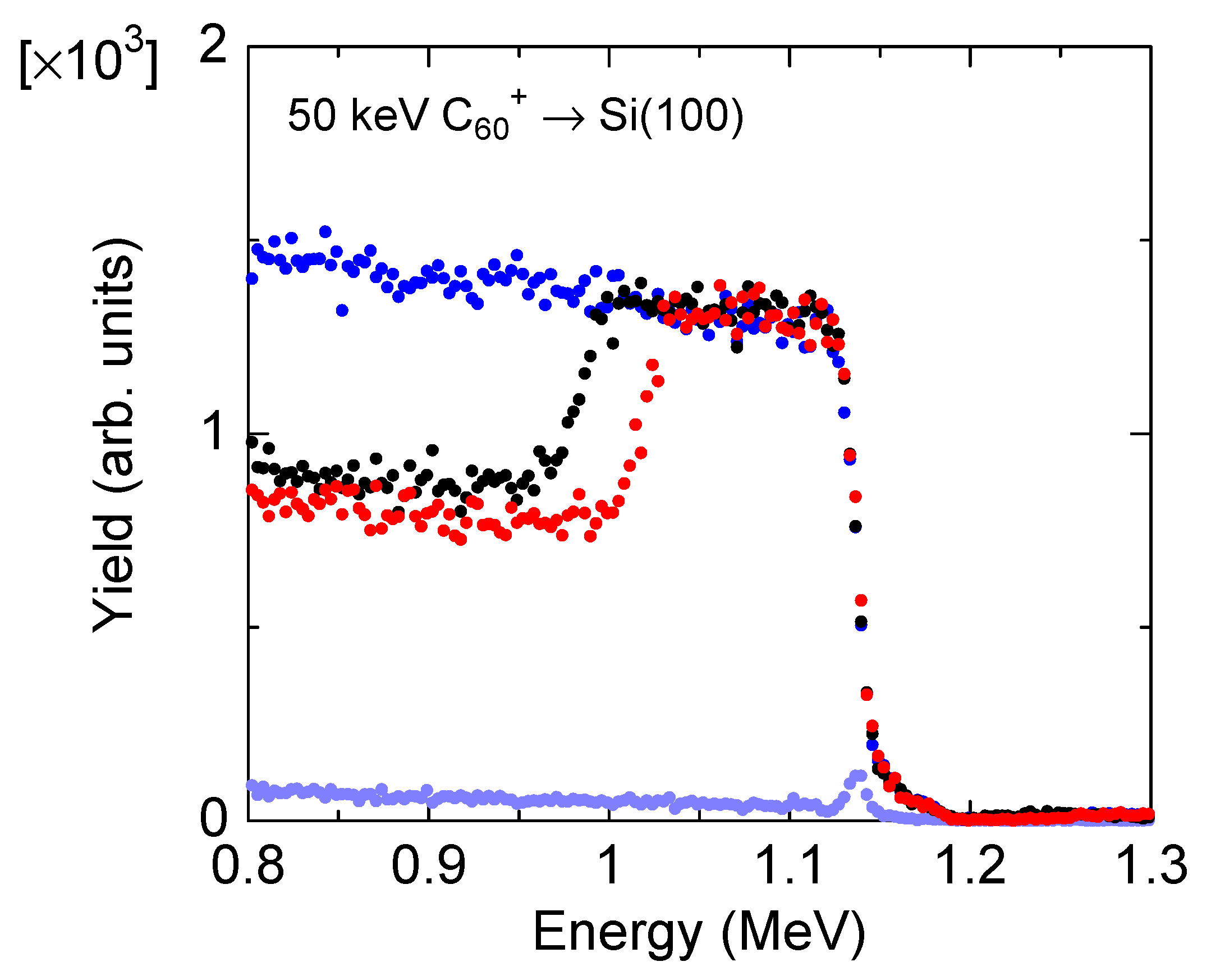
Figure 2 shows examples of RBS spectra for a Si sample irradiated with 50-keV C
60+ ions at the fluence of 7.3 × 10
14 C
60/cm
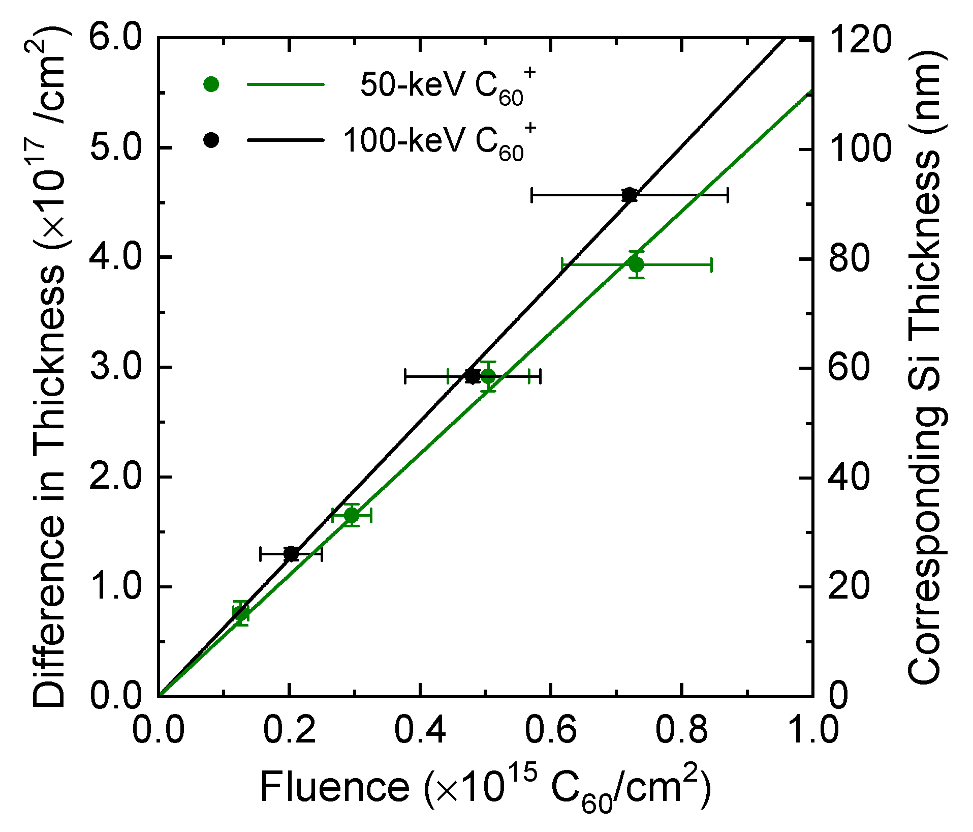
2: three spectra for three different areas on the same sample under the <100>-axial channeling condition and a spectrum under the random condition. Under the axial channeling condition, the scattering yield from the amorphous layer coincides with that under the random condition, and there is a decrease in the scattering yield at the interface between the amorphous layer and the single-crystal substrate. Therefore, the energy interval over which the scattering yield reaches the random yield corresponds to the thickness of the amorphous layer. The thickness change of an amorphous layer was determined by spectra measured under the <100>-axial channeling condition. The obtained thickness change of an amorphous layer after C
60-ion irradiation was plotted as a function of C
60-ion fluence: the typical examples are shown in
Figure 3. The main contribution to the uncertainties of C
60-ion fluence is that of the irradiated area. The solid lines in the figure are obtained from the least-squares method. It is obviously shown that the difference in thickness is proportional to the C
60-ion fluence. Thus, the Si sputtering yield was derived from the slope of the line. For energies where only one value of the thickness change was obtained, the sputtering yield was derived from the ratio of the thickness change to the C
60-ion fluence.
Obtained sputtering yields of Si bombarded with C
60 ions are shown in
Figure 4 as a function of the energy per atom as well as of the energy of a C
60 ion. As obviously shown, the sputtering yield steeply increases with the energy at lower energies and has the maximum, approximately 600 Si/C
60, around 100 keV: The maximum is approximately twenty times as large as the one at 10 keV. At higher energies than 120 keV, the sputtering yield decreases. It should be noted that the obtained sputtering yield is hardly dependent on the charge state of a projectile C
60 ion.
4. Discussion
In order to evaluate the measured sputtering yields, they were compared with those by bombardment with a C monatomic ion with the same velocity. Because the corresponding experimental Si sputtering yields for C monatomic ions are not available, the Si sputtering yield for a monatomic ion was calculated both based on the linear-collision-cascade theory of Sigmund [
4] and using the SRIM2008 code [
9]. According to Sigmund’s theory, sputtering yield
Y1 for backward sputtering at a perpendicular incidence is given by,
where
α(
M2/
M1) is an energy-independent function of the mass ratio, 0.456 for
M2/
M1 = 2.33,
Sn a nuclear stopping power,
N the number density of target atoms, 4.9770 × 10
22 atoms/cm
3 for Si,
U0 the sublimation energy of a target, 4.63 eV for Si.
M1 and
M2,
Z1 and
Z2, and
E are the mass numbers of the projectile and the target, the atomic numbers of the projectile and the target, and the energy of the projectile, respectively. In the calculation, the nuclear stopping power for a C monatomic ion was calculated using the SRIM2008 code. The calculated result is shown by the solid line in
Figure 4. In
Figure 4, the lower and upper abscissas denote the energy of C
60 ions and the energy per atom of the projectiles, respectively, and both are scaled so that the energy per atom can be expressed at the same position in both; so are the ordinates: the sputtering yield per atom,
Yn/
n can be expressed at the same position in both. Si sputtering yields for C monatomic ions calculated with the simulation using the SRIM2008 code are denoted by the diamonds in
Figure 4. The conditions of the simulation are as follows: The lattice binding energy, the surface binding energy and the displacement energy are 2.0 eV, 4.63 eV and 15.8 eV, respectively. Both results are almost the same: Both have the same maximum sputtering yield around 3–4 keV/atom, where the nuclear stopping power has the maximum; however, the sputtering yields by Sigmund’s theory are slightly larger except around the maximum. The measured sputtering yields per atom
Y60/60 are larger than those both by Sigmund’s theory and by the SRIM2008 code except for 10-keV C
60 ions, which indicates that the nonlinear effect on the sputtering yield has been observed.
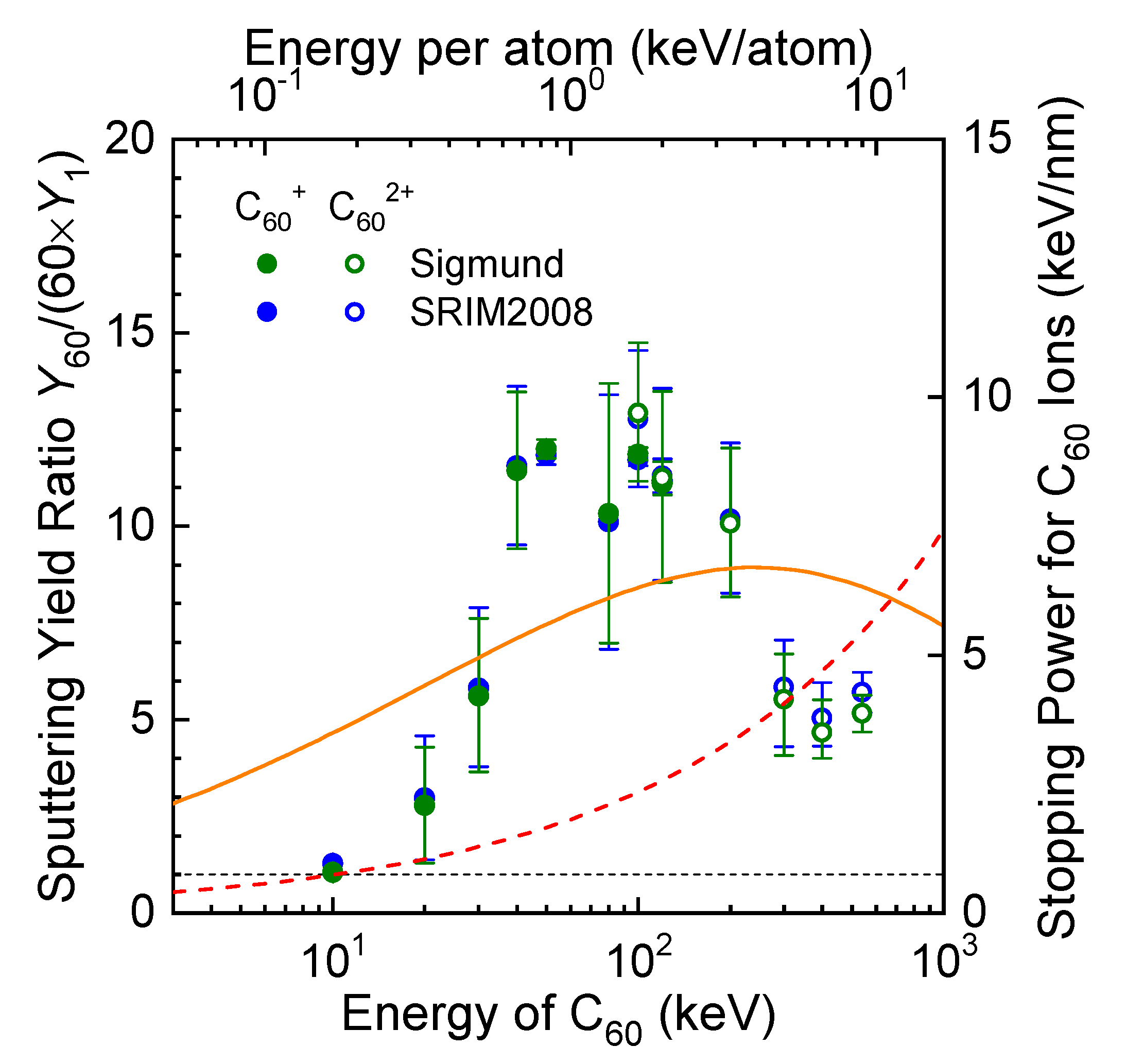
Let us introduce the sputtering-yield ratio
Y60/(60 ×
Y1), which gives the magnitude of the nonlinear effect on the Si sputtering by C
60-ion bombardment; it is shown in
Figure 5. The sputtering-yield ratio depends on the energy of C
60 ions as readily predicted from
Figure 4: The ratio has the maximum around the energies where the sputtering yield has the maximum; on the other hand, it is approximately 1 at 10 keV. It should be noted that the energy where the sputtering-yield ratio has the maximum is obviously lower than that of the maximum nuclear stopping power. This behavior has also been observed for Au clusters on Au and Ag targets and seems to be a general trend in large-cluster-induced sputtering [
7]. We have no explanation for the existence of the discrepancy at present. Let us give just qualitative discussion on the energy dependence of the sputtering-yield ratio. We should consider only the contribution of nuclear collisions because the nuclear stopping power is dominant in the present energy region as shown in
Figure 5. In general, a collision cascade is denser as the nuclear stopping power is larger. In the case of cluster-ion bombardment, in addition, a collision cascade is denser as the internuclear distance between the constituent atoms is smaller. Then, the denser a collision cascade is, the larger the nonlinear effect is. In the lower-energy region, the nuclear stopping power increases with the energy. This leads to a denser collision cascade, and therefore the nonlinear effect increases as the energy increases. In the higher-energy region, on the other hand, the nuclear stopping power has the maximum at deeper position in the target with increasing energy. In such a situation, internuclear distances between C atoms are larger at the position where the nuclear stopping power has the maximum. Thus, a collision cascade is less dense, and the nonlinear effect decreases as the energy increases.
What has to be noticed next is that the sputtering-yield ratio reaches approximately 12 at most; if Si sputtering yields by C
60-ion bombardment followed
n2 dependence, the ratio should be 60. According to the elastic thermal-spike model by Sigmund and Claussen [
8], the sputtering yield is assumed to be the sum of the linear-collision-cascade yield [
4] and a contribution from a thermal-spike-induced surface evaporation: The former is proportional to the nuclear stopping power, and the latter varies more rapidly than proportional to the square of the nuclear stopping power. If we assume the nuclear stopping power for an
n-atomic molecular ion to be
n times as much as the one for a monatomic ion with the same velocity, the former is proportional to
n and the latter increases faster than
n2. Therefore, it is plausible to conclude that surface evaporation does not occur in the case of Si sputtering by C
60-ion bombardment. Possible factors for why
n2 dependence is not observed are as follows: small energy deposition due to low atomic numbers of both the projectile and the target, low density of energy deposition resulting from a large room inside of a C
60 molecule, and less effectiveness for collision cascades due to small atomic mass of the target. On the other hand, polyatomic heavy ion impact induces local melting of the surface: The melting of Ge surfaces bombarded with a-few-10′s-keV/atom Bi cluster ions was investigated both experimentally [
15] and with molecular-dynamics simulations [
16]. Although the evaporation from the surface is not induced in the present study, it is reasonable to infer that the melting of the Si surface is induced by C
60-ion bombardment.
It is useful to compare the present data with other results. Our experimental results are compared with those by molecular dynamics simulations [
13] and experimental one [
14] in
Figure 4: The agreement looks good taking experimental errors into account. In the former, Krantzman and Garrison also discussed carbon accumulation in a Si target by C
60-ion bombardment: Strong covalent bonds are formed between the C atoms in the projectile and the Si atoms in the target, which results in the implantation of carbon into the solid. In fact, our nuclear-reaction analysis with
12C(d, p)
13C showed obvious carbon accumulation at the Si surface bombarded with C
60 ions: Carbon concentration at the surface increases with increasing C
60-ion fluence and finally remains at a certain value, which depends on the energy of the projectile. As is obvious in
Figure 3, however, we cannot see the carbon-accumulation effect on Si sputtering because the thickness change of a Si amorphous layer is proportional to C
60-ion fluence. It should be noted here again that the thickness change was obtained with RBS measurement, where the net change in the number of Si atoms is measured.
In this study, the surface profiling measurements with a stylus profiler or an atomic-force microscope were not selected, but the measurements of the thickness change of an amorphous layer with RBS were selected. This is due to the fact that the former suffers from systematic experimental errors. Geometrical height changes may not directly imply sputtering but could be related to radiation damage below the surface [
17]: usually, the damaged layer will expand, but it may be compacted in the case of amorphous targets. In addition, carbon deposition is sometimes induced, especially in the case of C
60-ion bombardment of Si [
18]. As described above, on the other hand, the latter measures net change in the number of Si atoms. With RBS, however, it is possible to measure not height difference but thickness of a layer or a thin film: Therefore, a Si amorphous layer was made before C
60-ion bombardment. Although it is not sputtering yields of crystalline Si but those of amorphous Si that were measured in this study, this is not so important. According to our RBS/channeling analysis of irradiation-damage accumulation, the surface of crystalline Si is amorphized after C
60-ion bombardment with the fluence of 1 × 10
14 C
60/cm
2. This means that in almost all the C
60 sputtering experiments which have been reported the sputtering yields of amorphous Si is practically measured.

