Pulse Width and Frequency Hybrid Modulated LLC Converter Adapted to Ultra Wide Voltage Range


Abstract
:1. Introduction
2. Proposed Hybrid LLC Converter
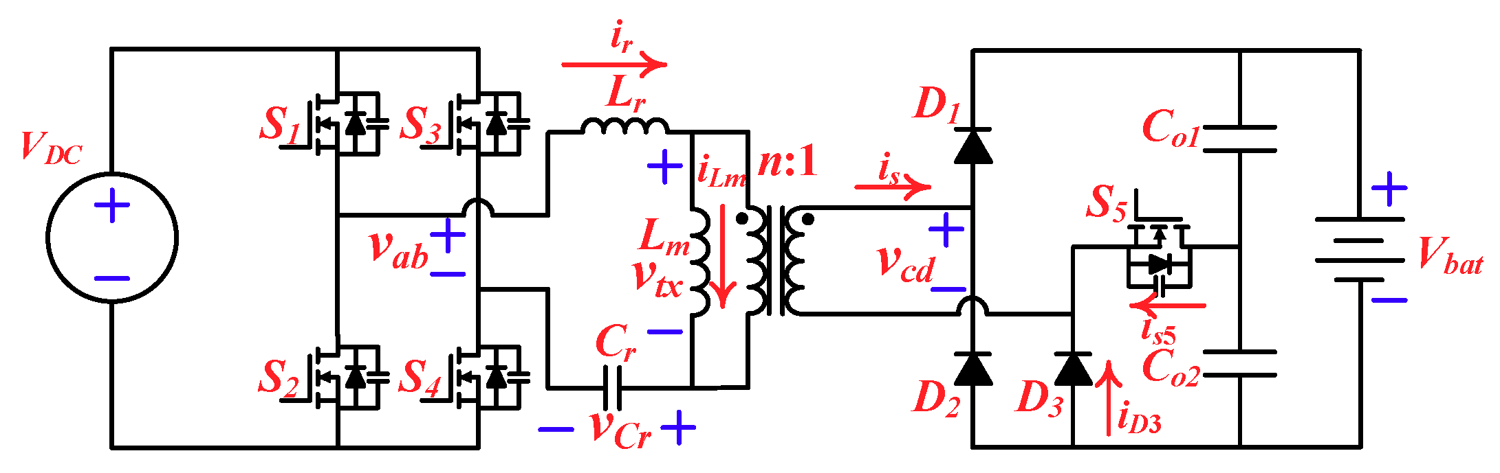
2.1. Topology Description
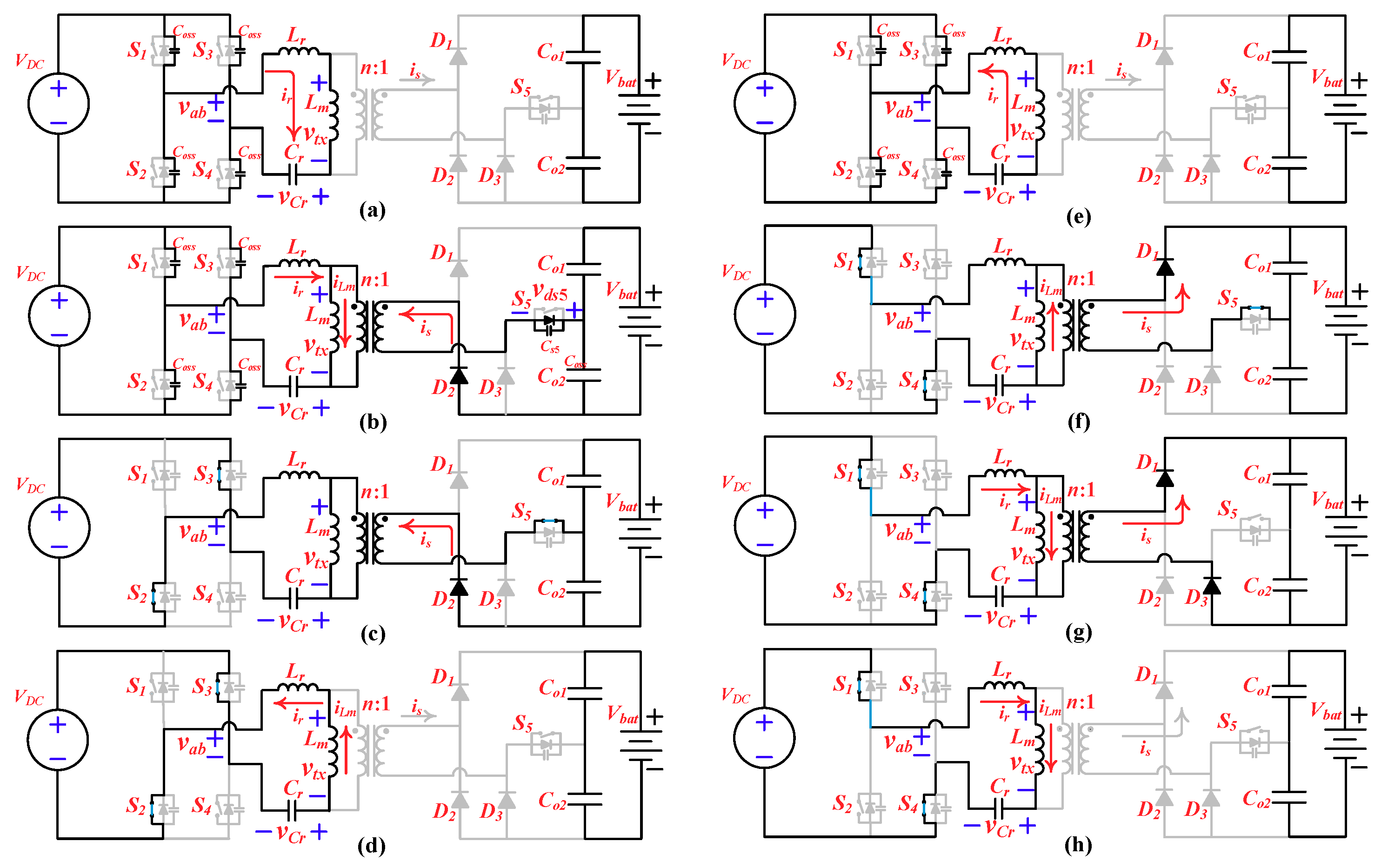
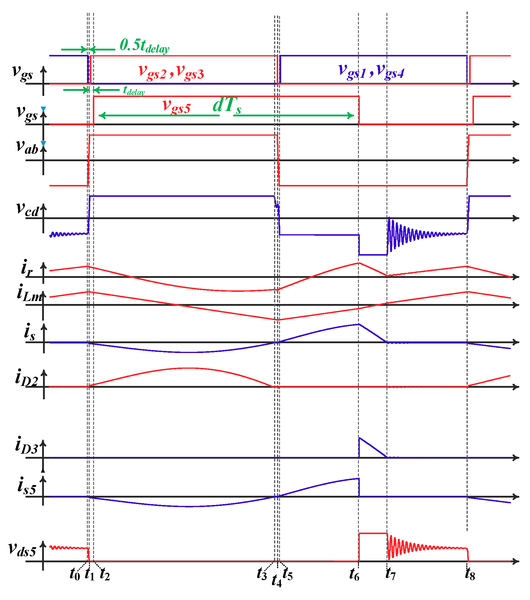
2.2. Operation Principle
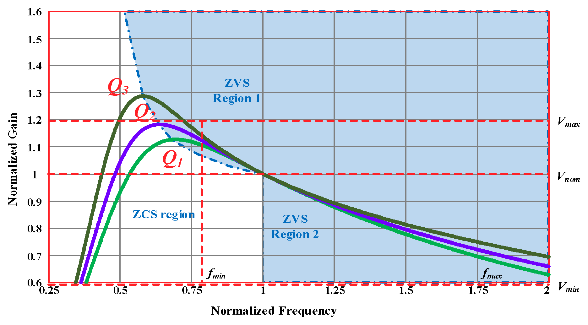
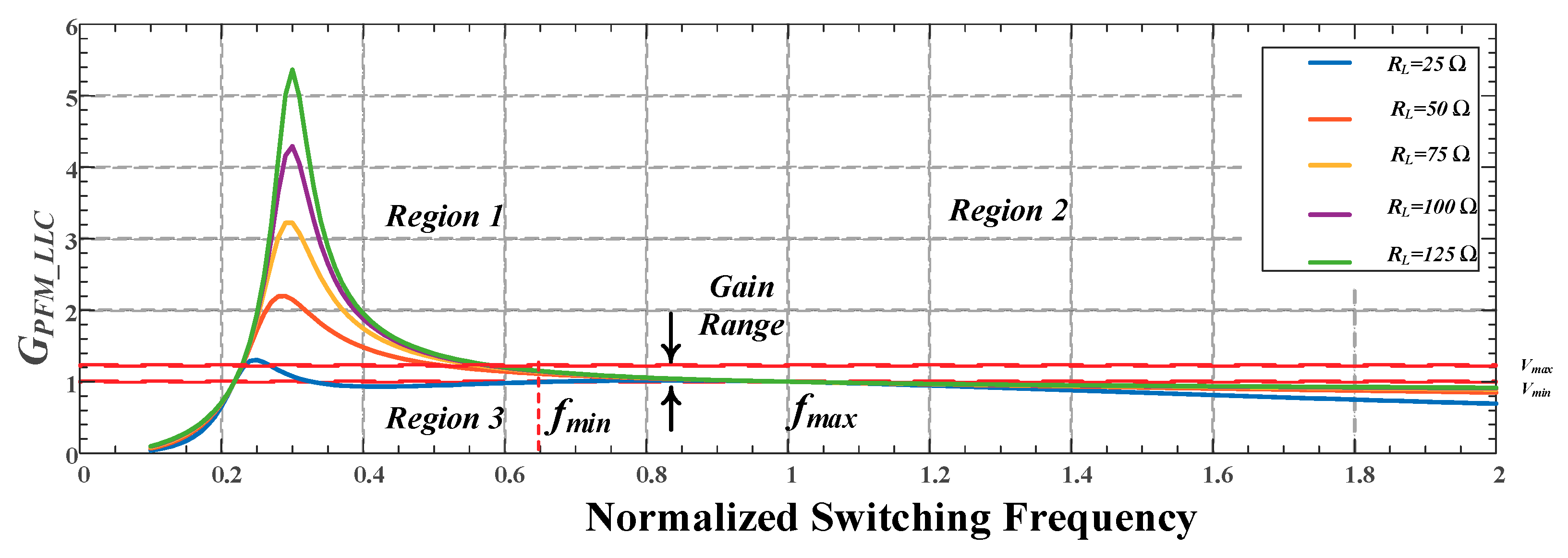
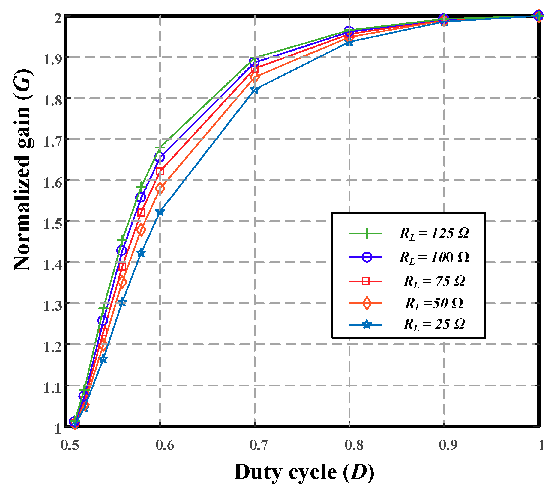
2.3. Gain Analysis
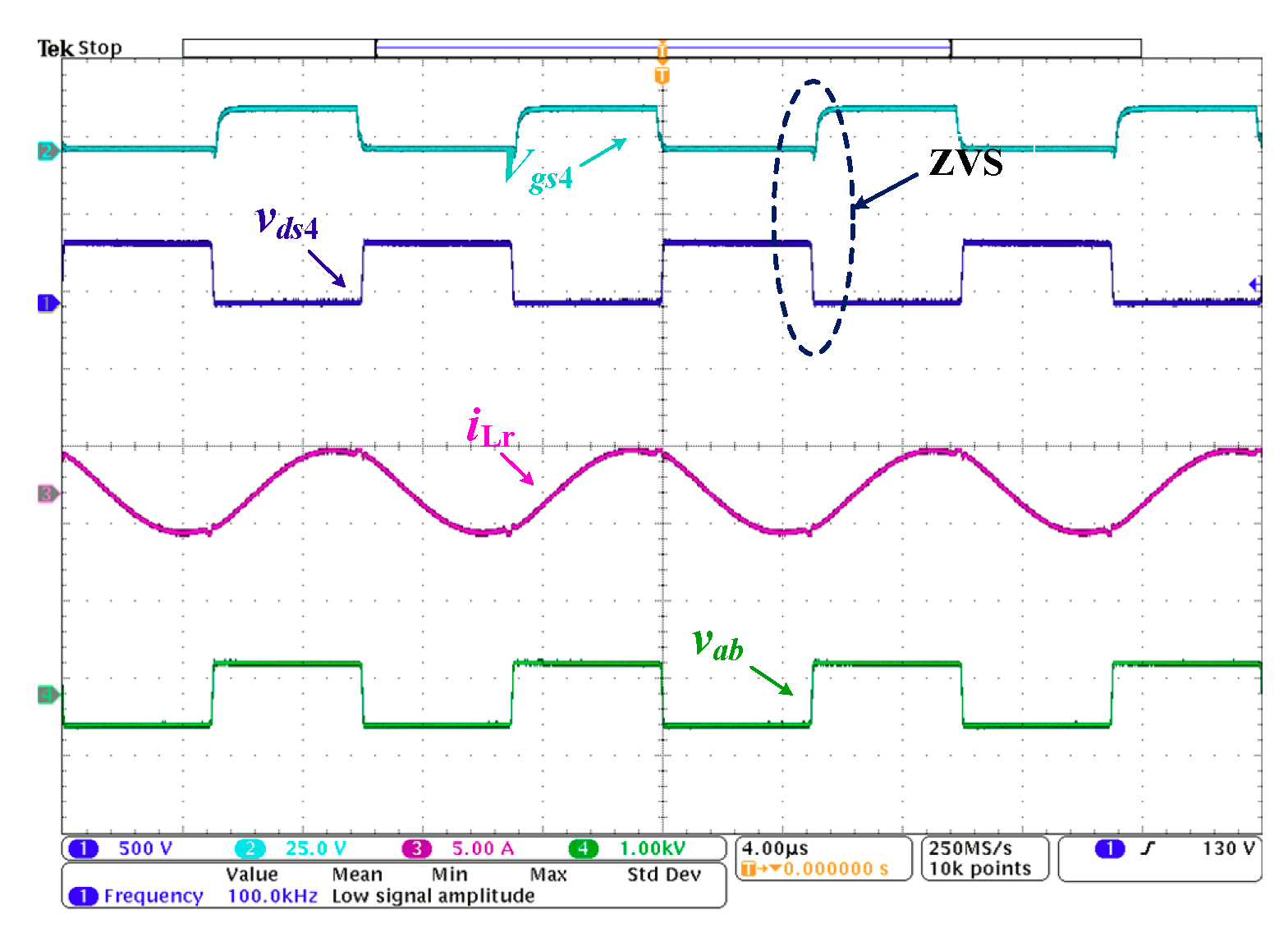
2.4. MOSFETs ZVS
3. Design Example
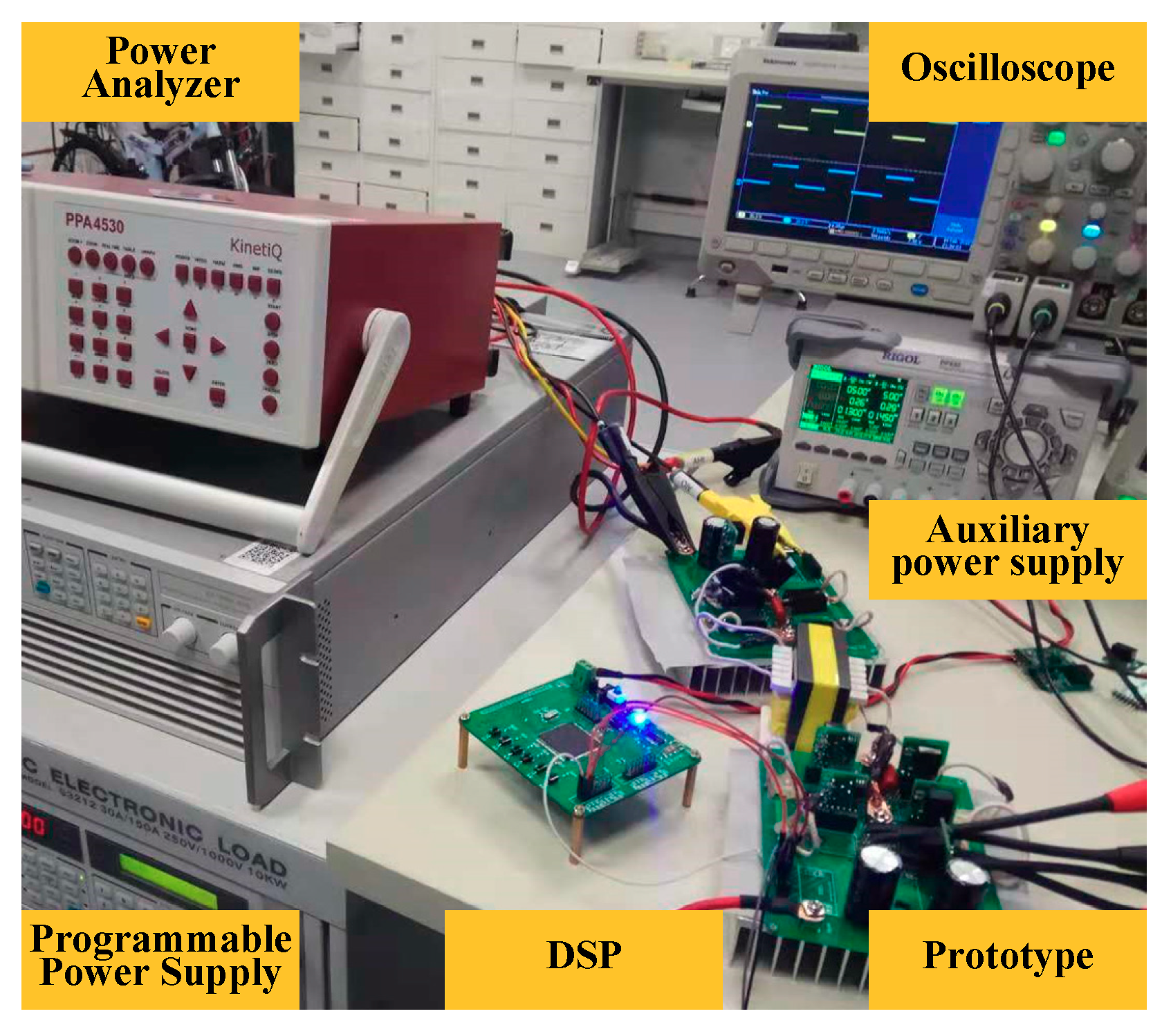
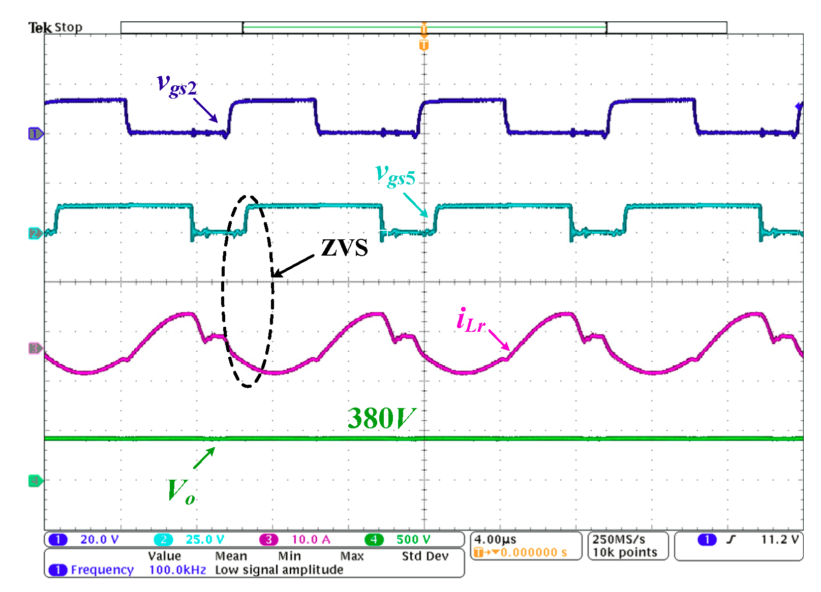
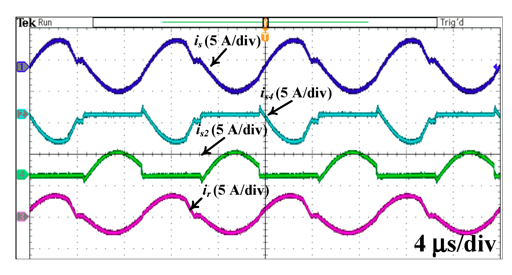
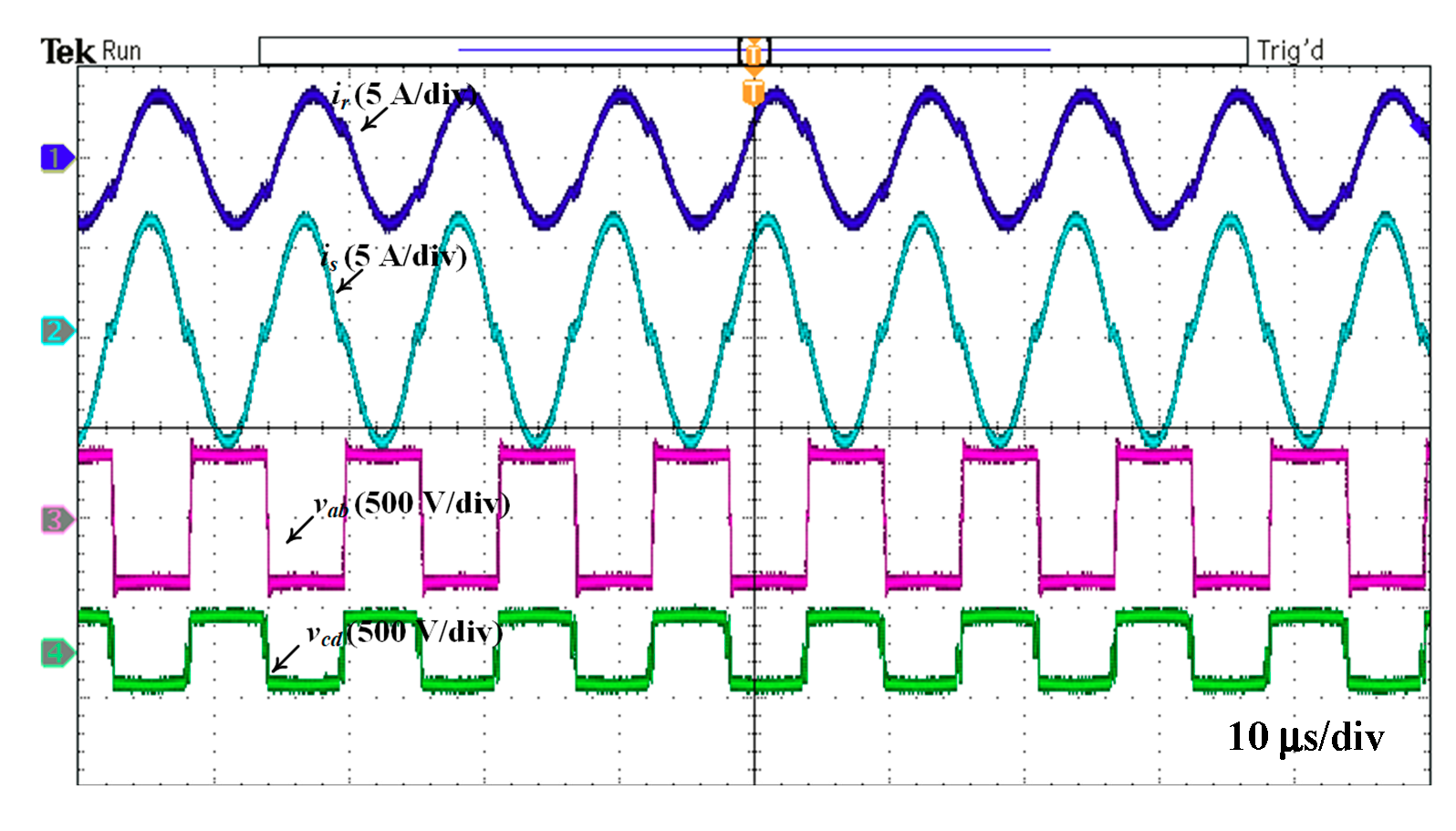
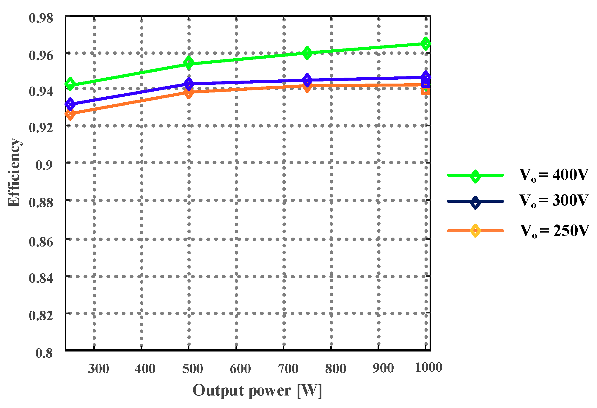
4. Experimental Results
5. Conclusions
Author Contributions
Funding
Conflicts of Interest
References
- Al-Alawi, B.M.; Bradley, T.H. Review of hybrid, plug-in hybrid, and electric vehicle market modeling Studies. Renew. Sustain. Energy Rev. 2013, 21, 190–203. [Google Scholar] [CrossRef]
- Yilmaz, M.; Krein, P.T. Review of battery charger topologies, charging power levels, and infrastructure for plug-in electric and hybrid vehicles. IEEE Trans. Power Electron. 2013, 28, 2151–2169. [Google Scholar] [CrossRef]
- Rubino, L.; Capasso, C.; Veneri, O. Review on plug-in electric vehicle charging architectures integrated with distributed energy sources for sustainable mobility. Appl. Energy 2017, 207, 438–464. [Google Scholar] [CrossRef]
- Fang, X.; Hu, H.; Shen, Z.J.; Batarseh, I. Operation mode analysis and peak gain approximation of the LLC resonant converter. IEEE Trans. Power Electron. 2012, 27, 1985–1995. [Google Scholar] [CrossRef]
- Khaligh, A.; Dusmez, S. Comprehensive Topological Analysis of Conductive and Inductive Charging Solutions for Plug-In Electric Vehicles. IEEE Trans. Veh. Technol. 2012, 61, 3475–3489. [Google Scholar] [CrossRef]
- Wang, H.; Li, Z. A PWM LLC type resonant converter adapted to wide output range in PEV charging applications. IEEE Trans. Power Electron. 2018, 33, 3791–3801. [Google Scholar] [CrossRef]
- Wu, H.; Zhan, X.; Xing, Y. Interleaved LLC Resonant Converter with Hybrid Rectifier and Variable-Frequency Plus Phase-Shift Control for Wide Output Voltage Range Applications. IEEE Trans. Power Electron. 2017, 32, 4246–4257. [Google Scholar] [CrossRef]
- Sun, X.; Shen, Y.; Zhu, Y.; Guo, X. Interleaved Boost-Integrated LLC Resonant Converter with Fixed-Frequency PWM Control for Renewable Energy Generation Applications. IEEE Trans. Power Electron. 2015, 30, 4312–4326. [Google Scholar] [CrossRef]
- Li, W.; Luo, Q.; Mei, Y.; Zong, S.; He, X.; Xia, C. Flying-Capacitor Based Hybrid LLC Converters with Input Voltage Auto-Balance Ability for High Voltage Applications. IEEE Trans. Power Electron. 2016, 31, 1908–1920. [Google Scholar] [CrossRef]
- Gautam, D.S.; Musavi, F.; Edington, M.; Eberle, W.; Dunford, W.G. An automotive onboard 3.3-kW battery charger for PHEV application. IEEE Trans. Veh. Technol. 2012, 61, 3466–3474. [Google Scholar] [CrossRef]
- Deng, J.; Li, S.; Hu, S.; Mi, C.C.; Ma, R. Design Methodology of LLC Resonant Converters for Electric Vehicle Battery Chargers. IEEE Trans. Veh. Technol. 2014, 63, 1581–1592. [Google Scholar] [CrossRef]
- Wang, H.; Dusmez, S.; Khaligh, A. Maximum Efficiency Point Tracking Technique for LLC-Based PEV Chargers Through Variable DC Link Control. IEEE Trans. Ind. Electron. 2014, 61, 6041–6049. [Google Scholar] [CrossRef]
- Lu, B.; Liu, W.; Liang, Y.; Lee, F.C.; van Wyk, J.D. Optimal Design Methodology for LLC Resonant Converter. In Proceedings of the IEEE Applied Power Electronics Conference and Exposition, Dallas, TX, USA, 19–23 March 2006. [Google Scholar]
- He, P.; Khaligh, A. Comprehensive Analyses and Comparison of 1 kW Isolated DC–DC Converters for Bidirectional EV Charging Systems. IEEE Trans. Transp. Electrif. 2017, 3, 147–156. [Google Scholar] [CrossRef]
- Kim, J.-W.; Moon, G.-W. A New LLC series resonant converter with a narrow switching frequency variation and reduced conduction losses. IEEE Trans. Power Electron. 2014, 29, 4278–4287. [Google Scholar] [CrossRef]
- Feng, W.; Lee, F.C.; Mattavelli, P. Optimal Trajectory Control of Burst Mode for LLC Resonant Converter. IEEE Trans. Power Electron. 2013, 28, 457–466. [Google Scholar] [CrossRef]
- Zhao, B.; Song, Q.; Liu, W.; Sun, Y. Overview of dual-active-bridge isolated bidirectional DC–DC converter for high-frequency-link power-conversion system. IEEE Trans. Power Electron. 2014, 29, 4091–4106. [Google Scholar] [CrossRef]
- Musavi, F.; Craciun, M.; Gautam, D.S.; Eberle, W. Control strategies for wide output voltage range LLC resonant DC–DC converters in battery chargers. IEEE Trans. Veh. Technol. 2014, 63, 1117–1125. [Google Scholar] [CrossRef]
- Shafiei, N.; Ordonez, M.; Craciun, M.; Botting, C.; Edington, M. Burst Mode Elimination in High Power LLC Resonant Battery Charger for Electric Vehicles. IEEE Trans. Power Electron. 2016, 31, 1173–1188. [Google Scholar] [CrossRef]
- Kim, B.; Park, K.; Moon, G. Asymmetric PWM Control Scheme during Hold-Up Time for Resonant Converter. IEEE Trans. Ind. Electron. 2012, 59, 2992–2997. [Google Scholar] [CrossRef]
- Lee, W.J.; Kim, C.E.; Moon, G.W.; Han, S.K. A new phase-shifted full-bridge converter with voltage-doubler-type rectifier for high-efficiency PDP sustaining power module. IEEE Trans. Ind. Electron. 2008, 55, 2450–2458. [Google Scholar]
- Kim, M.Y.; Kim, B.C.; Park, K.B.; Moon, G.W. LLC series resonant converter with auxiliary hold-up time compensation circuit. In Proceedings of the 8th International Conference on Power Electronics—ECCE Asia, Jeju, Korea, 30 May–3 June 2011; pp. 628–633. [Google Scholar]
- Ajmal, F.; Pan, H.; He, C.; Chen, G.; Chen, H. Pulse-width modulation control strategy for high efficiency LLC resonant converter with light load applications. IET Power Electron. 2014, 7, 2887–2894. [Google Scholar]
- Park, H.P.; Jung, J.H. PWM and PFM Hybrid Control Method for LLC Resonant Converters in High Switching Frequency Operation. IEEE Trans. Ind. Electron. 2017, 64, 253–263. [Google Scholar] [CrossRef]
- Hu, Y.; Wu, J.; Cao, W.; Xiao, W.; Li, P.; Finney, S.J.; Li, Y. Ultrahigh Step-up DC–DC Converter for Distributed Generation by Three Degrees of Freedom (3DoF) Approach. IEEE Trans. Power Electron. 2016, 31, 4930–4941. [Google Scholar]
- Beiranvand, R.; Rashidian, B.; Zolghadri, M.R.; Alavi, S.M.H. A design procedure for optimizing the LLC resonant converter as a wide output range voltage source. IEEE Trans. Power Electron. 2012, 27, 3749–3763. [Google Scholar] [CrossRef]
- Abdel-rahman, S. Resonant LLC Converter: Operation and Design; Infineon Technologies North America: Durham, NC, USA, 2012; pp. 1–19. [Google Scholar]


| Vo (V) Output | Modulation Mode | Inverter Side Configuration | Rectification Side Configuration | Operating Frequency |
|---|---|---|---|---|
| 200–400 | PWM | Full Bridge | PWM Controlled S5 | fr |
| 400–440 | PFM | Full Bridge | Voltage Doubler | <fr |
| Components | PWM-LLC |
|---|---|
| Resonant frequency (fr) | 100 kHz |
| Magnetizing inductor (Lm) | 200 mH |
| Resonant inductor (Lr) | 20 mH |
| Resonant capacitor (Cr) | 125 nF |
| Turns ratio (np:ns) | 30:15 |
| High voltage diodes (D1–2) | C3D10060A |
| High voltage MOSFETs (S1–4) | IRFP460 |
| Low voltage MOSFETs (S5) | FPQ22N30 |
| Filter capacitors (Co1, Co2) | 120 mF |
| Low voltage diode (D3) | MBR40250G |
© 2018 by the authors. Licensee MDPI, Basel, Switzerland. This article is an open access article distributed under the terms and conditions of the Creative Commons Attribution (CC BY) license (http://creativecommons.org/licenses/by/4.0/).
Share and Cite
Khalid, U.; Khan, M.M.; Khan, M.Z.; Usman Rasool, M.A.; Xu, J. Pulse Width and Frequency Hybrid Modulated LLC Converter Adapted to Ultra Wide Voltage Range. Inventions 2018, 3, 77. https://doi.org/10.3390/inventions3040077
Khalid U, Khan MM, Khan MZ, Usman Rasool MA, Xu J. Pulse Width and Frequency Hybrid Modulated LLC Converter Adapted to Ultra Wide Voltage Range. Inventions. 2018; 3(4):77. https://doi.org/10.3390/inventions3040077
Chicago/Turabian StyleKhalid, Umar, Muhammad Mansoor Khan, Muhammad Zahid Khan, Muhammad Ahmad Usman Rasool, and Jianming Xu. 2018. "Pulse Width and Frequency Hybrid Modulated LLC Converter Adapted to Ultra Wide Voltage Range" Inventions 3, no. 4: 77. https://doi.org/10.3390/inventions3040077
APA StyleKhalid, U., Khan, M. M., Khan, M. Z., Usman Rasool, M. A., & Xu, J. (2018). Pulse Width and Frequency Hybrid Modulated LLC Converter Adapted to Ultra Wide Voltage Range. Inventions, 3(4), 77. https://doi.org/10.3390/inventions3040077