Article

An Adaptive Bi-Band Doherty PA with Main-Peak Amplifier Swapping and Extended Bandwidth Performance

by
Jorge Julian Moreno Rubio
*,
Edison Ferney Angarita Malaver
and
Jairo Alonso Mesa Lara
Grupo de Investigación en Telecomunicaciones–GINTEL, Universidad Pedagógica y Tecnológica de Colombia, Sogamoso 152211, Colombia
*
Author to whom correspondence should be addressed.
Inventions 2025, 10(4), 69; https://doi.org/10.3390/inventions10040069
Submission received: 26 June 2025 / Revised: 22 July 2025 / Accepted: 6 August 2025 / Published: 8 August 2025

Abstract

This paper presents the design, implementation, and characterization of a broadband power amplifier (PA) with a reconfigurable architecture, capable of efficient operation across a wide frequency range of 0.2–3.6 GHz. Leveraging Gallium Nitride (GaN) devices, the PA achieves high efficiency and power, essential for broadband and high-frequency applications. By swapping the roles of the main and peak amplifiers, the PA achieves Doherty behavior at two related frequencies, 1.4 and 2.8 GHz, where the first is exactly half of the second, while maintaining consistent efficiency and output power across the remaining band in non-Doherty modes. Characterization results confirm the reliability and versatility of the proposed design, showcasing its ability to deliver robust performance across both Doherty and non-Doherty operational ranges. This combination of GaN technology and innovative reconfigurability makes the PA highly suitable for broadband applications requiring high efficiency, flexibility, and wideband coverage. Moreover, the simplicity of the proposed design makes it not only practical for implementation but also highly competitive among state-of-the-art solutions.

1. Introduction

Broadband power amplifiers (PAs) are crucial components in modern wireless communication systems, where efficiency and adaptability across wide frequency ranges are of paramount importance. Traditional PA architectures, including the Doherty Power Amplifier (DPA), have demonstrated remarkable performance in specific frequency bands, but their operation is often limited by narrowband design constraints [1,2,3,4,5,6,7,8,9,10,11,12,13].
The design of broadband and efficient DPAs has become a central focus in RF power amplifier research, particularly for 5G and future wireless communication systems. One innovative approach introduces a shunt λ / 2 microstrip line at the combiner of a traditional DPA, enabling wideband impedance transformation for the carrier amplifier. This technique enhances both bandwidth and back-off efficiency, achieving saturated output powers above 43 dBm and drain efficiencies between 65% and 72% across 3.1–3.7 GHz [2]. Similarly, a wideband class AB-C DPA design addresses the non-ideal output impedance of the auxiliary amplifier due to parasitic effects. By optimizing the output matching network, this design achieves a 25% fractional bandwidth (2.8–3.6 GHz), with saturated drain efficiencies up to 76.5% and strong linear gain performance [6].
Beyond traditional DPA architectures, alternative load modulation strategies have emerged to overcome inherent bandwidth limitations. The pseudo-Doherty Load-Modulated Balanced Amplifier (PD-LMBA) introduces a novel configuration that decouples the carrier and peaking amplifiers, enabling optimal load modulation with a static phase offset. This architecture achieves high efficiency (up to 72%) over a wide frequency range (1.5–2.7 GHz) and maintains 47–61% efficiency under modulated signals [5]. Complementing this, a simplified design methodology for broadband DPAs leverages linear simulations to estimate bandwidth and uses the device’s output capacitance to guide the Doherty combiner design. A GaN-based prototype using this method demonstrated an 87% bandwidth (1.5–3.8 GHz), with 6 dB back-off efficiencies between 33% and 55%, and confirmed linearizability under modulated signals [14].
This work focuses on the design, implementation, and characterization of a broadband PA that overcomes traditional limitations by incorporating a reconfigurable amplifier configuration and leveraging advanced Gallium Nitride (GaN) devices [14,15,16,17,18,19,20,21]. The proposed architecture allows the roles of the main and peak amplifiers to be interchanged, enabling the PA to achieve Doherty-like behavior at two harmonically related frequencies, 1.4 and 2.8 GHz, while maintaining consistent efficiency and output power across the broader 0.2–3.6 GHz range. These configurations optimize performance at targeted frequency bands and ensure reliable operation outside Doherty modes, effectively addressing challenges associated with broadband operation and delivering robust performance across varying conditions. Table 1 compares this work with several state-of-the-art DPAs, demonstrating that the proposed approach is competitive.

2. Design

2.1. Transmission Line Equivalence and Impedance Inversion

Let us consider the Capacitance-Inductance-Capacitance (CLC) low-pass network shown in Figure 1a, where a series inductor is placed between two shunt capacitors. This network behaves as an impedance inverter at a frequency ω 0 = 1 / ( L C ) . In addition, it exhibits characteristics similar to a transmission line with characteristic impedance Z 0 = L / C , over a range of frequencies up to ω 0 / ( 2 π ) GHz and beyond, due to the gentle slope near the cutoff frequency. To demonstrate this behavior, Figure 1b illustrates S 11 and S 21 for a low-pass CLC network with capacitors of 1.7 pF and Z 0 = 33 Ω , which means an inductor of 1.9 nH. In this case f 0 = ω 0 / ( 2 π ) = 2.8 GHz, it means a perfect matching at that frequency, as demonstrated by the sharp drop in S 11 in Figure 1b. The phase of S 21 is presented in Figure 1c, where a −90° response is obtained at 2.8 GHz.
Thus, the proposed CLC network, shown in Figure 1a, can emulate a 33 Ω transmission line. When terminated with the same 33 Ω , it achieves quasi-complete impedance matching with an input impedance of 33 Ω . Notably, this 33 Ω termination can be realized within a 50 Ω system by employing a real-to-real impedance transformation across an arbitrary bandwidth (with an arbitrary number of sections), valid for the frequency band from 0 to beyond ω 0 . Furthermore, assuming the capacitor C represents the typical output capacitance of a FET, this low-pass filter emerges as a compelling choice for achieving broadband matching, paving the way for the design of a broadband power amplifier.
In this framework, as anticipated, cascading the CLC network with an identical copy results in a 180° (at ω 0 ) equivalent transmission line with a characteristic impedance of 33 Ω . This approach can be effectively utilized to extend the equivalent length of the transmission line.

2.2. Utilizing the Equivalent Reactive Output Network of FETs to Emulate a Low-Pass CLC Network

As discussed in the literature [10,14,17,20], the equivalent output network of a FET is typically modeled as a shunt capacitor and a series inductor, referred to as C O and L O , respectively. These components can be employed to synthesize the CLC network illustrated in Figure 1a by incorporating an additional series inductor L x and a subsequent shunt capacitor with a value of C O . The inductance L x can be calculated using the following formula:
L x = Z 0 2 C O L O
Ensure that the value of L x remains positive by appropriately selecting the frequency ω 0 . Notice that L = Z 0 2 C O .
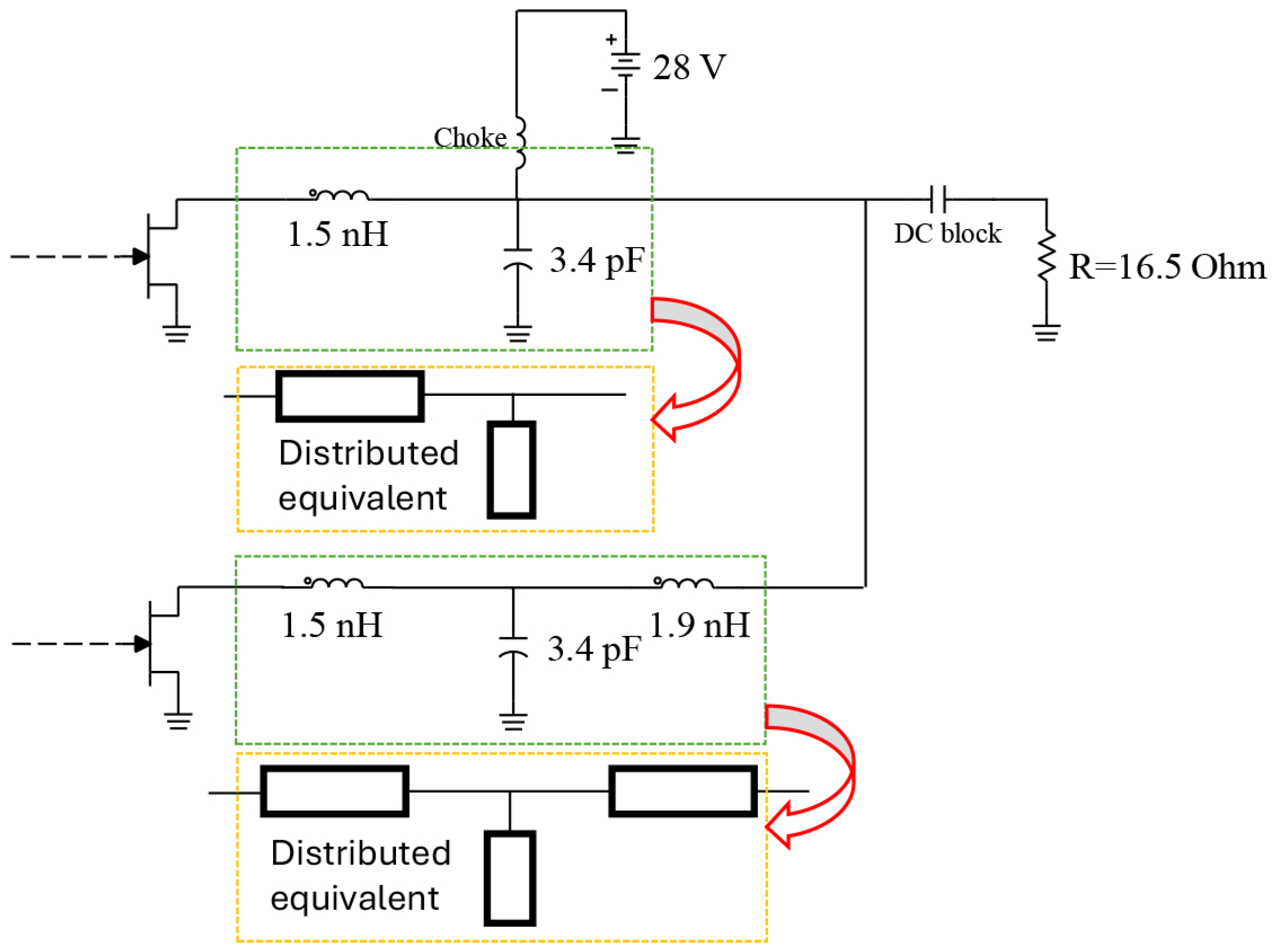
For implementation purposes, it is crucial to account for the challenges associated with incorporating lumped components, particularly when they must be directly connected to a transistor. Therefore, it becomes necessary to identify a distributed equivalent to replicate the effects of L x and C O beyond the drain pin of the transistor. Thus, the proposed distributed network considers a series transmission line followed by an open shunt transmission line, as will be shown later.

2.3. DPA Architecture Based on CLC Networks

Figure 2 illustrates the proposed Doherty Power Amplifier (DPA) combiner architecture based on the CLC network. The CLC network described in the previous section serves as the foundational element for the proposed Doherty Power Amplifier (DPA) architecture. In this configuration, the output matching network of the main amplifier branch is implemented using a single CLC section, effectively emulating a 90° (impedance inverter) transmission line with a characteristic impedance of Z 0 = 33 Ω . To achieve the necessary phase alignment and impedance transformation required for Doherty operation, the peak amplifier branch incorporates two cascaded CLC sections, thereby doubling the electrical length relative to the main path. This arrangement ensures a 90° phase shift between the main and peak paths at the chosen frequency, enabling proper load modulation and power combining. The outputs of both branches are combined at a common node and delivered to a transformed load impedance of Z 0 / 2 , consistent with Doherty operation principles. This impedance transformation ensures that the final 50 Ω system load is appropriately matched to the combiner.
In this case, the selected device for both the main and peak amplifiers is the CG2H40010. Consequently, the reactive output equivalent network is modeled with a capacitance of C O = 1.7 pF and an inductance of L O = 0.4 nH. The optimal impedance for this device is considered in this case of 33 Ω , while the selected frequency is 2.8 GHz. As shown in Figure 2, an inductor L x = 1.5 nH is connected directly to the drain pin of the device, forming a total inductance of 1.9 nH for the CLC network, as illustrated in Figure 1a. Following this, a 1.7 pF capacitor is shunted to complete the CLC network.
Note that in Figure 2, a 3.4 pF capacitor is depicted. This value represents the parallel combination of two 1.7 pF capacitors—one from the upper branch and the other from the lower branch. It is important to highlight that in the peak branch, the CLC network is synthesized twice to achieve the 180° phase shift required for the peak output.
In Figure 2, the gate bias voltages are indicated for each operating mode. For the frequency band from 0.2 to 1.5 GHz, the upper (peak) device is biased at −4 V, while the lower (main) device is biased at −2.7 V. For the band from 1.5 to 3.2 GHz, the upper device is biased at −2.7 V (main) and the lower one at −6 V (peak). These values were intentionally optimized to achieve the best DPA performance using the proposed configuration.
To achieve adequate input matching for both amplifiers in this preliminary design, a 10 Ω reference impedance has been adopted, as shown in Figure 2. A 10 Ω 90° transmission line is implemented in the main branch to adjust the current phase, ensuring proper signal combining at the output. An ideal even power divider with a 10 Ω reference impedance is also employed. In practice, using an even division ratio contributes to improved bandwidth performance [14].
Figure 3b presents the PAE and transducer gain profiles obtained for the proposed DPA structure at 2.8 GHz. As shown, a characteristic DPA performance is achieved. When the main and peak amplifiers are swapped and the simulation is repeated at 1.4 GHz, DPA profiles for both PAE and transducer gain are again observed, as illustrated in Figure 3a. This behavior is attributed to the 180° equivalent transmission line at 2.8 GHz in the lower branch, which becomes equivalent to a 90° transmission line at 1.4 GHz.
In the upper branch, the combiner structure introduces a 45° equivalent transmission line at 1.4 GHz, resulting in an imaginary impedance component for the lower amplifier at back-off. However, as seen in Figure 3a, this imaginary component does not degrade the efficiency profile, since the resulting impedance remains within the high-efficiency region. These results demonstrate the effectiveness of the proposed combiner in achieving bi-band DPA performance.
Additionally, some chokes are used as part of the bias circuit to eliminate the effects of the bias-tees on the PA’s bandwidth behavior. As can be observed, when both devices operate at maximum power, the load seen by each device is closely the optimal 33 Ω over the CLC network bandwidth. This characteristic of the combiner ensures broadband performance of the PA. Consequently, the design not only achieves a bi-band DPA but also functions as a broadband amplifier. Specifically, DPA behavior is observed near 1.4 and 2.8 GHz, while a combined PA behavior is exhibited outside these frequencies. The expected bandwidth of the PA extends from 0 to 3.5 GHz, which corresponds to the bandwidth of the CLC network.

3. Implementation and Characterization

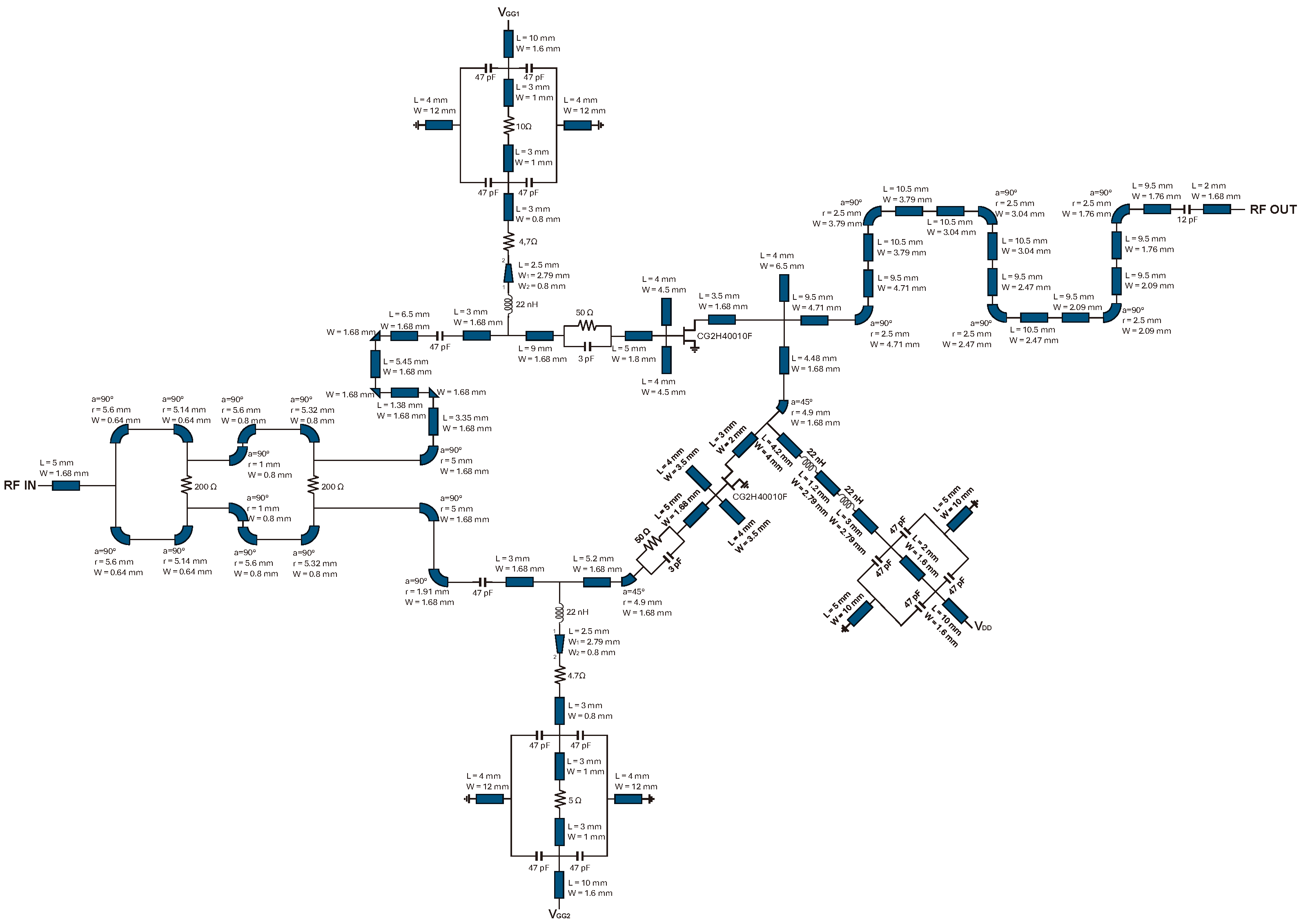
As mentioned earlier, it is necessary to transform the lumped components obtained from the CLC network into distributed elements, which are easier to implement on a typical substrate. In this case, the RF-35 Taconic substrate, with a relative dielectric constant of 3.5 and h = 0.76 mm, is used. A straightforward methodology is applied: each series inductor, together with a shunt capacitor, is replaced by a series transmission line and a shunt open-terminated transmission line, as shown in Figure 4. The widths and lengths of the transmission lines are tuned to replicate the response of the original lumped component network. Additionally, the chokes are implemented using high-value inductors, as illustrated in Figure 5. Note that the tail-like structure at the output of the circuit shown in the figure is a six-section transformer, designed to convert the 50 Ω system reference impedance to the 16.5 Ω required as the common load for the DPA.
The input matching network shown in Figure 2 is redesigned to have a 50 Ω reference. Additionally, a stabilization network is included, which is always necessary when working with this type of device.
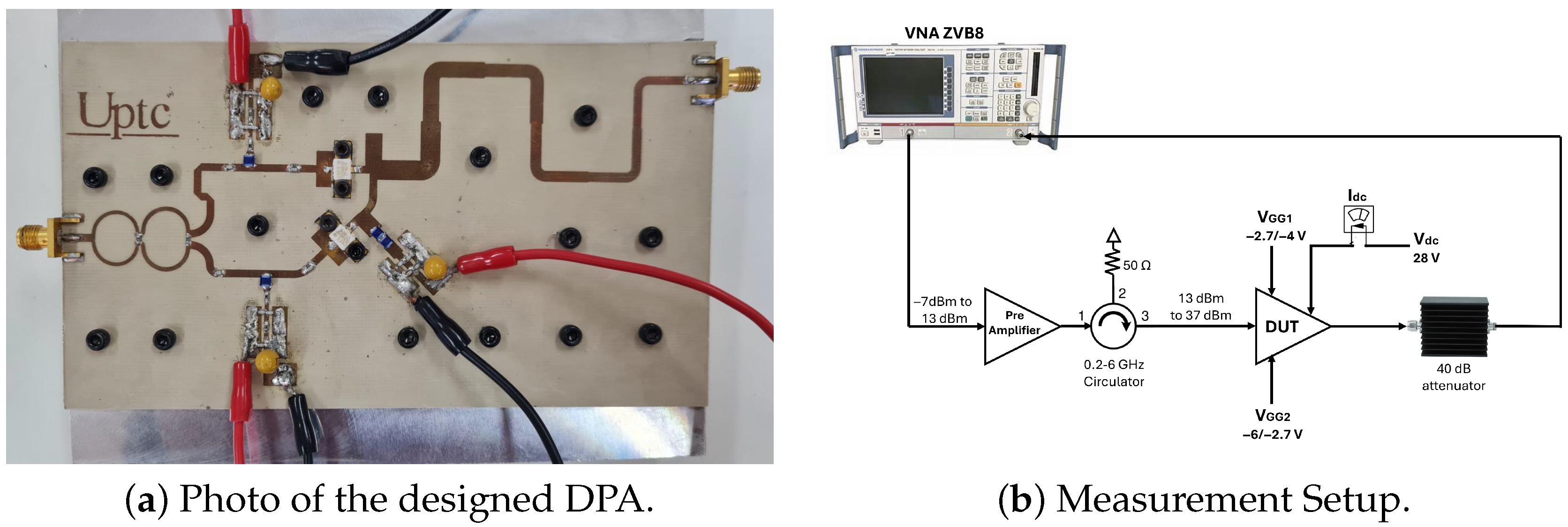
The complete schematic of the designed DPA is shown in Figure 5. This schematic was implemented, and a photograph of the fabricated circuit is also presented in Figure 6, along with a block diagram of the measurement setup. A continuous wave (CW) characterization was carried out. For the first band (0.2–1.5 GHz), the saturated transducer gain ranged from 8 to 14 dB, while the output power was between 41 and 44 dBm. The drain efficiency at 6 dB output back-off (OBO) ranged from 31% to 42%, and at saturation, it ranged from 60% to 72%. In the second band (1.5–3.5 GHz), where the main and peak amplifiers are swapped, the saturated transducer gain was between 8 and 10 dB, and the output power again ranged from 41 to 44 dBm. The drain efficiency at 6 dB OBO ranged from 30% to 42%, while at saturation it ranged from 42% to 52%. Some measured efficiency and gain profiles are presented in Figure 7. The results, including saturated output power, saturated gain, saturated drain efficiency, and drain efficiency at 6 dB of output back-off, are presented in Figure 8, alongside comparative simulation data.
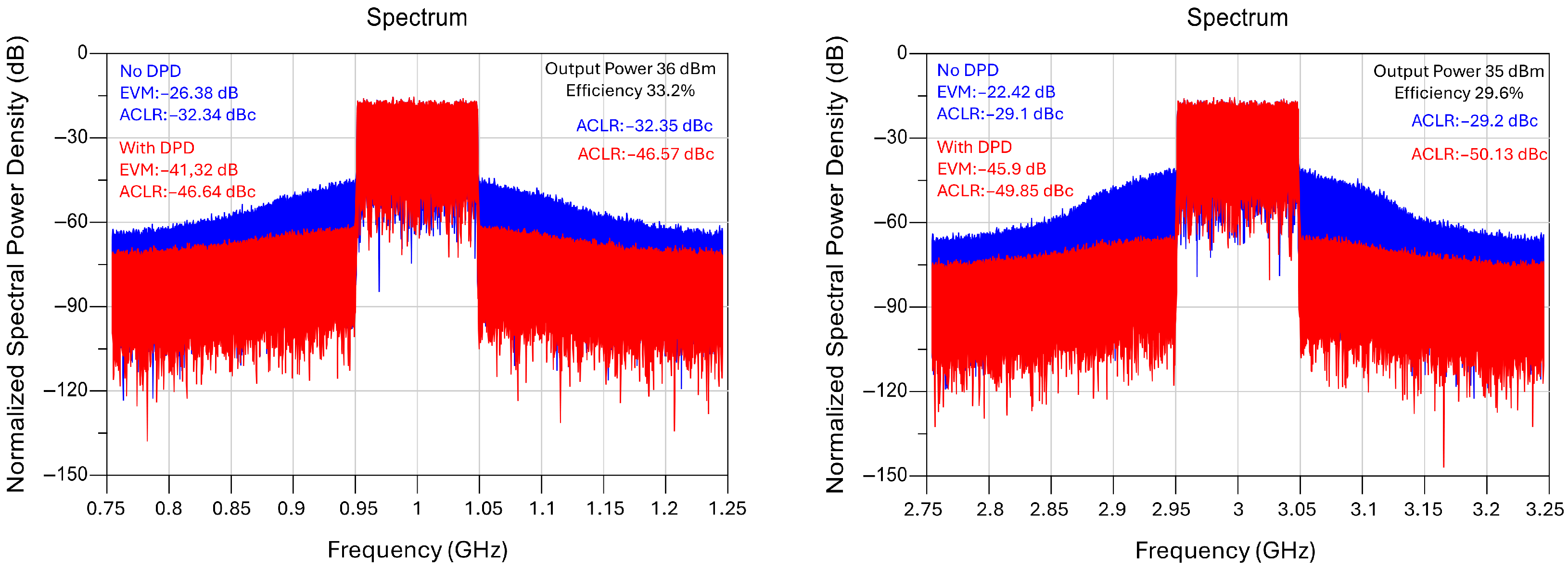
The system performance of the design was evaluated using the Keysight ADS 2025 DPD Explorer simulation tool, employing a Generalized Memory Polynomial (GMP) model with a memory depth of 3 and an order of 7. This model is robust across wideband signals, ensuring effective linearization even under bandwidth expansion [22]. The simulation involved two 100 MHz 5G NR signals with carrier frequencies of 1 and 3 GHz, a Peak-to-Average Power Ratio (PAPR) of 9 dB, and an average available power of 24 dBm.
As shown in Figure 9, the results compare the power spectral density of the PA output with and without the application of Digital Predistortion (DPD). The application of DPD significantly improved the Adjacent Channel Leakage Ratio (ACLR), increasing it from 32.3 to 46.6 dBc at 1 GHz, and from 29.2 to 50.1 dBc at 3 GHz. Similarly, the Error Vector Magnitude (EVM) improved from −26.38 to −47.32 dB at 1 GHz, and from −22.42 to −46.5 dB at 3 GHz. The average simulated output power was 36 dBm for 1 GHz and 35 dBm for 3 GHz, with a PAE averaging approximately 33% and 30% respectively.

4. Conclusions

This work has introduced a reconfigurable broadband power amplifier architecture that effectively combines the benefits of Doherty operation with the flexibility of wideband performance. By strategically swapping the roles of the main and peak amplifiers, the design achieves efficient Doherty behavior at two harmonically related frequencies while maintaining consistent performance across the entire 0.2–3.6 GHz range. The use of GaN technology further enhances the amplifier’s power and efficiency, making it well-suited for demanding broadband applications. Experimental results validate the robustness and adaptability of the proposed solution. Most notably, the simplicity of the architecture not only facilitates practical implementation but also positions it as a highly competitive alternative among state-of-the-art designs.

Author Contributions

Conceptualization, J.J.M.R., E.F.A.M. and J.A.M.L.; Methodology, J.J.M.R.; Software, E.F.A.M. and J.A.M.L.; Validation, J.J.M.R., E.F.A.M. and J.A.M.L.; Formal analysis, J.J.M.R.; Investigation, J.J.M.R., E.F.A.M. and J.A.M.L.; Writing—original draft, J.J.M.R., E.F.A.M. and J.A.M.L.; Visualization, E.F.A.M. and J.A.M.L.; Supervision, J.J.M.R. All authors have read and agreed to the published version of the manuscript.

Funding

This research received no external funding.

Acknowledgments

We gratefully acknowledge the support of Christopher Groetsch and Robert Eichner from Keysight Technologies for their guidance on using the DPD Explorer in ADS.

Conflicts of Interest

The authors declare no conflict of interest.

References

  1. Ardekani, M.H.M.; Abiri, H. A new design procedure for wide band Doherty power amplifiers. AEU–Int. J. Electron. Commun. 2018, 98, 181–190. [Google Scholar] [CrossRef]
  2. Zhang, Z.; Cheng, Z.; Liu, G.; Zhang, Z.; Cai, Y. Design of a broadband high-efficiency doherty power amplifier for 5G communication systems. IEICE Electron. Express 2019, 16, 20190371–20190371. [Google Scholar] [CrossRef]
  3. Jia, P.; You, F.; He, S. A 1.8-3.4-GHz Bandwidth-Improved Reconfigurable Mode Doherty Power Amplifier Utilizing Switches. IEEE Microw. Wirel. Compon. Lett. 2019, 30, 102–105. [Google Scholar] [CrossRef]
  4. Nikandish, G.; Staszewski, R.B.; Zhu, A. Breaking the bandwidth limit: A review of broadband doherty power amplifier design for 5G. IEEE Microw. Mag. 2020, 21, 57–75. [Google Scholar] [CrossRef]
  5. Cao, Y.; Chen, K. Pseudo-Doherty Load-Modulated Balanced Amplifier with Wide Bandwidth and Extended Power Back-Off Range. IEEE Trans. Microw. Theory Tech. 2020, 68, 3172–3183. [Google Scholar] [CrossRef]
  6. Nasri, A.; Estebsari, M.; Toofan, S.; Piacibello, A.; Pirola, M.; Camarchia, V.; Ramella, C. Design of a wideband doherty power amplifier with high efficiency for 5G application. Electronics 2021, 10, 873. [Google Scholar] [CrossRef]
  7. Fu, C.; Wang, N.; Chen, X.; Chen, W. A Concurrent Dual-band Continuous Mode Doherty Power Amplifier with Improved Bandwidth and Linearity for 5G Base-Stations. In Proceedings of the 2022 IEEE Conference on Antenna Measurements and Applications (CAMA), Guangzhou, China, 14–17 December 2022; pp. 1–4. [Google Scholar] [CrossRef]
  8. Haider, J.; Zhou, H.; Saad, P.; Hou, R.; Fager, C. Design and Validation of a Concurrent Dual-Band 1.84/2.65 GHz GaN Doherty Power Amplifier. In Proceedings of the 2023 International Workshop on Integrated Nonlinear Microwave and Millimetre-Wave Circuits (INMMIC), Aveiro, Portugal, 8–11 November 2023; pp. 1–4. [Google Scholar] [CrossRef]
  9. Zhong, K.; Dai, Z.; Xiao, F.; Gao, R.; Shi, W.; Pang, J.; Li, M. Design of Dual-Band Doherty Power Amplifier Using a New Phase Compensation Technique. IEEE Trans. Circuits Syst. II Express Briefs 2024, 71, 1794–1798. [Google Scholar] [CrossRef]
  10. Rubio, J.J.M.; Noori, A. Doherty Power Amplifier Design via Differential Combining. Electronics 2024, 13, 3961. [Google Scholar] [CrossRef]
  11. Piacibello, A.; Camarchia, V. High-Efficiency GaN Doherty Power Amplifier based on Inverse Class-F Operation. In Proceedings of the 2024 IEEE Topical Conference on RF/Microwave Power Amplifiers for Radio and Wireless Applications, San Antonio, TX, USA, 21–24 January 2024; pp. 5–8. [Google Scholar] [CrossRef]
  12. Sun, P.; Han, F.; Liu, Z.; Qi, Q.; Li, X.; Wang, X. A Broadband Doherty Power Amplifier Design with 22.4-dBm Psat and 31% PAE in 45-nm SOI CMOS for 5G Application. IEEE Inf. Technol. Mechatron. Eng. Conf. ITOEC 2025, 8, 1075–1079. [Google Scholar] [CrossRef]
  13. Tao, M.; Chen, Y.; Kong, W.; Ni, S.; Zheng, Z.; Xia, J. Design of Dual-Mode Multi-Band Doherty Power Amplifier Employing Impedance-and-Phase Constrained Optimization. Electronics 2025, 14, 2078. [Google Scholar] [CrossRef]
  14. Rubio, J.J.M.; Camarchia, V.; Pirola, M.; Quaglia, R. Design of an 87% Fractional Bandwidth Doherty Power Amplifier Supported by a Simplified Bandwidth Estimation Method. IEEE Trans. Microw. Theory Tech. 2017, 66, 1319–1327. [Google Scholar] [CrossRef]
  15. Chen, S.; Xue, Q. Compact triple-transistor doherty amplifier designs: Differential/power combining. IEEE Trans. Microw. Theory Tech. 2013, 61, 1957–1963. [Google Scholar] [CrossRef]
  16. Mohamed, A.M.M.; Boumaiza, S.; Mansour, R.R. Reconfigurable doherty power amplifier for multifrequency wireless radio systems. IEEE Trans. Microw. Theory Tech. 2013, 61, 1588–1963. [Google Scholar] [CrossRef]
  17. Giofre, R.; Piazzon, L.; Colantonio, P.; Giannini, F.; Camarchia, V.; Quaglia, R.; Pirola, M.; Ramella, C. GaN-MMIC Doherty power amplifier with integrated reconfigurable input network for microwave backhaul applications. In Proceedings of the 2015 IEEE MTT-S International Microwave Symposium, Phoenix, AZ, USA, 17–22 May 2015; pp. 2–4. [Google Scholar] [CrossRef]
  18. Kalyan, R.; Rawat, K.; Koul, S.K. Design of reconfigurable concurrent dual-band power amplifiers using reconfigurable concurrent dual-band matching network. In Proceedings of the 2016 IEEE MTT-S International Wireless Symposium (IWS), Shanghai, China, 14–16 March 2016; pp. 1–4. [Google Scholar] [CrossRef]
  19. Darraji, R.; Bhaskar, D.; Sharma, T.; Helaoui, M.; Mousavi, P.; Ghannouchi, F.M. Generalized Theory and Design Methodology of Wideband Doherty Amplifiers Applied to the Realization of an Octave-Bandwidth Prototype. IEEE Trans. Microw. Theory Tech. 2017, 65, 3014–3023. [Google Scholar] [CrossRef]
  20. Ramella, C.; Piacibello, A.; Quaglia, R.; Camarchia, V.; Pirola, M. High efficiency power amplifiers for modern mobile communications: The load-modulation approach. Electronics 2017, 6, 96. [Google Scholar] [CrossRef]
  21. Joonhyung, K. Highly Efficient Asymmetric Class-F-1/F GaN Doherty Amplifier. IEEE Trans. Microw. Theory Tech. 2018, 66, 4070–4077. [Google Scholar] [CrossRef]
  22. Liu, Y.-J.; Zhou, J.; Chen, W.; Zhou, B.-H. A Robust Augmented Complexity-Reduced Generalized Memory Polynomial for Wideband RF Power Amplifiers. IEEE Trans. Ind. Electron. 2014, 61, 2389–2401. [Google Scholar] [CrossRef]
Figure 1. A CLC network which mimics a transmission line up to beyond ω 0 , with Z 0 = 25 Ω .
Inventions 10 00069 g001
Figure 2. Lumped components DPA combiner structure.
Inventions 10 00069 g002
Figure 3. CW simulation of the DPA using the proposed Lumped components combiner.
Inventions 10 00069 g003
Figure 4. Lumped to distributed components transformation.
Inventions 10 00069 g004
Figure 5. Schematic of the implemented DPA.
Inventions 10 00069 g005
Figure 6. Photo of the circuit and setup measurement.
Inventions 10 00069 g006
Figure 7. Measured efficiency and gain profiles.
Inventions 10 00069 g007
Figure 8. CW characterization of DPA over the band.
Inventions 10 00069 g008
Figure 9. Normalized output power spectral density of the designed PA at 1 GHz and 3 GHz carrier frequency, with and without DPD.
Inventions 10 00069 g009
Table 1. Comparison with State-of-the-Art DPAs.
Ref[14][2][5][6]This Work
BW (GHz)1.5–3.83.1–3.71.5–2.72.8–3.60.2–3.6
D E @ O B O (%)33–55 @6 dB40–45 @8 dB47–61 @6 dB44–56 @6 dB30–44 @6 dB
D E s a t (%)42–6365–7258–7262–76.541–72
P O U T (dBm)42.3–43.443.13–44.654343–44.241–44.5
S. Gain (dB)10–13.89–9.56–118–13.58–14
Disclaimer/Publisher’s Note: The statements, opinions and data contained in all publications are solely those of the individual author(s) and contributor(s) and not of MDPI and/or the editor(s). MDPI and/or the editor(s) disclaim responsibility for any injury to people or property resulting from any ideas, methods, instructions or products referred to in the content.