
Article

High-Resolution Quad-Channel Picoammeter: Characterization and Commissioning †

by
Lucas Yugo Tanio
,
Maurício Martins Donatti
*,
Fernando Henrique Cardoso
,
Patricia Henriques Nallin
,
Vinicius Silva Oliveira
,
James Rezende Piton
and
Aline Ribeiro Passos
Brazilian Synchrotron Light Laboratory (LNLS), Brazilian Center of Research in Energy and Materials (CNPEM), Polo II de Alta Tecnologia—R. Giuseppe Máximo Scolfaro, 10000—Bosque das Palmeiras, Campinas, São Paulo 13085-903, Brazil
*
Author to whom correspondence should be addressed.
This article is a revised and expanded version of a paper entitled “High-resolution quad-channel picoammeter: characterization and commissioning”, which was presented at IBIC2024, Beijing, China, 9–13 September 2024, https://doi.org/10.18429/JACoW-IBIC2024-WEP64.
Instruments 2026, 10(2), 32; https://doi.org/10.3390/instruments10020032
Submission received: 26 April 2026 / Revised: 28 May 2026 / Accepted: 3 June 2026 / Published: 9 June 2026
(This article belongs to the Section Particle Detectors and Accelerators)

Abstract

To address the high demand for precise low-current measurements at the Sirius’ beamlines, a quad-channel high-resolution Ethernet picoammeter has been designed. The instrument can measure currents ranging from femtoampere to milliampere across eight selectable ranges, featuring integrated analog-to-digital converters (ADCs), enabling sampling rates of up to 2 ksps and synchronization capabilities. This work describes the hardware design, the hardware handling procedures to achieve sub-picoampere resolution, and the characterization results of the instrument, considering the experimental results from Sirius beamlines. The designed device provides noise performance and gain accuracy that is comparable to high-end commercial solutions, proving its suitability for critical applications like on-the-fly scanning experiments. Special attention will be given to evaluating trigger latency, synchronization outcomes, as well as the device’s installation and commissioning at beamlines. Furthermore, we will deeply explore the interplay between the trigger period, digital filter bandwidth, and front-end analog bandwidth to optimize the signal-to-noise ratio in specific applications. The hardware project is publicly available in CERN’s open hardware repository.

1. Introduction

The construction of Sirius [1], the Brazilian fourth-generation synchrotron light source, brought new challenges to the scientific and engineering areas. A highly demanded instrument in Sirius’ beamlines, the experimental station, is responsible for light beam diagnostics. At present, there are approximately one hundred monitors installed across thirteen beamlines (under commissioning or fully operational), and this number is expected to double in the next couple of years with the assembly of ten new beamlines. Most of the diagnostic elements (or sensors), such as photodiodes, ionization chambers, or X-ray beam position monitors (XBPMs) [2], convert synchrotron light into electrical current with different characteristics of amplitude and time response. Electronic devices for four-channel measurements are available, typically designed for XBPM applications and employing different current measurement topologies, such as transimpedance amplifiers (TIAs) [3] or charge integrators [4]. Charge-integrator-based devices implemented with discrete electronics present additional challenges, including the impact of amplifier leakage current, matching of reset conditions between channels, and the need to manage operation across wait, reset, integrate, and convert phases. Single integrated circuits (IC) solutions, such as DDC114 (Texas Instruments, Dallas, TX, USA) [5], are often preferred for this topology; however, they are generally limited to unipolar currents and face challenges when handling currents above hundreds of μA. In contrast, the TIA topology is more versatile, as it supports a broader range of input currents and does not require dedicated circuitry to manage amplification and conversion phases. This approach was, therefore, adopted for the device presented in this work.
Some of these systems are commercially available off the shelf [3,4,6], while others have been developed by research laboratories [7,8,9]. However, custom-designed devices are often required to enable native integration with beamline control systems. Commercial instruments are typically provided as closed-box solutions, limiting the implementation of modifications that could significantly improve performance in specific scientific applications. For example, the AH501D (CAEN ELS, Basovizza, Trieste, Italy) [3] is a quad-channel picoammeter; however, in multi-photodiode measurements, it is common for currents to differ by several orders of magnitude between channels, and the device does not support independent range configuration per channel.
Considering this scenario and addressing the high volume of current measurements required, where the scientific requirements necessitate current measurements with femtoampere resolutions, synchronization capabilities, and commercial instrumentation available are expensive or unsuitable due to performance or incompatible infrastructure, the Electronic Instrumentation Group (GIE) from the Brazilian Synchrotron Light Laboratory (LNLS/CNPEM) has designed a novel solution.
This paper describes the quad-channel high-resolution Ethernet picoammeter [10,11] designed by GIE. It details the hardware design, focusing on the analog front-end, the essential hardware procedures used to achieve sub-picoampere measurements, and the comprehensive characterization results of the instrument. Special attention is given to the features that enable data stream acquisition and front-end analog bandwidth, as well as the time requirements in the acquisition process and their limitations to optimize the signal-to-noise ratio (SNR) across the instrument’s eight selectable ranges.
The measured noise in the four most sensitive ranges is dominated by the thermal noise of the feedback resistor, reaching the intrinsic limit of the TIA topology [12]. In the remaining four ranges, noise performance is limited by the ADC resolution [11]. As a result, the overall measured noise is comparable to that of high-end commercial solutions employing 24-bit ADCs and TIAs. However, the proposed design offers a greater number of measurement ranges, providing increased flexibility. In addition, an individual calibration procedure—used to store offset and gain compensation values in the EEPROM [11]—is integrated into the hardware validation process, enabling a gain accuracy of approximately 0.1%.
The designed device demonstrates its suitability for critical applications like on-the-fly scanning experiments. Additionally, this work describes the installation and commissioning of the device at the Sirius beamlines and experimental results.
The remainder of this paper is organized as follows: Section 2 details the instrument’s hardware design, the importance of open hardware, and hardware handling and maintenance for low-current measurements. Special attention is also given to the design of the firmware and software architecture, with an in-depth presentation of the adopted data streaming and synchronization solutions. Section 3 presents the characterization and application results, including the analysis of the relationship among key performance metrics and scientific results obtained using the device in Sirius beamlines. Finally, Section 4 discusses current challenges and future steps, followed by the concluding remarks in Section 5.

2. Materials and Methods

2.1. Hardware Design

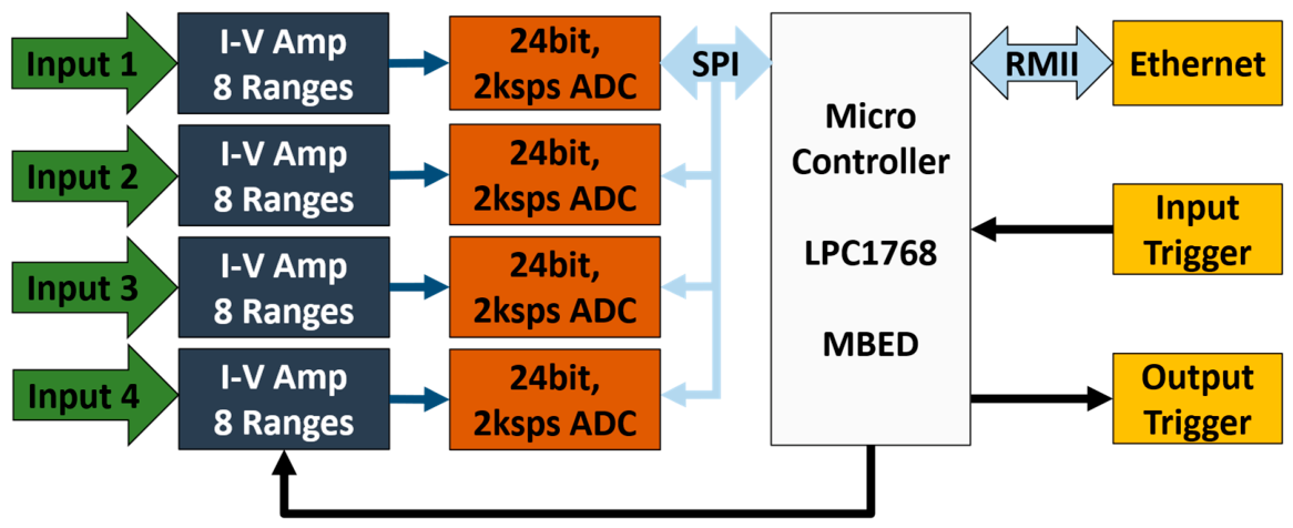
The quad-channel picoammeter comprises four key blocks: a current-to-voltage amplifier, an ADC, a microcontroller, and the external interface, as shown in the simplified block diagram in Figure 1. The detailed device architecture of the quad-channel picoammeter is discussed in [11].

2.1.1. Analog Front-End Circuit

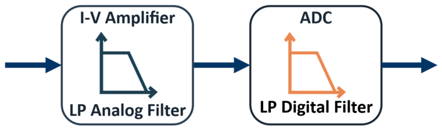
For each independent channel, an analog front-end circuit consists of two essential blocks: the current-to-voltage amplifier and the ADC that digitizes the output voltage from the first block. It is important to note that, in addition to current conversion and digitization, both blocks also act as low-pass filters, as illustrated in Figure 2.

2.1.2. Current-to-Voltage Amplifier

The multirange transimpedance amplifier was chosen for current-to-voltage conversion because of its wide measurement range, suitability for low bandwidth applications, and noise performance, as discussed in [10,11,12]. Each current-to-voltage converter features eight selectable ranges with specific characteristics. Table 1 presents the theoretical values of the full-scale, sensitivity, and bandwidth characteristics for each selectable range.

2.1.3. Analog-to-Digital Converter

Considering most beamline applications, high-resolution and low-speed acquisitions are typical requirements; therefore, the ADS1246 analog-to-digital converter (Texas Instruments, Dallas, TX, USA) [13] has been selected as the ADC for the electrometer. The component features a Σ-Δ topology, 24-bit resolution, and 10 selectable sampling rates from 5 SPS to 2000 SPS. Due to the Σ-Δ topology, for each selectable sampling rate, two important parameters are defined: the oversampling ratio (OSR) and the characteristics of the integrated digital filter.
The sampling frequency selection should be performed wisely by the user, as there is an inherent trade-off that affects the measurement resolution, the signal-to-noise ratio (SNR), and the signal bandwidth: higher sampling frequencies increase the measurement bandwidth, which allows the proper reading of faster signals, but at the cost of higher integrated noise and a lower OSR. Conversely, selecting a lower sampling frequency increases the OSR and narrows the bandwidth, effectively reducing the noise floor to maximize resolution and the SNR. The details of the characterization results of the bandwidth and noise are discussed in Section 3.1.

2.1.4. Microcontroller

The microcontroller, an LPC1768 microcontroller (NXP Semiconductors, Eindhoven, The Netherlands), supplied by Digi-Key Electronics (Thief River Falls, MN, USA) [14], that features a 32-bit ARM Cortex-M3 core operating at up to 100 MHz with I/O capabilities, handles peripheral configuration, manages ADC data acquisition, and oversees communication for the control software infrastructure.
However, recognizing that the NXP LPC1768 is intended for obsolescence in the coming years, and given its design limitations, such as limited RAM capacity, the number of available I/O ports, and aging peripherals, the Electronics Instrumentation Group has developed an in-house microcontroller board named Caju [15], which is a new platform based on the powerful STM32H7 series (STMicroelectronics, Geneva, Switzerland) [16]. This new board features an Arm Cortex-M7 core operating at 480 MHz, 1 MB of RAM, 2 MB of Flash memory, and modern peripherals, including a 16-bit ADC, Quad-SPI interface, USB OTG, Ethernet, and CAN FD. Furthermore, Caju has been designed to be pin-compatible with the NXP board to facilitate transparent hardware migration.

2.1.5. Input and Output Triggers

The most significant external interface in this application, apart from the communication, is the trigger interface. The picoammeter features an input optocoupler trigger that accepts a voltage range from 3.3 V to 27 V and has a minimum pulse width of hundreds of nanoseconds. It also includes an output trigger that is capable of driving a 50 Ω load at 5 V.

2.2. Open Hardware and Hardware Handling and Maintenance

2.2.1. Open Hardware Repository

To promote collaboration within the scientific community, the design files for the quad-channel high-resolution picoammeter (e.g., schematic, Gerber files, and Bill of Materials (BOM)) have been made publicly available in CERN’s open hardware repository [17].
For researchers and engineers who are aiming to produce the picoammeter and achieve a femtoampere resolution under standard operating conditions, it is essential to follow the handling and cleaning protocols [12,18,19] detailed in the following subsections, as these factors influence the resulting measurement accuracy and temporal drift.

2.2.2. Hardware Handling Protocol

The integrity of the printed circuit board (PCB) in the region of the analog front-end (Section 2.1.1) circuits is directly correlated with the reliable achievement of the sub-picoampere measurements.
The physical handling of the PCB board is the main vector for external contamination. Contaminants such as body oils or residues from the work environment can increase surface leakage currents, particularly across the high-impedance nodes of the analog front-end. To mitigate this effect, it is strongly recommended that nitrile gloves and a face mask be worn throughout the entire process of soldering, inspection, and assembly of the PCB.
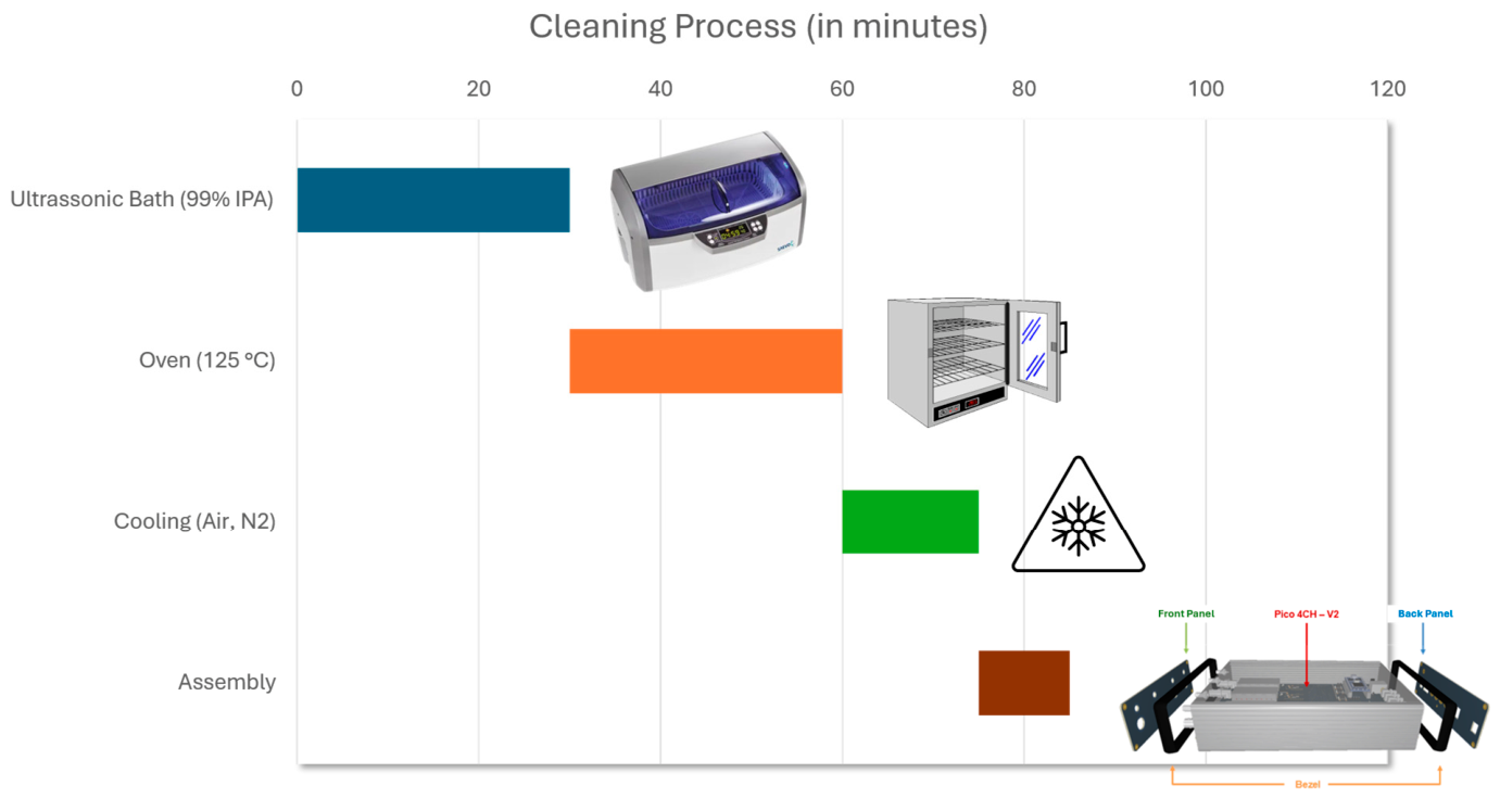
After the soldering process, the mounted PCB must undergo a cleaning cycle to remove residues such as flux, body oils, and absorbed moisture before final assembly. The established cleaning protocol, summarized in Figure 3, is divided into four sequential stages:
  • Ultrasonic bath: immersion for 30 min in an ultrasonic bath using 99% isopropyl alcohol (IPA).
  • Bake-out: placement in a controlled oven environment at 125 °C for 30 min.
  • Cooling: cooling to room temperature, either in ambient air or aided by the flow of dry nitrogen gas.
  • Assembly: final assembly of the device, including the placement of a silica gel packet within the enclosure to manage residual internal humidity.
It is important to note that the duration of the ultrasonic bath and the thermal processing time is empirical and may need adjustment based on the type and the volume of flux residue remaining after soldering. Therefore, the values previously presented should be considered as reference guidelines rather than fixed parameters.
The processing time for each stage was defined using the offset value of the most sensitive range as a figure of merit. Accordingly, instead of relying on predetermined timing values, a more robust approach is to monitor the offset of the most sensitive range, as it effectively captures variations from process-dependent factors.
For TIA amplifiers employing a 10 GΩ feedback resistor (corresponding to a gain of 100 pA/V), the expected offset should remain below 500 μV (or 50 fA) ([11], Section 4).
Humidity presents a major challenge in achieving sub-nanoampere measurement precision by increasing the dielectric constant and enabling surface leakage current within the PCB material. Even with established procedures like extended oven bake-outs or placing electronics in a vacuum chamber, their effectiveness against persistent drift remains inconsistent. For future fabrication batches, planned preventive measures include evaluating alternative PCB materials, such as replacing a standard FR-4 dielectric with a ceramic solution, and exploring the use of non-hygroscopic soldering flux.

2.3. Firmware Architecture

The firmware design is based on the MBED-OS Real-Time Operating System [11] as a strategy for aiding portability to other microcontrollers supported by MBED OS, such as the STM32H7 [16] series from STMicroelectronics, embedded in Caju [15]. Considering the communication thread, two TCP socket servers are provided for different purposes:
  • A configuration socket: ASCII encoded protocol—question- and answer-based.
  • A data streaming socket: unidirectional, from the picoammeter to the host PC. This socket is optimized to transfer all current measurement data packets. This protocol is described in Section 2.3.1.

2.3.1. Data Streaming

The data streaming protocol is binary. Each channel current is expressed as a 32-bit float variable (4 bytes); the channel number is encoded as a byte, and finally, a terminator byte ends the channel data. Fixed-length and terminator words and patterns are crucial for the correct synchronism of binary protocols. START and STOP messages are sent to perform synchronizations in the host application.
The streaming data rate is expressed in Equation (1):
d a t a   r a t e b i t s   p e r   s e c o n d = 48 n c h a n n e l s s a m p l e   r a t e ( s p s )
The maximum data rate can be obtained with all four channels enabled to sample at a 2000 sps rate, resulting in 384 kbps. This data rate is not a real challenge for a 100 Mbps Ethernet link; however, the LPC1768 RAM has only 64 kB for all running tasks, limiting the possibilities for properly buffering this maximum data rate to contend with network oscillations. A thread-safe circular buffer has been implemented to interface acquisition and data streaming threads.
For future improvements, the LPC1768 microcontroller replacement for the STM32H7 should increase any available resources, such as the clock rate, RAM, and DMA features; therefore, a more stable data streaming link is expected under these conditions.

2.3.2. Operating Modes

The quad-channel picoammeter has two operating modes: continuous or triggered, each with its own set of characteristics. It is important to note that each of the four channels can be individually configured to operate in either operating mode. Each channel disposes of its own Finite State Machine (FSM) to control acquisitions and data conversion, as well as push data to the circular buffer.
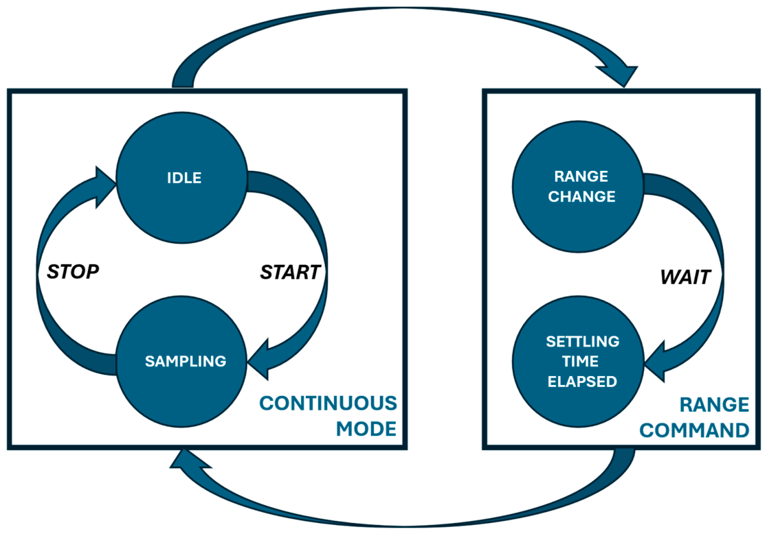
The continuous mode was designed to acquire uninterrupted samples at the required sampling rate. There are only two channel states: SAMPLING or IDLE. There are also two actions (or commands): to START acquisitions or to STOP, as shown in Figure 4:
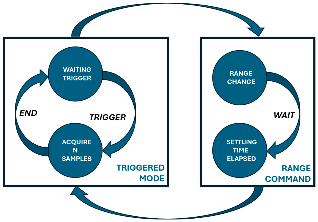
In the triggered mode, as shown in Figure 5, another configuration is the number of samples per trigger pulse, configured by the command socket interface. In this mode, the ADCs are sampled only if the device receives a hardware or software trigger. When the number of samples sent by the ADC reaches the configured number of samples, the sampling process ceases, and then the output trigger changes its logic state. In this condition, the ADC is rearmed and waiting for a new trigger.

2.4. Picolo, the Software Application

Support for the regular use of picoammeters at the LNLS beamlines is provided by an EPICS IOC [20] named “Picolo”, developed by the LNLS/COMP group. This IOC communicates via the EPICS AsynDriver module (v. 4.42), a framework for asynchronous device communication [21], using the command set defined by the picoammeter’s firmware.
To maximize performance and avoid data loss, the firmware was redesigned to support two simultaneous Ethernet connections: one TCP/IP port dedicated to command and response handling, and the other exclusively for data transfer. Accordingly, the IOC employs a separate thread for each connection to efficiently distribute CPU workload. A third thread is dedicated to handling data file writing (on demand), as the IOC can be configured to write acquired data directly to file in parallel with acquisition.
For user convenience, offset and gain adjustments are provided for each channel, computed as angular and linear coefficients, which are all configurable via Process Variables (PVs). In triggered mode, the acquisition time and the number of data points are set. The acquired data are buffered in memory and made available by the IOC, along with a timestamp. As a safeguard against accidental data loss, the data buffer reset operation is only permitted when the picoammeter is neither acquiring nor in trigger mode.
The PVs exposed by “Picolo” are loaded from two main database definition files. One defines PVs related to the overall device (e.g., file parameters, device name, serial number, firmware, and IOC versions); the other defines PVs associated with individual channels. PV naming follows the Sirius beamlines convention with two patterns, beamline:hutch:system:function and beamline:hutch:system:channel:function, resulting in PVs that represent the device location, as in SPU:B:PICO01:Firmware and SPU:B:PICO02:Current1:ScaleFactor_RBV.
The IOC runs within a containerized environment standardized across the Sirius beamlines, the epics-in-docker framework [22].

3. Results

3.1. Characterization and Data Analysis

In this subsection, further details about the characterization and data analysis of two figures of merit that are positively correlated, the bandwidth and the RMS noise, are provided. Moreover, as every picoammeter channel is characterized across all eight transimpedance scales, the statistical analysis of these metrics is also presented.

3.1.1. Bandwidth

The bandwidth characterization procedure begins with injecting a sinusoidal current sweep from the Keithley 6221 current source (Tektronix, Beaverton, OR, USA) [23]. To ensure measurement accuracy across the frequency range, the sine wave amplitude was set to 90% of the full scale of the selected range, and data were acquired over a minimum of three complete periods for each tested frequency. The measurement data pair, consisting of the frequency and the normalized peak-to-peak amplitude, was stored. This procedure was performed on every channel and each transimpedance scale using the 2000 SPS sampling frequency.
To estimate the total continuous frequency response function and, consequently, the cutoff frequency for each of the ten selectable sampling rates, a curve-fitting algorithm was employed. The algorithm was developed based on the premise that all cascaded filters in the signal path are independent. Hence, the total filter response in the frequency domain is the multiplication of the individual transfer functions of each filtering stage, as shown in Equation (2).
H T o t a l f = H T r a n s i m p e d a n c e f   H P r e A D C f   H A D C f
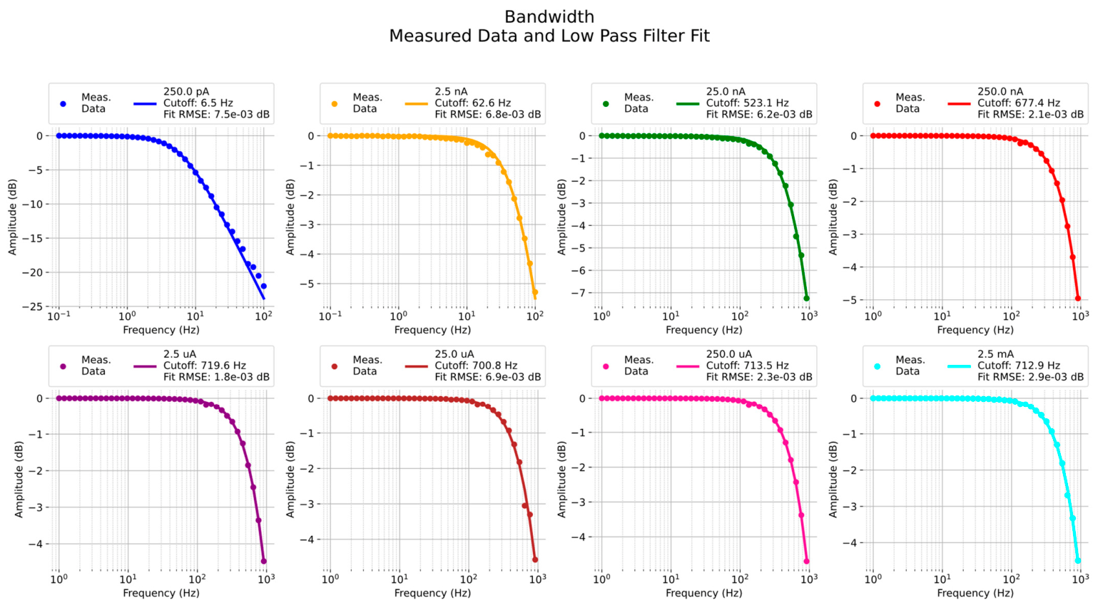
The algorithm uses the measured data (the pair frequency and the normalized amplitude) acquired at 2000 SPS to fit a theoretical continuous function based on the expected first-order low-pass transfer function for each stage. These estimated cutoff frequencies are then used to predict the overall bandwidth at all other lower sampling rates. Figure 6 shows the measured data and the resulting continuous curve fitting of the frequency response for each transimpedance scale at 2000 SPS. Figure 6 also highlights the associated cutoff frequencies and the root mean squared error (RMSE) of the curve fitting for each case.

3.1.2. RMS Noise

To evaluate the intrinsic noise of the picoammeter [10,11,12], the current input connector of each channel is terminated with a shielded open cap. The acquisition parameters are set to the maximum sampling frequency of 2000 SPS, and 40,000 samples are acquired per scale and per channel. The acquired time-domain samples are then processed using Welch’s method [24,25] to compute the Noise Spectral Density (NSD).
Using the measured NSD ( i n d e n R M S ) reported in [11] and obtained from a null-input, shielded cap setup under standard ambient conditions (20 °C), together with the system bandwidth (defined by the cutoff frequency ( f c ) determined in Section 3.1.1) the total integrated RMS current noise is calculated for each combination of transimpedance gain setting and ADC sampling frequency. This calculation is performed by integrating the NSD over the effective system bandwidth, as described in Equation (3). The minimum frequency ( f m i n ) achievable using Welch’s method falls within the sub-hertz range for this setup, based on acquisition times of 30 s.
i n R M S = f m i n f c i n d e n R M S 2 d f
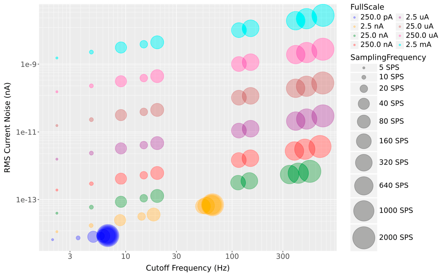
The average values of the cutoff frequency and RMS current noise for each scale and sampling frequency are summarized graphically in Figure 7.

3.1.3. Statistical Evaluation

As a large dataset of measurements (hundreds of trials) was performed across all channels and scales, it was possible to statistically evaluate the performance of the curve-fitting algorithm and the consistency of the RMS noise calculation. This was achieved through the calculation of the coefficient of variation (CV), which assesses the dispersion of the data relative to the mean value. The CV is the ratio between the standard deviation (σ) and the mean (μ) value, as shown in Equation (4).
C V = σ μ
The calculated average, standard deviation, and coefficient variation values of the cutoff frequency and RMS current noise are described in Table 2 and Table 3, respectively.
The maximum coefficient of variation for the cutoff frequency is 7% (Table 2), indicating considerably low variability across the dataset. These results support the conclusion that the employed algorithm for determining the frequency response is robust and adequate for each scale and sampling frequency. The highest CV values are observed in the 250 pA scale, particularly at lower cutoff frequencies. This increased variation is likely attributed to the lower number of data points acquired in this specific region during the characterization process.
When evaluating the RMS current noise (Table 3), the CV remains consistently low (<20%) for the majority of scale and sampling frequency combinations. The notable exception is observed at the 250 pA scale with a 5 SPS sampling rate. This most sensitive measurement range is inherently more susceptible to undesirable influences, such as cabling triboelectric effects, mechanical vibrations, and electromagnetic interference (EMI).
This particular configuration poses a similar characterization challenge to that encountered during bandwidth evaluation, where a significantly reduced number of data points was available compared to other configurations. Consequently, statistical robustness is somewhat compromised under these conditions.
Overall, the results demonstrate the effectiveness and reliability of the RMS current noise calculation methodology across the instrument’s operational range. Nevertheless, future characterization efforts will include the use of a fully shielded EMI chamber to improve experimental conditions—particularly for the 250 pA range—enhancing the accuracy of both noise and bandwidth measurements.

3.2. Triggered Mode: Time and Frequency Analyses

This subsection is dedicated to analyzing the latency and time requirements during the triggered acquisition process and establishing the critical relationship between the acquisition speed and the front-end bandwidth.

3.2.1. The Acquisition Process and Timing Model

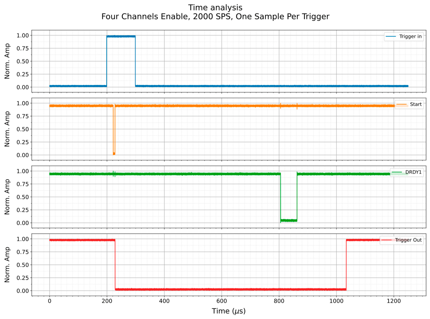
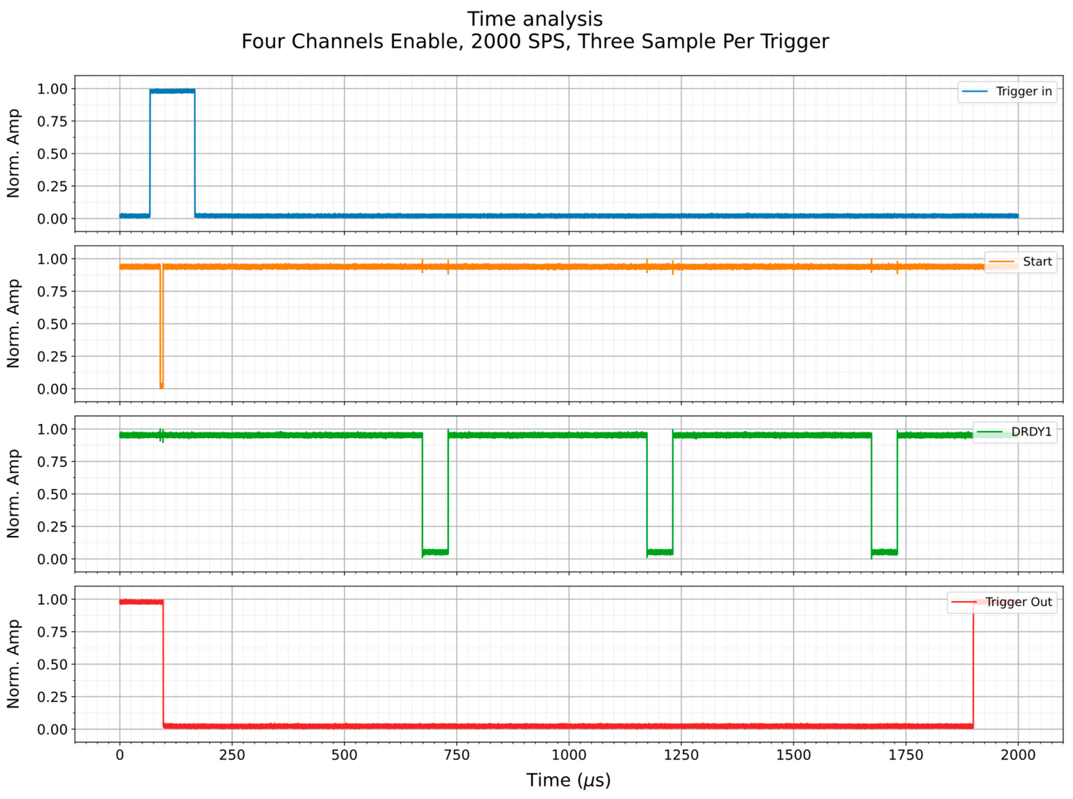
The analysis of the acquisition timing is defined by the interval between the input trigger’s rising edge and the resultant output trigger’s rising edge. For this evaluation, four signals must be considered: the input trigger, the ADC start and data-ready pins, and the output trigger.
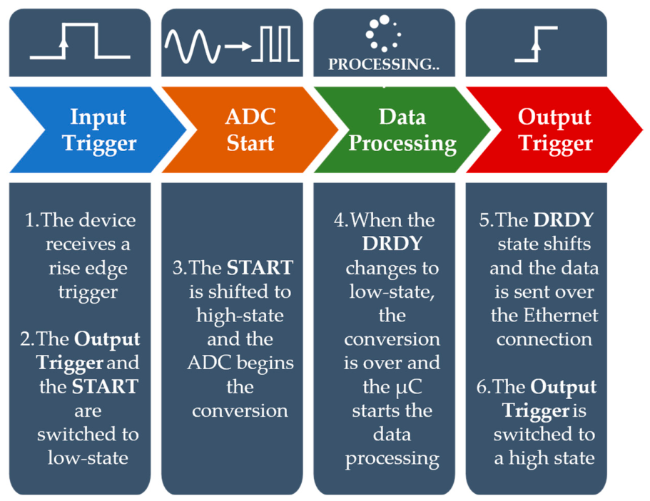
Figure 8 shows a typical time diagram of the trigger acquisition mode when the number of samples per trigger is set to one. The detailed explanation of the state change meaning is shown in Figure 9.
A similar analysis can be performed when the picoammeter is configured to provide multiple samples for each trigger signal. In this configuration, the ADC is set up to deliver the specified number of samples, and only the data-ready pin transitions after the first conversion are relevant until the required sample count is reached. It is important to note that the first conversion time is longer than subsequent ones, as described in the ADC datasheet [13], and is more susceptible to timing variations (jitter).
The total time equation for the triggering process with one sample (Equation (5)) and multiple samples (Equation (6)) can be inferred from the time diagrams in Figure 8 and Figure 10, respectively. The description of each argument of Equations (5) and (6) is presented in Table 4.
t t o t = t s c d + t A D C + t µ C + t e t h
t t o t = t s c d + t A D C + N 1 t s m p s + t µ C + t e t h
An important characteristic in this operating mode is that the device firmware disregards any additional input trigger signal while the current acquisition process is incomplete. Due to this constraint, the maximum allowable trigger frequency ( f t r g m a x ) can be calculated using the total acquisition time in triggered mode (Equations (5) and (6)), as shown in Equation (7).
f t r g m a x = 1 t t o t .

3.2.2. Time Measurements

The time measurements were experimentally obtained using the Keysight 33220A waveform generator (Keysight Technologies, Santa Rosa, CA, USA) [26] to produce the trigger signals and the Keysight DSOS104A digital oscilloscope (Keysight Technologies, Santa Rosa, CA, USA) [27] to gather the time interval between the edges.
Table 5 presents the measured time intervals for the individual components of the acquisition process. It is observed that the parameters requiring direct microcontroller intervention (tscd, tµC, teth) exhibit a higher jitter compared to the ADC-specific parameters (tADC, tsmps). This discrepancy exemplifies the non-deterministic nature of the microcontroller’s response, stemming from the concurrent management of the data stream and various picoammeter peripherals. It is anticipated that the transition to a more powerful microcontroller (as discussed in Section 2.1.4) will significantly reduce this variation and improve timing determinism.
The total measured time intervals for two distinct experimental configurations are summarized in Table 6. The total measured time interval and jitter for one and three samples per trigger pulse are as follows:
  • Single-sample mode: 2000 SPS, four channels enabled, one sample per trigger pulse (Figure 8).
  • Multi-sample mode: 2000 SPS, four channels enabled, three samples per trigger pulse (Figure 10).
In both configurations, 3000 trigger cycles were acquired to facilitate a fair jitter evaluation. A direct comparison reveals that while the total standard deviation remains comparable in both scenarios, the standard deviation per sample is considerably higher in the first configuration. By extrapolating this result to a much larger number of samples, the total standard deviation is expected to remain relatively constant, whereas the standard deviation per sample would decrease significantly.
These observations corroborate the hypothesis that multi-sample acquisition (as described in Section 3.2.1) provides greater immunity against timing imprecision (jitter), resulting in more stable and deterministic timing performance. Since tscd, tµC, and teth are independent of the ADC sampling rate, and tADC can be extracted from the manufacturer’s lookup table [13]. These experimental results allow for an accurate estimation of the total conversion time and, consequently, the maximum trigger frequency for every available ADC sampling rate.
Table 7 summarizes the values of the conversion time (Tconv), the maximum trigger frequency ( f t r g m a x ), and signal bandwidth (BWsig). Equation (6) has been used to estimate the maximum trigger frequency, taking into consideration that the standard deviation of tADC was neglected due to its deterministic characteristic, and the total employed time was defined as the mean value plus three times the standard deviation to establish a robust timing margin. The signal bandwidth was calculated using Equation (8).
B W s i g = f t r g m a x 2
When comparing the system cutoff frequencies from Table 2 to the digital signal bandwidth (BWsig) values from Table 7, it is noticed that the cutoff frequencies for the combination of scales and sampling rates are greater than the BWsig values. This finding indicates that the analog front-end bandwidth is over-designed and can be optimized (i.e., reduced) in future revisions to minimize the RMS current noise.
On the other hand, if the application requires higher digital bandwidths to read faster input signals, the entire acquisition chain would require modification. This necessitates not only replacing the existing ADC with a component featuring higher sampling frequencies but also upgrading the microcontroller with greater processing capacity. This is essential because the current microcontroller’s processing time is already in the same order of magnitude as the ADC conversion time (Table 5), effectively forming a data throughput bottleneck that limits the maximum sustainable trigger rate and digital bandwidth.

3.3. Application at Sirius’ Beamlines

The high-resolution quad-channel picoammeter has been successfully integrated and commissioned across several experimental stations at Sirius. The following subsections detail the instrument’s performance in three distinct high-demand scenarios: synchronous on-the-fly energy scanning for absorption spectroscopy, synchronous transmitted beam intensity for data normalization for scattering measurements, and high-speed beam position monitoring. These applications demonstrate the device’s capability to provide critical diagnostic data under real-world machine operation conditions.

3.3.1. Measurement at SABIA Beamline

At the SABIA (Soft x-ray ABsorption spectroscopy and ImAging) beamline [28], the quad-channel picoammeter is essential for conducting absorption measurements. The first channel is connected to a gold mesh to measure the beam intensity (I0), and the second channel is directly connected to the sample to measure the transmitted or absorbed current (I1). The ratio between the I1 and I0 is the sample absorption amount.
To generate X-ray absorption spectra, the experiments use the on-the-fly scanning technique that moves the optical elements (undulator, monochromator, and mirrors) to provide energy scanning and perform current measurements synchronously. The synchronization is managed by the LNLS Timing and Trigger Unit (TATU) [29]. Depending on the experimental requirements, the number of samples and input trigger pulses can range from hundreds to tens of thousands per scan.
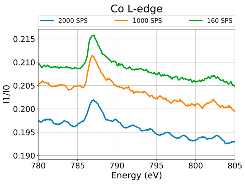
Figure 11 illustrates a practical application where the signal-to-noise ratio (SNR) is critical, such as when evaluating materials with low electron mobility that produce noisy current signals. In such cases, the user can adjust the ADC sampling rate to optimize the SNR. As observed in the Cobalt (Co) L-edge absorption spectrum (Figure 11), lower sampling frequencies (e.g., 160 SPS) result in a smoother spectrum compared to higher rates (e.g., 2000 SPS) for the same acquisition time. This improvement is directly supported by the statistical data in Table 3, which shows that reducing the sampling frequency leads to lower RMS current noise across all transimpedance scales. These experimental results confirm that the picoammeter’s flexible sampling configurations allow researchers to effectively balance measurement bandwidth against the required resolution for sensitive beamline applications.

3.3.2. Measurement at SAPUCAIA Beamline

At the SAPUCAIA (Scattering APparatUs for Complex Applications and in situ Assays) beamline [30], the quad-channel picoammeter measures the transmitted beam intensity, where real-time monitoring of the transmitted intensity is required in SAXS (small-angle X-ray scattering) experiments for data normalization. Fast acquisition of the transmitted intensity is also required for time-resolved measurements. A second picoammeter device also monitors the incident beam intensity for beam stability diagnostics, ensuring reliable SAXS experiments.
The SAXS measurement consists of synchronized acquisition of the area detector image and the transmitted beam intensity from the quad-channel picoammeter, managed by the LNLS Timing and Trigger Unit (TATU) [29]. A typical measurement involves the acquisition of multiple images, with exposure times ranging from milliseconds to several seconds. The data are then normalized to the transmitted beam intensity to compensate for sample absorption and solvent background contributions.
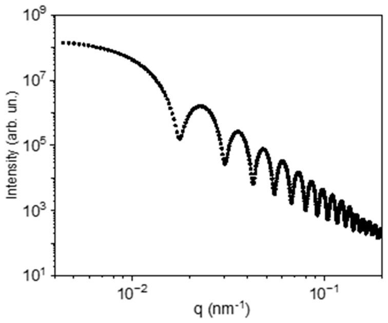
Figure 12 represents a SAXS profile of 500 nm silica nanoparticles, normalized using real-time measurements of the transmitted beam intensity from the quad-channel picoammeter. The area detector image was collected with an exposure time of 1 s, while the transmitted intensity was recorded using the quad-channel picoammeter at an acquisition rate of 1 kHz, sampling the response of a silicon photodiode, which was averaged and used for normalization of the SAXS data.

3.3.3. Measurement at MANACÁ Beamline

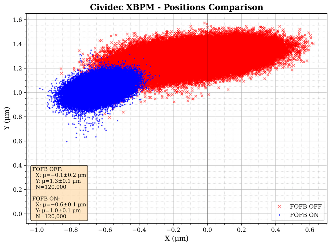
At the MANACÁ beamline [31], the quad-channel picoammeter is used for beam diagnostics using CVD diamond X-ray Beam Position Monitor (XBPM; CIVIDEC Instrumentation GmbH, Vienna, Austria). The device measures current signals from a four-quadrant photodiode, allowing the determination of horizontal and vertical beam positions, which are essential for beam alignment control. In addition, the sum of the channel currents is used to evaluate the photon flux, enabling a continuous assessment of beam intensity [32].
To evaluate the impact of the Fast Orbit Feedback (FOFB) system on beam position stability, tests were carried out under controlled machine conditions, with the FOFB disabled and enabled [33]. The XBPM was previously aligned as close as possible to the beam center, which was defined as the origin of the coordinate system. The quad-channel picoammeter was used to acquire the currents from each photodiode segment of the XBPM.
Figure 13 shows a comparison of the beam position measured by the XBPM with the Fast Orbit Feedback (FOFB) system disabled and enabled. The data correspond to 120,000 samples acquired at a sampling rate of 2000 SPS. With the FOFB enabled, a significant reduction in beam centroid fluctuations is observed. In the horizontal axis, the standard deviation decreases from 0.22 μm to 0.08 μm, corresponding to a reduction of approximately 64%. In the vertical axis, the standard deviation is reduced from 0.08 μm to 0.06 μm, representing an improvement of about 24%. These results demonstrate the effectiveness of the FOFB system in improving beam stability at the MANACÁ beamline.

4. Discussion

The characterization and experimental results presented in this work confirm that the quad-channel picoammeter meets the stringent requirements for low-current diagnostics at the Sirius light source. However, the analysis also reveals critical pathways for future development to enhance instrument performance and reliability.
The finding that the analog front-end bandwidth significantly exceeds the digital signal bandwidth suggests that the current hardware is over-designed for its present sampling rates. This implies a clear opportunity for optimization: by reducing the analog bandwidth in future hardware revisions, the RMS current noise can be further minimized, directly improving the signal-to-noise ratio (SNR) for ultra-low current applications. Furthermore, the transition from the NXP LPC1768 to the STM32H7-based “Caju” platform is essential to overcome the current limitations in RAM capacity and I/O availability.
Future work will focus on implementing these robust buffering strategies and optimizing the interplay between the microcontroller processing time and Ethernet communication to ensure data integrity during “on-the-fly” scanning experiments. The significantly higher processing capacity and expanded memory of the new “Caju” microcontroller are expected to improve capabilities by providing more efficient interruption handling and larger data buffers. These improvements will solidify the picoammeter’s role as a high-reliability component within the broader Sirius control system infrastructure.

5. Conclusions

The commissioning of the quad-channel picoammeter across multiple Sirius beamlines has necessitated a rigorous investigation into the system’s bandwidth characterization and the timing constraints inherent to the triggered acquisition mode. The curve-fitting algorithm that was utilized to model the frequency response for each transimpedance scale and sampling rate combination was validated by statistical analysis, with a coefficient of variation consistently below 7%. Conversely, while the RMS current noise calculation serves as a reliable performance guide for most configurations, higher variation coefficients in specific low-current ranges—such as the 250 pA scale at 5 SPS—indicate areas for further algorithmic refinement and outlier tracking.
Future plans include the implementation of an EMI-shielded chamber to enhance the robustness of measurements, particularly for the most sensitive range characterization. This controlled environment will be essential to minimize interference from external electromagnetic sources, ensuring greater reliability during long-term measurement campaigns. Additionally, further studies will be conducted to evaluate calibration deviations over extended periods of usage, allowing for a more accurate assessment of system stability and performance over time.
Detailed timing analysis in triggered mode enabled the estimation of acquisition latencies, establishing definitive maximum trigger frequencies and digital signal bandwidths. A comparison between these results and the characterized analog cutoff frequencies suggests that the front-end bandwidth is currently over-designed, providing a clear pathway for noise reduction in future hardware iterations. The transition to a higher-performance microcontroller platform was identified as a primary solution to ensure absolute data integrity and avoid occasional data losses at the highest sample rate of 2 ksps with all four channels enabled.
Finally, the successful implementation of on-the-fly scanning at the SABIA beamline, as well as the SAXS measurement at the SAPUCAIA beamline, and the high-resolution beam position monitoring at the MANACÁ beamline, validates the reliability, precision, and repeatability of the instrument for complex synchrotron applications.

Author Contributions

Conceptualization, L.Y.T., M.M.D. and F.H.C.; Data curation, L.Y.T., A.R.P. and V.S.O.; Formal analysis, L.Y.T. and M.M.D.; Funding acquisition, F.H.C.; Investigation, L.Y.T. and M.M.D.; Methodology, L.Y.T. and M.M.D.; Project administration, F.H.C. and P.H.N.; Software, M.M.D., V.S.O. and J.R.P.; Supervision, M.M.D., F.H.C. and P.H.N.; Validation, L.Y.T.; Writing—original draft, L.Y.T., V.S.O., A.R.P. and J.R.P.; Writing—review and editing, L.Y.T., M.M.D. and P.H.N. All authors have read and agreed to the published version of the manuscript.

Funding

This research was funded by the Brazilian Ministry of Science, Technology, and Innovation, and the APC was funded by the MDPI Instruments Editorial Office as an invitation to prepare an extended version of the IBIC 2024 proceedings paper entitled “High-resolution quad-channel picoammeter: characterization and commissioning”.

Data Availability Statement

The picoammeter hardware design is openly available at CERN’s Open Hardware repository at https://gitlab.com/ohwr/project/P4CH-LNLS (accessed on 2 June 2026) [17]. The results of this article were obtained using the version tagged as V2.1. The picoammeter characterization raw data will be made available by the authors upon request. The results of this article have been obtained using the version tagged as V2.1. The picoammeter characterization raw data will be made available by the authors on request.

Acknowledgments

The authors gratefully acknowledge the financial support received from the Brazilian Ministry of Science and Technology, and Innovation as well as the contributions of the LNLS teams, particularly the Software Controls Group, for the IOC development. The authors also thank all beamlines involved in this project, with special recognition to the SAPUCAIA, MANACA, and SABIA beamlines for providing the scientific results presented in this work.

Conflicts of Interest

The authors declare no conflicts of interest. The funders had no role in the design of the study; in the collection, analyses, or interpretation of data; in the writing of the manuscript; or in the decision to publish the results.

References

  1. Liu, L.; Resende, X.R.; de Sá, F.H. A New Optics for Sirius. In Proceedings of the 7th International Particle Accelerator Conference (IPAC’16), Busan, Republic of Korea, 8–13 May 2016; pp. 3413–3416. [Google Scholar]
  2. Nida, S.; Tsibizov, A.; Ziemann, T.; Woerle, J.; Moesch, A.; Schulze-Briese, C.; Pradervand, C.; Tudisco, S.; Sigg, H.; Bunk, O.; et al. Silicon carbide X-ray beam position monitors for synchrotron applications. J. Synchrotron Radiat. 2019, 26, 28–35. [Google Scholar] [CrossRef] [PubMed]
  3. CAEN ELS. AH501D: 4-Channel Bipolar Picoammeter with Analog Monitors and Bias Voltage. Available online: https://www.caenels.com/product/ah501d/ (accessed on 2 June 2026).
  4. CAEN ELS. AH401D: 4-Channel Charge Integration Picoammeter. Available online: https://www.caenels.com/product/ah401d/ (accessed on 2 June 2026).
  5. Texas Instruments. DDC114: Quad Current Input 20-Bit Analog-to-Digital Converter. Available online: https://www.ti.com/product/DDC114 (accessed on 2 June 2026).
  6. Sydor Technologies. SI-EP-B4 4 Channel Electrometer Preliminary Specifications. Available online: https://sydortechnologies.com/files/Data-Sheet-SI-EP-B4.pdf (accessed on 2 June 2026).
  7. Siddons, D.P. Operating Manual for the NSLS-II X-Ray BPM Module; Brookhaven National Laboratory: Upton, NY, USA. Available online: https://wiki-nsls2.bnl.gov/beamline17BM/upload/2/24/NSLS2_EM_manual.pdf (accessed on 2 June 2026).
  8. Avila-Abellan, J.; Broseta, M.; Cuni, G.; Matilla, O.; Rodriguez, M.; Ruz, A.; Salabert, J.; Serra-Gallifa, X.; ALBA-CELLS Synchrotron; Milan-Otero, A.; et al. Em# Electrometer Comes to Light. In Proceedings of the 16th International Conference on Accelerator and Large Experimental Physics Control Systems, Barcelona, Spain, 8–13 October 2017. [Google Scholar]
  9. Lidón-Simon, J.; Fernandez-Carreiras, D.; Gigante, J.-V.; Jan Jamroz, J.; Klora, J.; Matilla, O.; CELLS-ALBA Synchrotron. Low Current Measurements at ALBA. In Proceedings of the ICALEPCS2011, WEPMS025, Grenoble, France, 10–14 October 2011. [Google Scholar]
  10. Tanio, L.; Cardoso, F.; Donatti, M. High-resolution quad-channel picoammeter: Characterization and commissioning. In Proceedings of the IBIC2024, Beijing, China, 9–13 September 2024; pp. 426–430. [Google Scholar] [CrossRef]
  11. Donatti, M.M.; Cardoso, F.H.; Tanio, L.Y. Development of a quad-channel high-resolution digital picoammeter for beam diagnostics. IEEE Open J. Instrum. Meas. 2024, 19, C03028. [Google Scholar] [CrossRef]
  12. Tanio, L.Y.; Cardoso, F.H.; Donatti, M.M. A Multirange Low Noise Transimpedance Amplifier for Sirius Beamlines. In Proceedings of the 12th International Particle Accelerator Conference (IPAC’21), Campinas, Brazil, 24–28 May 2021; pp. 3447–3450. [Google Scholar] [CrossRef]
  13. Texas Instruments. ADS1246: 24-Bit Analog-to-Digital Converter (ADC) for Low-Noise Sensor Measurement, ADS1246 Datasheet, September 2011 [Revised January 2022]; Texas Instruments: Dallas, TX, USA, 2011. [Google Scholar]
  14. NXP. Arm LPC1768 Board. Available online: https://www.nxp.com/products/processors-and-microcontrollers/arm-microcontrol-lers/general-purpose-mcus/lpc1700-cortex-m3/arm-mbed-lpc1768-board:OM11043 (accessed on 15 November 2025).
  15. CAJU Module. Open Hardware Repository. Available online: https://www.gitlab.com/ohwr/project/caju-module (accessed on 12 December 2025).
  16. STMicroelectronics. STMH7 Series. Available online: https://www.st.com/en/microcontrollers-microprocessors/stm32h7-series.html (accessed on 15 November 2025).
  17. Quad-Channel Digital Pico Ammeter Open Hardware Repository. Available online: https://gitlab.com/ohwr/project/P4CH-LNLS (accessed on 5 March 2026).
  18. Keithley Instruments. Low Current Measurements. In Low Level Measurements Handbook—Precision DC Current, Voltage and Resistance Measurements, 7th ed.; Keithley Instruments: Solon, OH, USA, 2014; pp. 2–15–2–39. [Google Scholar]
  19. Analog Devices. High Impedance Measurements. In Data Sheet ADA4530-1, Femtoampere Input Bias Current Electrometer Amplifier, Rev. C; Analog Devices: Singapore, 2024; pp. 32–39. [Google Scholar]
  20. Experimental Physics and Industrial Control System (EPICS). EPICS Base Documentation, Release 7.0.7, Argonne National Laboratory. Available online: https://epics.anl.gov/base/R7-0/7.php (accessed on 12 December 2025).
  21. Johnson, M.R. AsynDriver: Asynchronous Driver Support for EPICS. Available online: https://epics.anl.gov/modules/soft/asyn/R4-29/asynDriver.html (accessed on 12 December 2025).
  22. Nogueira Rolim, É.; Rodrigues de Lima, G.; de Souza dos Reis, G.; da Fonseca Simões, H. epics-in-docker: A small framework for building slim IOC and EPICS tooling container images. In Proceedings of the 20th International Conference on Accelerator and Large Experimental Physics Control Systems (ICALEPCS’25), Chicago, IL, USA, 20–26 September 2025; JACoW Publishing: Geneva, Switzerland, 2025; pp. 1096–1102. [Google Scholar] [CrossRef]
  23. Keithley. Model 6220 DC Current Source, Model 6221 AC and DC Current Source, Users Manual, Rev. C; Keithley: Ohio, UK, 2008. [Google Scholar]
  24. Solomon, O.M., Jr. PSD Computations Using Welch’s Method; Sandia Report 1991, SAND91–1533; Sandia National Laboratories: Albuquerque, NM, USA, 1991. [Google Scholar]
  25. Same, M.H.; Gandubert, G.; Gleeton, G.; Ivanov, P.; Landry, R., Jr. Simplified Welch Algorithm for Spectrum Monitoring. Appl. Sci. 2021, 11, 86. [Google Scholar] [CrossRef]
  26. Keysight Technologies. Keysight 33220A 20 MHz Function/Arbitrary Waveform Generator; Keysight Technologies: Santa Clara, CA, USA, 2015. [Google Scholar]
  27. Keysight Technologies. Infiniium S-Series: The Standard for Superior Measurements; Keysight Technologies: Santa Clara, CA, USA, 2022. [Google Scholar]
  28. Zilli, V.B.; Basilio, G.G.; Cezar, J.C.; Del Nero, F.A.; Ferreira, G.R.B.; Francisco, B.A.; Gardingo, M.E.O.A.; Geraldes, R.R.; Pinto, A.C.; Rodrigues, G.L.M.P.; et al. Exactly Constrained, High Heat Load Design for SABIA’s First Mirror. In Proceedings of the 12th International Conference on Mechanical Engineering Design of Synchrotron Radiation Equipment and Instrumentation, (MEDSI2023), Beijing, China, 6–10 November 2023; pp. 44–47. [Google Scholar]
  29. Piton, J.R.; Alnajjar, D.; Araujo, D.H.C.; Brito Neto, J.L.; do Carmo, L.P.; Guedes, L.C.; de Moraes, M.A.L. TATU: A Flexible FPGA-Based Trigger and Timer Unit Created on CompactRIO for the First Sirius Beamlines. In Proceedings of the 18th International Conference on Accelerator and Large Experimental Physics Control Systems (ICALEPCS’21), Shanghai, China, 18–22 October 2021; pp. 908–911. [Google Scholar]
  30. Rigamonti, H., Jr.; de Albuquerque, G.S.; Candido, L.B.; Meyer, B.C.; Silva, M.S.; Zilli, V.B.; Barbosa, L.R.S. Optical design and preliminary commissioning results with a temporary undulator of the Sirius’ SAXS beamline SAPUCAIA. J. Phys. Conf. Ser. 2025, 3010, 012061. [Google Scholar] [CrossRef]
  31. Nascimento, A.; Araujo, E.; Hagio, C.; Almeida, S.; Rodrigues, A.C.; Trivella, D.B.B.; Bruder, M.; Rustiguel, J.K.; Ropke, C.D.; Pessa, L.R.; et al. Launch of the Manacá Beamline at Sirius: First Protein Crystallography Structures and New Opportunities for Pharmaceutical Development Using Synchrotrons. Synchrotron Radiat. News 2021, 34, 3–10. [Google Scholar] [CrossRef]
  32. Melbinger, J.; Fragner, T.; Griesmayer, E.; Kalbfleisch, S.; Frais-Kölbl, H.; Weiss, C. Diamond XBPM® for feedback control of the X-ray beam position. J. Phys. Conf. Ser. 2025, 3010, 012075. [Google Scholar] [CrossRef]
  33. Tavares, D.O.; Aguiar, M.S.; Cardoso, F.H.; Coelho, E.P.; Cruz, G.R.; de Sá, F.H.; Giachero, A.F.; Lin, L.; Marques, S.R.; Oliveira, A.C.S.; et al. Commissioning and Optimization of the SIRIUS Fast Orbit Feedback. In Proceedings of the 19th International Conference on Accelerator and Large Experimental Physics Control Systems (ICALEPCS 2023), Cape Town, South Africa, 9–13 October 2023. [Google Scholar] [CrossRef]
Figure 1. Simplified block diagram of the quad-channel picoammeter. Arrows show the direction of signal propagation.
Instruments 10 00032 g001
Figure 2. Block diagram of the analog front-end circuit.
Instruments 10 00032 g002
Figure 3. The amount of time (in minutes) for each step of the cleaning process until the device’s assembly.
Instruments 10 00032 g003
Figure 4. Continuous mode FSM (Finite State Machine). Arrows indicate FSM transitions after a range change command is received.
Instruments 10 00032 g004
Figure 5. Triggered mode FSM (Finite State Machine). Arrows indicate FSM transitions after a range change command is received.
Instruments 10 00032 g005
Figure 6. Frequency response at 2000 SPS. Measured data and low-pass filter fit.
Instruments 10 00032 g006
Figure 7. RMS noise current vs. cutoff frequency for each scale and sampling frequency. The numerical results are summarized in Table 2 and Table 3.
Instruments 10 00032 g007
Figure 8. Time diagram in trigger acquisition mode at 2000 SPS and one sample per trigger.
Instruments 10 00032 g008
Figure 9. Step-by-step of triggering the acquisition process.
Instruments 10 00032 g009
Figure 10. Time diagram in trigger acquisition mode at 2000 SPS and three samples per trigger.
Instruments 10 00032 g010
Figure 11. Cobalt (Co) L-edge absorption spectrum for different ADC sampling frequencies (160, 1000, and 2000 SPS) and the same acquisition time.
Instruments 10 00032 g011
Figure 12. SAXS profile of 500 nm silica nanoparticles, normalized using real-time measurements of the transmitted beam intensity from the quad-channel picoammeter.
Instruments 10 00032 g012
Figure 13. Beam centroid position measured by the Cividec CVD diamond XBPM at the MANACÁ beamline with the Fast Orbit Feedback (FOFB) system disabled (red crosses) and enabled (blue dots).
Instruments 10 00032 g013
Table 1. Transimpedance amplifier theoretical characteristics: full-scale, sensitivity, and bandwidth.
ScaleFull ScaleSensitivityBandwidth
1250 pA100 pA/V16 Hz
22.5 nA1 nA/V154 Hz
325 nA10 nA/V711 Hz
4250 nA100 nA/V711 Hz
52.5 µA1 µA/V711 Hz
625 µA10 µA/V711 Hz
7250 µA100 µA/V711 Hz
82.5 mA1 mA/V711 Hz
Table 2. Average (µ), standard deviation (σ), and coefficient variation (CV) values of the cutoff frequency (Hz) for each scale and sampling frequency.
Fs
(SPS)
250 pA2.5 nA25 nA250 nA
μσCVμσCVμσCVμσCV
52.060.020.012.260.00*2.260.00*2.260.00*
103.580.100.034.740.001.05 × 10−34.760.00*4.760.00*
205.810.330.0614.120.064.07 × 10−314.790.00*14.790.013.38 × 10−4
404.970.220.048.860.021.70 × 10−39.030.00*9.030.00*
806.670.380.0618.300.126.46 × 10−319.780.001.05 × 10−419.790.001.29 × 10−4
1606.790.500.0753.221.753.28 × 10−2113.870.383.31 × 10−3115.510.383.28 × 10−3
3206.800.500.0757.002.083.65 × 10−2145.300.765.23 × 10−3148.650.795.34 × 10−3
6406.800.500.0764.362.904.50 × 10−2346.688.142.36 × 10−2385.1111.212.91 × 10−2
10006.800.500.0764.952.984.58 × 10−2418.5013.413.20 × 10−2482.1720.034.15 × 10−2
20006.810.500.0765.473.044.65 × 10−2537.6018.083.36 × 10−2670.0217.862.67 × 10−2
Fs
(SPS)
2.5 μA25 μA250 μA2.5 mA
μσCVμσCVμσCVμσCV
52.260.00*2.260.00*2.260.00*2.260.00*
104.760.00*4.760.00*4.760.00*4.760.00*
2014.800.003.00 × 10−414.800.003.16 × 10−414.800.003.16 × 10−414.800.003.16 × 10−4
409.030.00*9.030.00*9.030.00*9.030.00*
8019.790.00*19.790.00*19.790.00*19.790.00*
160115.870.312.70 × 10−3115.850.342.93 × 10−3115.880.342.91 × 10−3115.850.353.03 × 10−3
320149.410.664.40 × 10−3149.360.714.78 × 10−3149.420.714.75 × 10−3149.360.744.96 × 10−3
640395.929.932.51 × 10−2395.2210.802.73 × 10−2396.1210.722.71 × 10−2395.3011.262.85 × 10−2
1000501.5618.243.64 × 10−2500.3219.863.97 × 10−2501.9119.703.92 × 10−2500.4720.784.15 × 10−2
2000713.9720.042.81 × 10−2711.8920.352.86 × 10−2713.5122.553.16 × 10−2715.6722.193.10 × 10−2
* For coefficient of variation (CV) values below 1 × 10⁻⁴, the standard deviation is negligible and does not provide meaningful information for variation analysis.
Table 3. Average (µ), standard deviation (σ), and coefficient variation (CV) values of the RMS current noise (A) for each scale and sampling frequency.
Fs
(SPS)
250 pA2.5 nA25 nA250 nA
μ (×10−15)σ (×10−16)CVμ (×10−14)σ (×10−15)CVμ (×10−13)σ (×10−14)CVμ (×10−12)σ (×10−14)CV
52.576.110.240.580.510.090.200.170.080.131.480.11
103.015.300.180.870.470.050.320.200.060.201.530.08
203.514.610.131.560.550.030.580.220.030.371.650.04
403.344.720.141.210.500.050.460.200.040.291.690.06
803.594.490.121.780.510.030.680.220.030.431.710.04
1603.704.370.123.050.870.031.670.310.021.032.580.03
3203.704.370.123.150.920.031.890.350.021.172.900.02
6403.704.370.123.331.090.032.990.700.021.955.880.03
10003.704.370.123.341.110.033.290.890.022.227.870.04
20003.704.370.123.351.120.033.751.150.032.719.660.04
Fs
(SPS)
2.5 μA25 μA250 μA2.5 mA
μ (×10−11)σ (×10−12)CVμ (×10−10)σ (×10−11)CVμ (×10−9)σ (×10−10)CVμ (×10−8)σ (×10−9)CV
50.120.160.140.120.160.130.120.160.130.120.150.13
100.190.180.090.190.160.080.190.180.090.190.160.08
200.340.190.060.340.160.040.340.160.040.340.180.05
400.270.180.070.270.160.060.270.170.060.270.160.06
800.390.200.050.390.160.040.390.160.040.390.190.05
1600.950.380.040.950.280.030.940.300.030.940.370.04
3201.080.420.041.080.310.031.070.350.031.070.410.04
6401.830.810.041.830.680.041.830.750.041.820.850.05
10002.111.020.052.110.900.042.110.990.052.101.070.05
20002.641.230.052.651.180.052.651.290.052.651.380.05
Table 4. Time diagram description in triggered acquisition.
NameSymbolDescription
Start Conversion DelaytscdThe time interval between the rising edge input trigger and the rising edge START
ADC Conversion TimetADCThe time interval between the rising edge START and the falling edge DRDY
Number of SamplesNNumber of samples per trigger pulse
Time Interval Between Two SamplestsmpsTime interval between two rising edges of DRDY
Microcontroller Processing TimetµCThe time interval between the DRDY falling edge and the rising edge
Ethernet Circular Buffer Transfer TimetethThe time interval between the DRDY rising edge and the output trigger rising edge
Total TimettotThe time interval between the rising edge input trigger and the rising edge output trigger
Table 5. Measured time interval and jitter at triggered mode, 2000 SPS, four channels enabled.
NameMean Time ± Jitter (µs)
Start Conversion Delay (tscd)32.1 ± 11.9
ADC Conversion Time (tADC)577.4 ± 4.7
µC Processing Time (tµC)61.6 ± 14.8
Time Interval Between Two Samples (tsmps)500.0 ± 0.8
Ethernet Time (teth)177.1 ± 21.3
Table 6. Total measured time interval and jitter for one and three samples per trigger pulse.
NameMean Time ± Jitter (µs)
One sample per trigger pulse848.1 ± 25.8
Three samples per trigger pulse1848.5 ± 26.1
Table 7. Estimated conversion time (Tconv), maximum trigger frequency ( f t r g m a x ), and maximum signal bandwidth (BWsig) for each ADC sampling frequency (Fs) for one sample per trigger pulse.
Fs (SPS)Tconv (µs)fTrgMax (Hz)BWsig (Hz)
5200,652.65.02.5
10101,001.69.95.0
2021,182.619.59.8
4025,526.639.219.6
8013,073.676.538.2
1606846.6146.173.0
3203604.6277.4138.7
6402049.4487.9244.0
10001495.6668.6334.3
2000932.61072.3536.2
Disclaimer/Publisher’s Note: The statements, opinions and data contained in all publications are solely those of the individual author(s) and contributor(s) and not of MDPI and/or the editor(s). MDPI and/or the editor(s) disclaim responsibility for any injury to people or property resulting from any ideas, methods, instructions or products referred to in the content.