Substrate-Induced Proximity Effect in Superconducting Niobium Nanofilms


Abstract
:1. Introduction
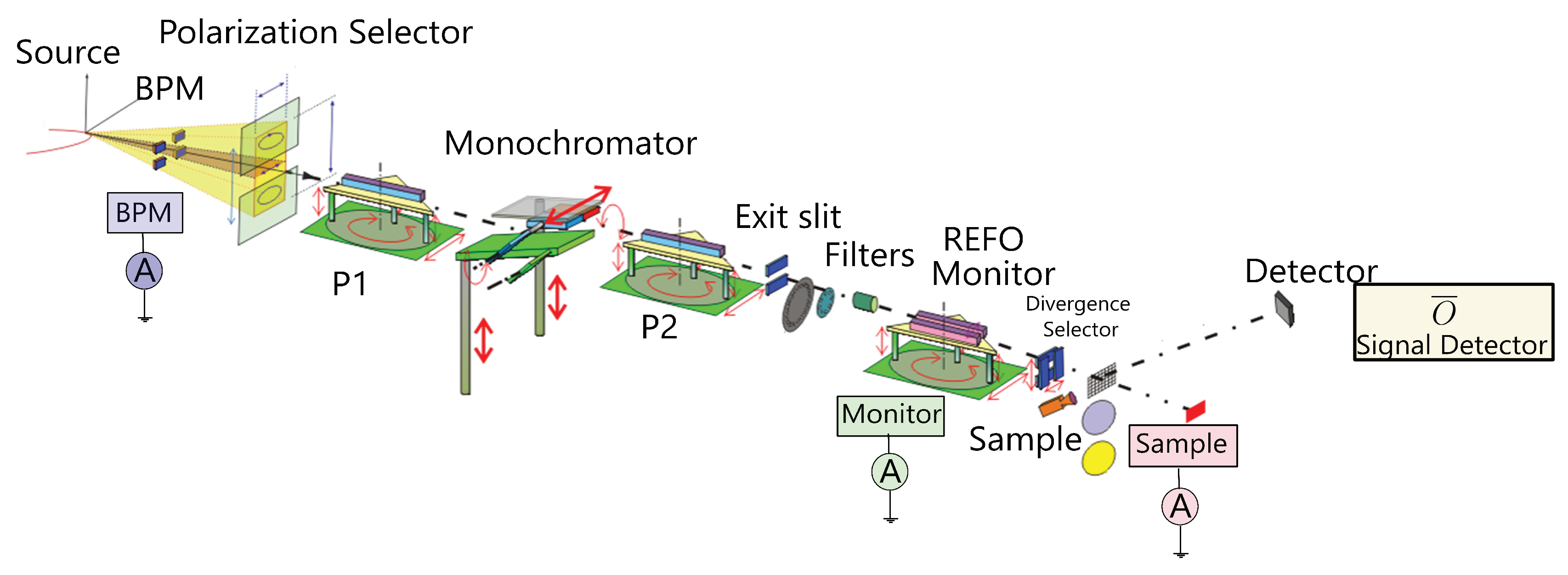
2. Experiment
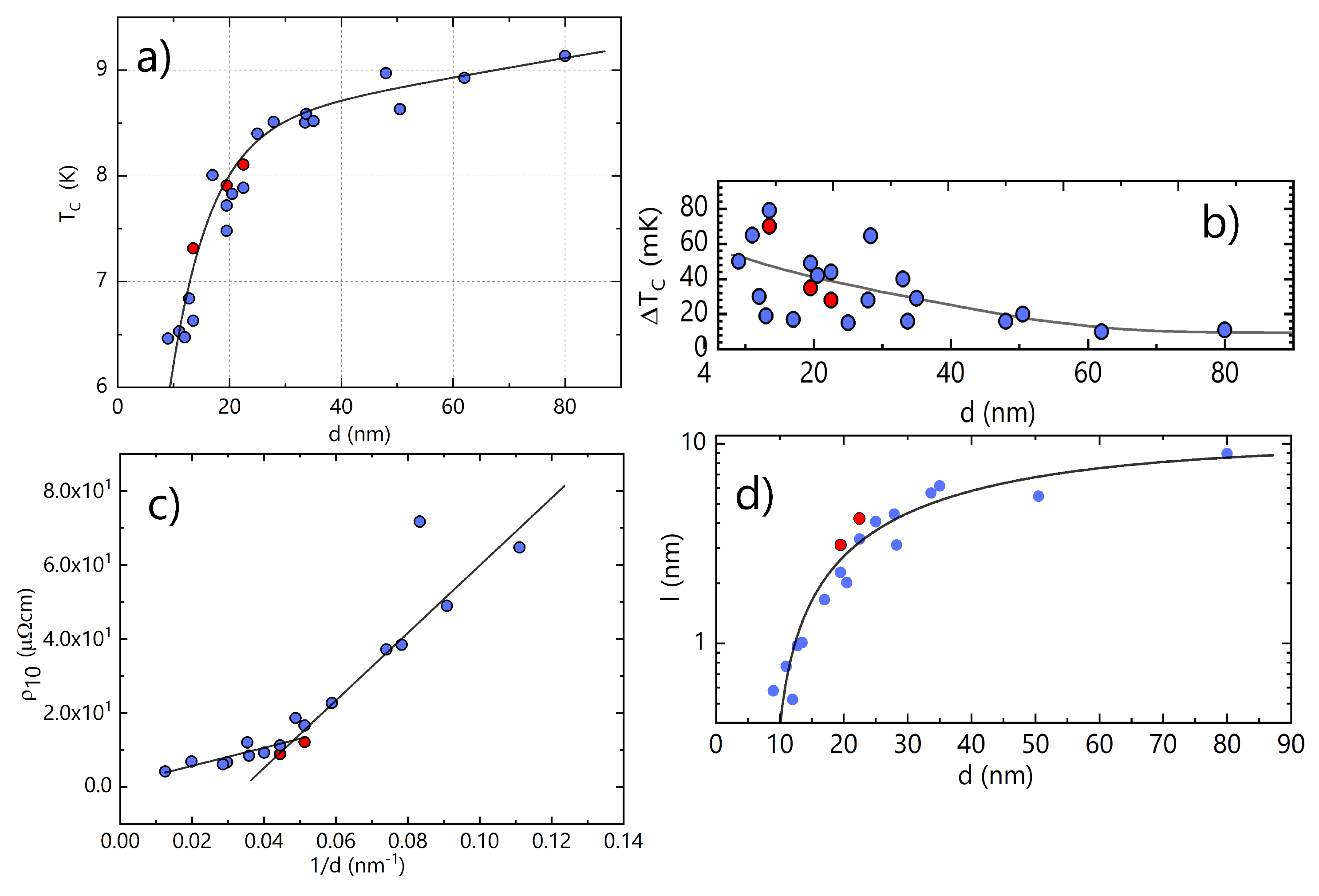
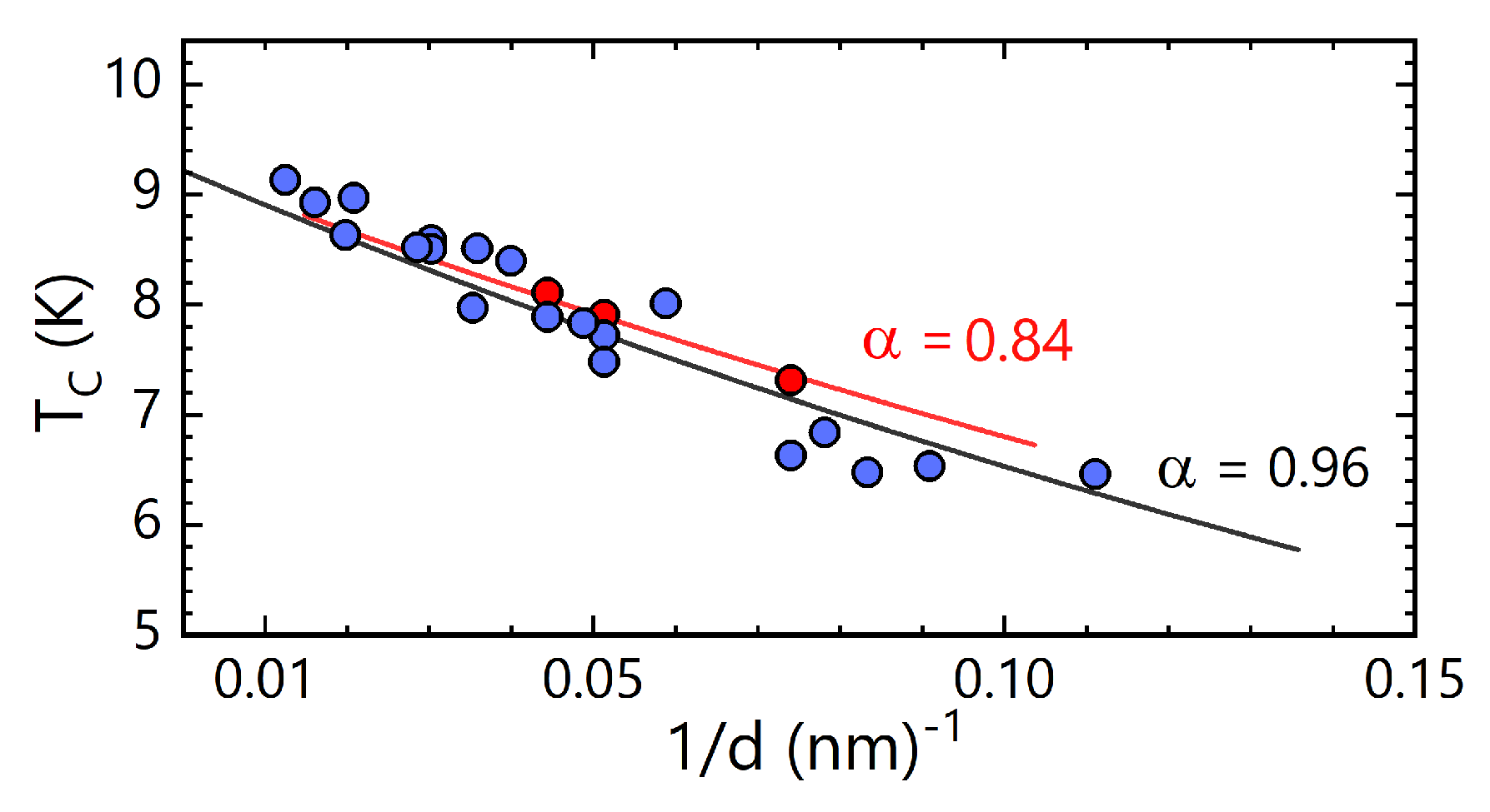
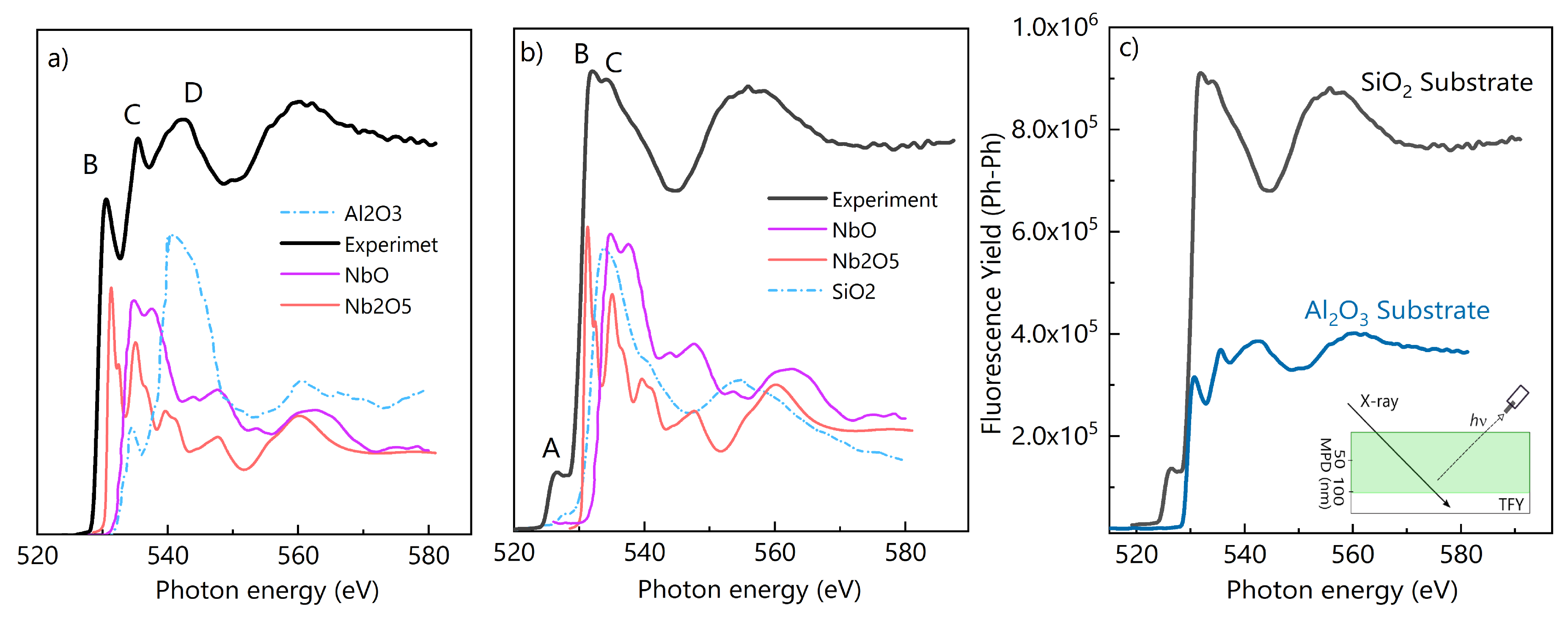
3. Results and Discussion
4. Conclusions
Author Contributions
Funding
Acknowledgments
Conflicts of Interest
References
- Zhang, T.; Cheng, P.; Li, W.J.; Sun, Y.J.; Wang, G.; Zhu, X.G.; He, K.; Wang, L.; Ma, X.; Chen, X.; et al. Superconductivity in one-atomic-layer metal films grown on Si(111). Nat. Phys. 2010, 6, 104. [Google Scholar] [CrossRef]
- Delfanazari, K.; Puddy, R.K.; Ma, P.; Yi, T.; Cao, M.; Gul, Y.; Farrer, I.; Ritchie, D.A.; Joyce, H.J.; Kelly, M.J.; et al. Proximity induced superconductivity in indium gallium arsenide quantum wells. J. Magn. Magn. Mater. 2018, 459, 282–284. [Google Scholar] [CrossRef]
- Sarma, S.D.; Hui, H.Y.; Brydon, P.M.; Sau, J.D. Substrate-induced Majorana renormalization in topological nanowires. New J. Phys. 2015, 17, 075001. [Google Scholar] [CrossRef] [Green Version]
- Delfanazari, K.; Puddy, R.K.; Ma, P.; Yi, T.; Cao, M.; Gul, Y.; Farrer, I.; Ritchie, D.A.; Joyce, H.J.; Kelly, M.J.; et al. On-Chip Andreev Devices: Hard Superconducting Gap and Quantum Transport in Ballistic Nb–In0.75Ga0.25As-Quantum-Well–Nb Josephson Junctions. Adv. Mater. 2017, 29, 1701836. [Google Scholar] [CrossRef] [PubMed]
- Savinov, V.; Delfanazari, K.; Fedotov, V.A.; Zheludev, N.I. Giant nonlinearity in a superconducting sub-terahertz metamaterial. Appl. Phys. Lett. 2016, 108, 101107. [Google Scholar] [CrossRef] [Green Version]
- Semenov, A.; Engel, A.; Il’in, K.; Gol’tsman, G.; Siegel, M.; Hübers, H.W. Ultimate performance of a superconducting quantum detector. Eur. Phys. J. Appl. Phys. 2003, 21, 171–178. [Google Scholar] [CrossRef]
- Karasik, B.S.; Gaidis, M.C.; McGrath, W.R.; Bumble, B.; LeDuc, H.G. Low noise in a diffusion-cooled hot-electron mixer at 2.5 THz. Appl. Phys. Lett. 1997, 71, 1567–1569. [Google Scholar] [CrossRef]
- Mazziotti, M.V.; Valletta, A.; Campi, G.; Innocenti, D.; Perali, A.; Bianconi, A. Possible Fano resonance for high-T c multi-gap superconductivity in p-Terphenyl doped by K at the Lifshitz transition. Europhys. Lett. 2017, 118, 37003. [Google Scholar] [CrossRef] [Green Version]
- Cariglia, M.; Vargas-Paredes, A.; Doria, M.M.; Bianconi, A.; Milošević, M.V.; Perali, A. Shape-Resonant Superconductivity in Nanofilms: from Weak to Strong Coupling. J. Supercond. Novel Magn. 2016, 29, 3081–3086. [Google Scholar] [CrossRef] [Green Version]
- Innocenti, D.; Poccia, N.; Ricci, A.; Valletta, A.; Caprara, S.; Perali, A.; Bianconi, A. Resonant and crossover phenomena in a multiband superconductor: tuning the chemical potential near a band edge. Phys. Rev. B 2010, 82, 184528. [Google Scholar] [CrossRef]
- Guidini, A.; Perali, A. Band-edge BCS-BEC crossover in a two-band superconductor: physical properties and detection parameters. Supercond. Sci. Technol. 2014, 27, 124002. [Google Scholar] [CrossRef]
- Bianconi, A.; Innocenti, D.; Valletta, A.; Perali, A. Shape Resonances in superconducting gaps in a 2DEG at oxide-oxide interface. J. Phys. Conf. Ser. 2014, 529, 012007. [Google Scholar] [CrossRef]
- Milosevic, M.V.; Perali, A. Emergent phenomena in multicomponent superconductivity: An introduction to the focus issue. Supercond. Sci. Technol. 2015, 28, 060201. [Google Scholar] [CrossRef]
- Oya, G.; Koishi, M.; Sawada, Y. High-quality single-crystal Nb films and influences of substrates on the epitaxial growth. J. Appl. Phys. 1986, 60, 1440–1446. [Google Scholar] [CrossRef]
- De Gennes, P.G. Superconductivity of Metals and Alloys; CRC Press: Boca Raton, FL, USA, 2013. [Google Scholar]
- Pinto, N.; Rezvani, S.J.; Favre, L.; Berbezier, I.; Fretto, M.; Boarino, L. Geometrically induced electron-electron interaction in semiconductor nanowires. Appl. Phys. Lett. 2016, 109. [Google Scholar] [CrossRef]
- Rezvani, S.J.; Pinto, N.; Enrico, E.; D’Ortenzi, L.; Chiodoni, A.; Boarino, L. Thermally activated tunneling in porous silicon nanowires with embedded Si quantum dots. J. Phys. D Appl. Phys. 2016, 49, 105104. [Google Scholar] [CrossRef]
- Pinto, N.; Rezvani, S.J.; Perali, A.; Flammia, L.; Milošević, M.V.; Fretto, M.; Cassiago, C.; De Leo, N. Dimensional crossover and incipient quantum size effects in superconducting niobium nanofilms. Sci. Rep. 2018, 8, 4710. [Google Scholar] [CrossRef]
- Chen, Y.J.; Shanenko, A.A.; Perali, A.; Peeters, F.M. Superconducting nanofilms: molecule-like pairing induced by quantum confinement. J. Phys. Cond. Matter 2012, 24, 185701. [Google Scholar] [CrossRef] [Green Version]
- Palestini, F.; Strinati, G.C. Systematic investigation of the effects of disorder at the lowest order throughout the BCS-BEC crossover. Phys. Rev. B 2013, 88, 174504. [Google Scholar] [CrossRef]
- Nannarone, S.; Borgatti, F.; DeLuisa, A.; Doyle, B.P.; Gazzadi, G.C.; Giglia, A.; Finetti, P.; Mahne, N.; Pasquali, L.; Pedio, M.; et al. The BEAR Beamline at Elettra. In AIP Conference Proceedings; AIP Publishing LLC: Melville, NY, USA, 2004; Volume 705, pp. 450–453. [Google Scholar] [CrossRef]
- Pasquali, L.; De Luisa, A.; Nannarone, S. The UHV Experimental Chamber For Optical Measurements (Reflectivity and Absorption) and Angle Resolved Photoemission of the BEAR Beamline at ELETTRA. In AIP Conference Proceedings; AIP Publishing LLC: Melville, NY, USA, 2004; Volume 705, pp. 1142–1145. [Google Scholar] [CrossRef]
- Rezvani, S.J.; Nobili, F.; Gunnella, R.; Ali, M.; Tossici, R.; Passerini, S.; Di Cicco, A. SEI Dynamics in Metal Oxide Conversion Electrodes of Li-Ion Batteries. J. Phys. Chem. C 2017, 121, 26379–26388. [Google Scholar] [CrossRef]
- BEAR Beamline. Available online: https://www.elettra.trieste.it/it/lightsources/elettra/elettra-beamlines/bear/bear.html (accessed on 20 December 2018).
- Lide, D.R. (Ed.) Properties of Solids: Electrical Resistivity of Pure Metals; CRC Press: Boca Raton, FL, USA, 2003. [Google Scholar]
- Dean, J.A. (Ed.) Electronic Configuration and Properties of the Elements; McGraw-Hill: New York, NY, USA, 1999. [Google Scholar]
- Hazra, D.; Datta, S.; Mondal, M.; Ghatak, J.; Satyam, P.V.; Gupta, A.K. Thickness dependent lattice expansion in nanogranular Nb thin films. J. Appl. Phys. 2008, 103, 103535. [Google Scholar] [CrossRef]
- Hazra, D.; Mondal, M.; Gupta, A.K. Correlation between structural and superconducting properties of nano-granular disordered Nb thin films. Phys. C Supercond. Appl. 2009, 469, 268–272. [Google Scholar] [CrossRef]
- Zhao, L.; Jin, Y.; Li, J.; Deng, H.; Li, H.; Huang, K.; Cui, L.; Zheng, D. Fabrication of Nb Superconducting Nanowires by Nanoimprint Lithography. IEEE Trans. Appl. Supercond. 2015, 25, 2200605. [Google Scholar] [CrossRef]
- Delacour, C.; Ortega, L.; Faucher, M.; Fournier, T.; Pannetier, B.; Bouchiat, V. Persistence of superconductivity in niobium ultrathin films grown on R-plane sapphire. Phys. Rev. B 2011, 83, 144504–144508. [Google Scholar] [CrossRef]
- Gubin, A.; Il’in, K.; Vitusevich, S.; Siegel, M.; Klein, N. Dependence of magnetic penetration depth on the thickness of superconducting Nb thin films. Phys. Rev. B 2005, 72, 064503–064508. [Google Scholar] [CrossRef]
- Bose, S.; Raychaudhuri, P.; Banerjee, R.; Vasa, P.; Ayyub, P. Mechanism of the size dependence of the superconducting transition of nanostructured Nb. Phys. Rev. Lett. 2005, 95, 147003. [Google Scholar] [CrossRef] [PubMed]
- Gershenzon, M.; Koshelets, V. Study of superconducting properties of Nb and NbN films obtained by method of high particle cathode atomization. Zh. Tekh. Fiz. 1980, 50, 572. [Google Scholar]
- Bianconi, A.; MArcelli, A. Synchrotron Radiation Research: Advances in Surface And Interface Science Techniques; Springer: Boston, MA, USA, 1992; pp. 63–115. [Google Scholar]
- Rezvani, S.; Pinto, N.; Perali, A.; Nannarone, S. Interfacial Nb oxidation on silicon oxide and sapphire studied by x-ray absorption and reflection spectroscopy. In preparation.
- McMillan, W.L. Tunneling Model of the Superconducting Proximity Effect. Phys. Rev. 1968, 175, 537–542. [Google Scholar] [CrossRef]
- Shanenko, A.A.; Croitoru, M.D.; Peeters, F.M. Quantum-size effects on TC in superconducting nanofilms. Europhys. Lett. 2006, 76, 498–504. [Google Scholar] [CrossRef]


| Substrate | Thickness (nm) | (K) | (mK) | (cm) | l (nm) |
|---|---|---|---|---|---|
| SiO2 | 9.0 | 6.46 | 50 | 64.70 | 0.58 |
| SiO2 | 11.0 | 6.53 | 65 | 48.90 | 0.77 |
| SiO2 | 12.0 | 6.47 | 30 | 71.70 | 0.52 |
| SiO2 | 13 | 6.84 | 19 | 38.44 | 0.98 |
| SiO2 | 19.5 | 7.48 | 49 | 16.56 | 2.26 |
| SiO2 | 22.5 | 7.89 | 44 | 11.25 | 3.33 |
| SiO2 | 25 | 8.40 | 15 | 9.23 | 4.06 |
| SiO2 | 28.0 | 8.51 | 28 | 8.45 | 4.44 |
| SiO2 | 28.0 | 7.97 | 65 | 12.05 | 3.11 |
| SiO2 | 34.0 | 8.58 | 16 | 6.63 | 5.66 |
| SiO2 | 35.0 | 8.519 | 29 | 6.11 | 6.14 |
| SiO2 | 50.0 | 8.63 | 20 | 6.87 | 5.46 |
| SiO2 | 80.0 | 9.13 | 11 | 4.21 | 8.91 |
| Al2O3 | 13.5 | 7.313 | 75 | - | - |
| Al2O3 | 19.5 | 7.91 | 35 | 12.08 | 3.10 |
| Al2O3 | 22.5 | 8.11 | 28 | 8.90 | 4.21 |
© 2018 by the authors. Licensee MDPI, Basel, Switzerland. This article is an open access article distributed under the terms and conditions of the Creative Commons Attribution (CC BY) license (http://creativecommons.org/licenses/by/4.0/).
Share and Cite
Rezvani, S.J.; Perali, A.; Fretto, M.; De Leo, N.; Flammia, L.; Milošević, M.; Nannarone, S.; Pinto, N. Substrate-Induced Proximity Effect in Superconducting Niobium Nanofilms. Condens. Matter 2019, 4, 4. https://doi.org/10.3390/condmat4010004
Rezvani SJ, Perali A, Fretto M, De Leo N, Flammia L, Milošević M, Nannarone S, Pinto N. Substrate-Induced Proximity Effect in Superconducting Niobium Nanofilms. Condensed Matter. 2019; 4(1):4. https://doi.org/10.3390/condmat4010004
Chicago/Turabian StyleRezvani, S.J., Andrea Perali, Matteo Fretto, Natascia De Leo, Luca Flammia, Milorad Milošević, Stefano Nannarone, and Nicola Pinto. 2019. "Substrate-Induced Proximity Effect in Superconducting Niobium Nanofilms" Condensed Matter 4, no. 1: 4. https://doi.org/10.3390/condmat4010004
APA StyleRezvani, S. J., Perali, A., Fretto, M., De Leo, N., Flammia, L., Milošević, M., Nannarone, S., & Pinto, N. (2019). Substrate-Induced Proximity Effect in Superconducting Niobium Nanofilms. Condensed Matter, 4(1), 4. https://doi.org/10.3390/condmat4010004