Article

Energy Response of Silicon Drift Detectors for Kaonic Atom Precision Measurements

1
Istituto Nazionale di Fisica Nucleare–Laboratori Nazionali di Frascati (LNF-INFN), 00044 Frascati RM, Italy
2
Department of Physics, Faculty of Science MM.FF.NN., University of Rome 2 (Tor Vergata), 00133 Rome, Italy
3
Politecnico di Milano, Dipartimento di Elettronica, Informazione e Bioingegneria and INFN Sezione di Milano, 20133 Milano, Italy
4
Horia Hulubei National Institute of Physics and Nuclear Engineering (IFIN-HH), 77125 Magurele, Romania
5
Stefan-Meyer-Institut für Subatomare Physik, 1090 Vienna, Austria
*
Author to whom correspondence should be addressed.
Condens. Matter 2019, 4(1), 31; https://doi.org/10.3390/condmat4010031
Submission received: 29 January 2019 / Revised: 1 March 2019 / Accepted: 6 March 2019 / Published: 11 March 2019
(This article belongs to the Special Issue High Precision X-Ray Measurements)

Abstract

:
Novel, large-area silicon drift detectors (SDDs) have been developed to perform precision measurements of kaonic atom X-ray spectroscopy, for the study the K ¯ N strong interaction in the low-energy regime. These devices have special geometries, field configurations and read-out electronics, resulting in excellent performances in terms of linearity, stability and energy resolution. In this work the SDDs energy response in the energy region between 4000 eV and 12,000 eV is reported, revealing a stable linear response within 1 eV and good energy resolution.

1. Introduction

The main advantage of semiconductor X-ray detectors is the much lower energy required to create electron-hole pairs with respect to a gas detector, giving a greater number of charge carriers produced and, consequently, a better energy resolution. A silicon drift detector (SDD) consists of a double sided fully depleted silicon wafer with a cylindrical shape [1,2,3] where the n bulk is sided by a p + concentric ring strips and p + non-structured layer which forms the radiation entrance window. The radial drift field focuses the electrons produced by the absorbed radiation to the n + small anode placed in the centre of the p + strips side. The small value of the anode capacitance increases the amplitude of the output signal, giving good energy resolution and low noise in the subsequent electronic components also in high-count rate measurements. Since the anode capacitance is independent from the active area [4], these detectors can be built with a large active area. Furthermore, thanks to their reduced thickness, they can handle background events caused by high-energy particles still maintaining almost 100% efficiency for 8 keV X-rays.
The development of new SDD technologies dedicated to kaonic atom spectroscopy brought improvement in device performance with respect to past silicon detectors, allowing more precise and challenging measurements [5,6,7,8,9,10,11]. New monolithic SDD arrays have been developed by Fondazione Bruno Kessler (FBK, Italy), together with Politecnico di Milano (PoliMi, Italy), Istituto Nazionale di Fisica Nucleare-Laboratori Nazionali di Frascati (LNF-INFN, Italy) and Stefan Meyer Institute (SMI, Austria), to perform precise measurements of kaonic atom transitions at LNF-INFN and J-PARC.
The characterization and optimization of the energy response of the SDD detectors under temperature and voltage variations will be reported.

2. Materials and Methods

The SDD monolithic array is 450 μ m thick and consists of a 2 × 4 matrix of square cells, each with an active area of 0.64 mm 2 , glued on an Alumina carrier. The ceramic carrier provides a common polarization for all the devices to the following electrodes: The ring closest to the anode (R1), the outermost ring (RN) on the p + rings side and to the non-structured contact on the opposite side (Back). Keeping the voltage supplied to the R1 fixed at 15 V and moving the biasing of RN and Back (with fixed ratio RN/Back = 2), one can adjust the drift field inside the detector (V D r i f t ), optimizing the electron collection to the anode.
The ceramic carrier is screwed on top of an aluminium holder block, to protect the bonding and to cool the SDDs down to 120 K. The detector is placed inside a vacuum chamber (Figure 1a) with a Φ = 60 mm mylar window on top, a CONFLAT DN40 flange on one side for vacuum pumping and two Fischer (20 pin) vacuum connectors both for detector feed-throughs and temperature-pressure readings. The high vacuum (10 7 mbar) inside the chamber is obtained by a 80 L/s dry turbo molecular pump and a dry multistage “scroll” pump, which avoids detector surface contamination during the cooling. A dry air (high purity N 2 gas) flux keeps the system clean when the pumping is off and speeds up the detector heating from 250 K to room temperature without adding contaminants.
The detector is screwed on a cold finger attached to an external cryostat, providing any intermediate temperature between 100 K and 250 K with a stability of 0.1 K. An additional detector surface protection, made by a suitable aluminium support, surrounds the detector and holds a 7.25 μ m Mylar foil to prevent any residual gas condensation on its surface during the cooling.
Lastly, Al-Mylar foils shield the internal walls close to the cold finger from radiative heating.
The target is made of strips of titanium (Ti), iron (Fe) and copper (Cu) fixed on an epoxy plate encapsulating powder of potassium bromine (KBr) and provides fluorescent emission lines in the range 4500 eV to 12000 eV. The target is anchored on an aluminium support at 45° with respect to the detector surface, as showed in Figure 1b. A tungsten (W) anode X-ray tube (HXR 55-50-01, Oxford Instruments, Abingdon, UK) shines on the target parallel to the entrance window, inducing the X-ray fluorescence. This “reflection-like” configuration optimizes the solid angle for both the detector placement and the X-ray activation beam, maximizing the signal over background ratio.

3. Results and Discussion

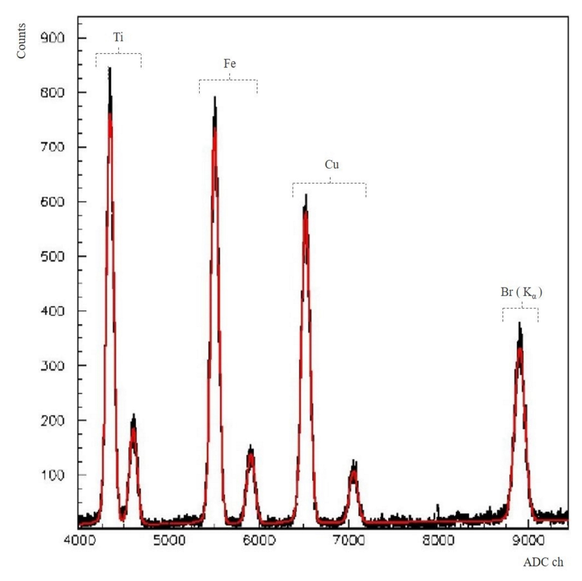
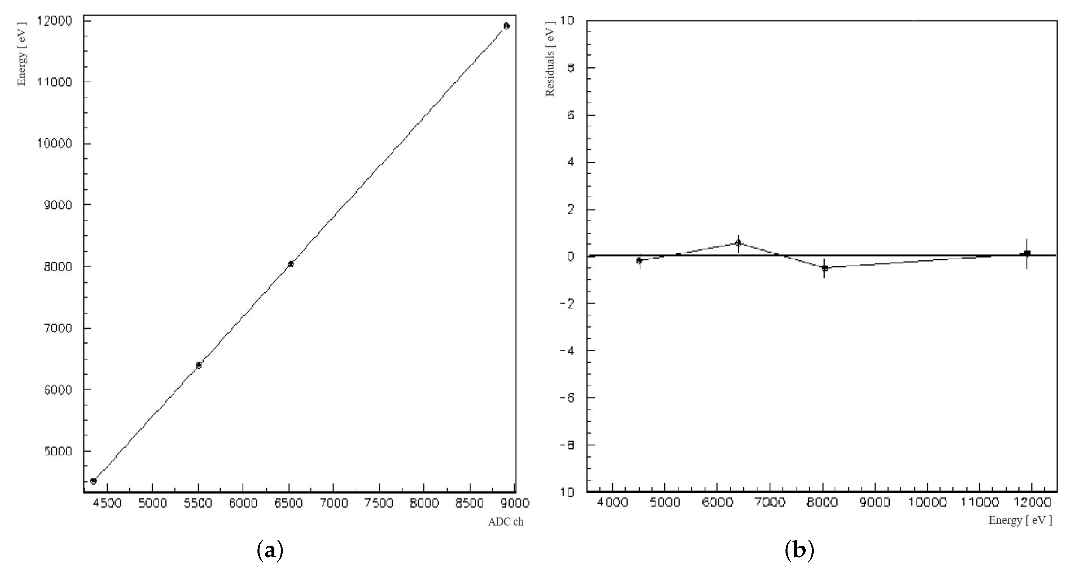
3.1. Energy Calibration
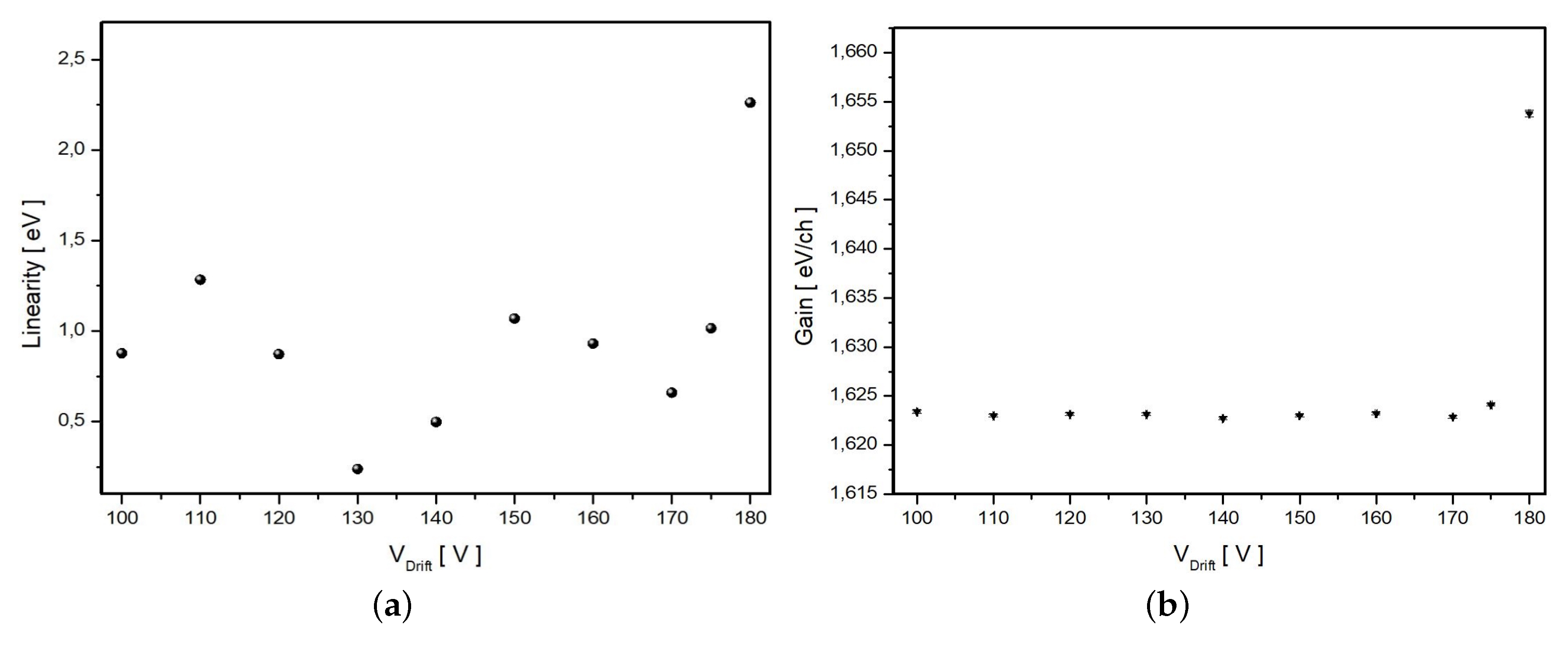
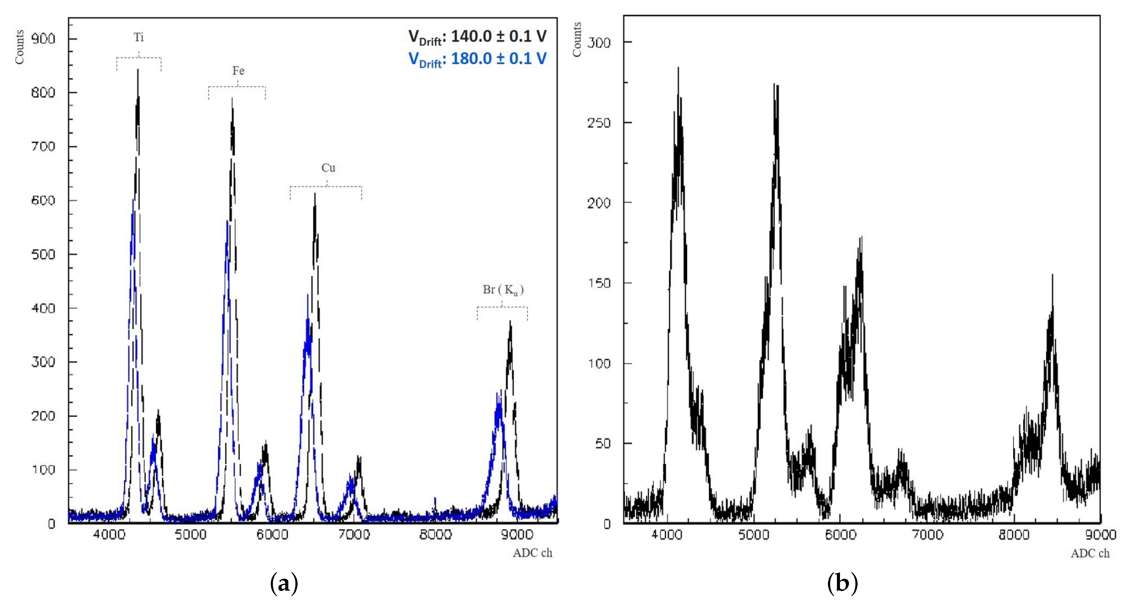
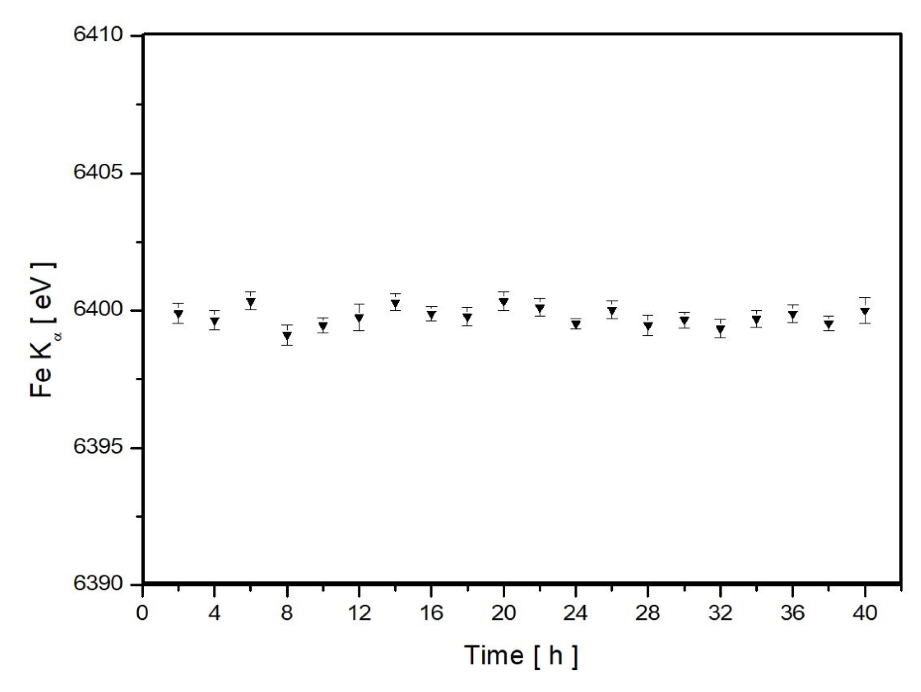
The collected spectra have been calibrated in energy using the K α peaks of the excited elements of the target, fitted with a single function consisting in a sum of Gaussians and tails for the fluorescence lines and an exponential function to describe the background [12]. As an example, Figure 2 shows the fitted spectrum used for the calibration of a fluorescence spectrum obtained at T S D D = 121.6 ± 0.1 K and V D r i f t = 140.0 ± 0.1 V. A linear fit interpolates the calibration points, whose coordinates are the theoretical (P i l a b e l ) and the experimental values of each K α peak, as showed in Figure 3a. The slope of the function, in eV/ch units, gives the gain parameter (g) of the spectrum. The difference between each K α calibrated position (P i c a l ), with respect to its corresponding theoretical value, gives the residual plot shown in the Figure 3b, used for the evaluation of the system linearity. The distribution reveals that the distance of each calibrated peak from the theoretical value is below 1 eV, so the systematic error in the evaluation of the peak position over the whole energy region is better than 1 eV.
The procedure has been performed for a set of measurements, collected by varying V D r i f t , evaluating the linearity parameter (l) by using Equation (1):
l = 1 4 ( P i l a b e l P i c a l ) 2 4
Keeping fixed the R1 polarization at 15.0 ± 0.1 V and the SDD temperature at 121.6 ± 0.1 K, a linearity and gain study has been performed in the V D r i f t range between 100–180 V, with the results summarized in Figure 4. Starting from the lower voltage up to 175.0 ± 0.1 V the distribution of the points is stable for both residuals and gain. For the points below 175 V, the mean value of the linearity is set around 1 eV, consistent with the previous evaluation. By moving the V D r i f t up to 180 V, the excellent linear response of the system is suddenly lost, resulting in an increment of the residuals up to 2.5 eV.
This trend is reflected also in the gain plot, which presents a sharp rise at V D r i f t = 180.0 ± 0.1 V. It reveals that the peak position on the ADC spectra are shifted downward with respect to the lower voltages, as shown also in Figure 5a, where the overlap of two non-calibrated spectra collected at different V D r i f t are presented. This behaviour indicates a reduced amount of charge collected to the anode. The incomplete charge collection is related to the high voltage applied, which moves the focus of the drift field away from the anode [13]. In addition to the previous considerations, Figure 5b shows that the spectrum collected 2 V above 180 V, presents also a sensible energy resolution worsening.

3.2. Stability

An important aspect of the SDD system to be used in kaonic atom experiments is its stability over a long running period. To evaluate it, a spectrum collected over two days of running has been sampled in intervals of two hours.
The following parameters of the data taking were stable during the test:
  • X-ray tube voltage: 23.0 ± 0.1 kV;
  • X-ray tube current: 10.0 ± 0.1 μ A;
  • SDDs temperature: 121.6 ± 0.1 K;
  • SDDs V D r i f t : 140.0 ± 0.1 V;
The stability has been verified from the calibrated values of the Fe K α peak, using the K α lines of titanium and bromine to obtain the ADC to eV conversion of the spectrum.
The results are plotted in Figure 6.
The values obtained from the analysis are fluctuating around the reference value of the Fe K α line (the weighted mean value of Fe K α 1 and K α 2 is 6399.64 eV). An oscillating trend, with an amplitude around 1 eV is present. This can be due to temperature variations between day and night in the laboratory, which affect the readout electronic. The mean value of the calibrated peak position over the whole range is 6399.8 ± 0.4 eV and differs by 0.2 eV from the reference value, consistently with the systematic error previously evaluated.

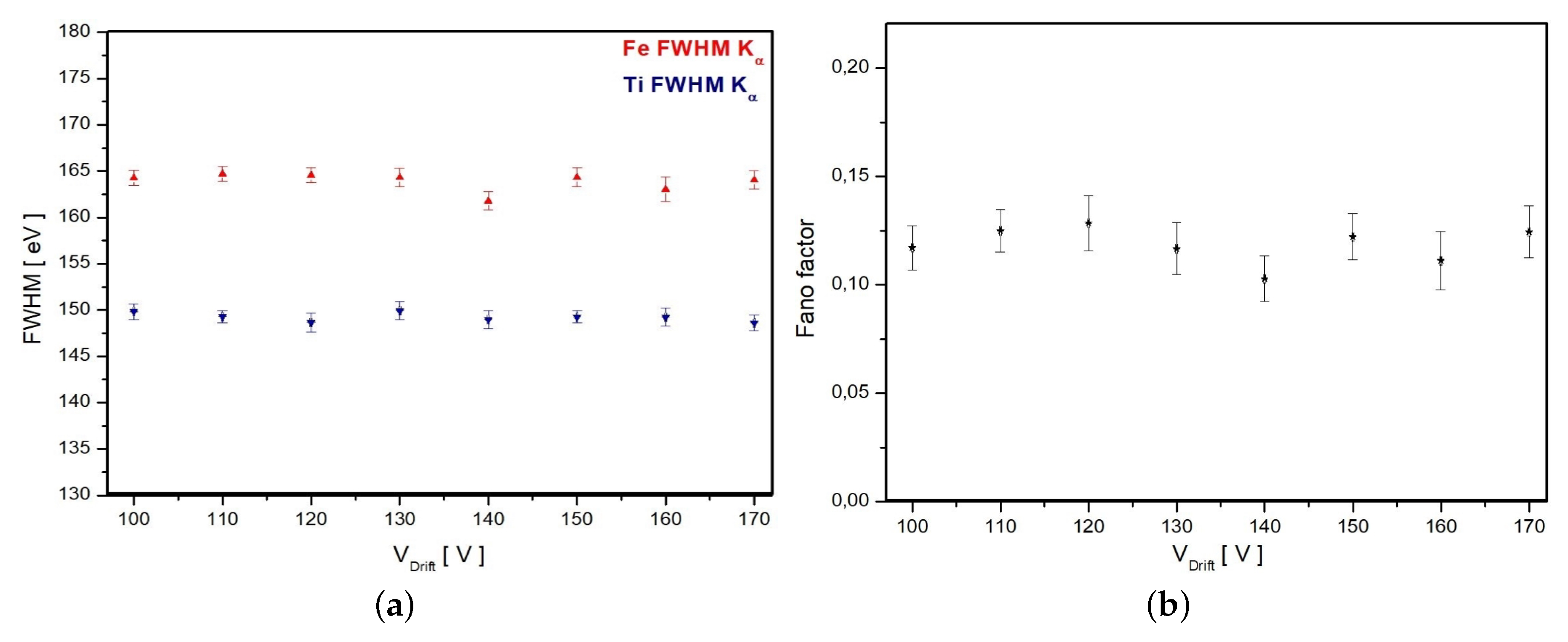
3.3. Energy Resolution

The energy resolution reflects the detector accuracy in the determination of the incoming radiation energy. For the SDDs, the total energy resolution ( Δ E t o t 2 ) results from the sum of three distinct contributions, as described by Equation (2):
Δ E t o t 2 = Δ E i n t r 2 + Δ E e . n . 2 + Δ E c . c . 2
where:
  • Δ E i n t r 2 is the intrinsic spread given by the statistical fluctuation in the number of the charge created by the incoming radiation. For a Gaussian distribution, it is due to the energy of the line ( E i ), the electron hole pair creation energy ( ϵ ) and the correction of the Fano factor (F), accordingly to the relation Δ E i n t r 2 = ( 2.35 ) 2 · F · ϵ · E i ;
  • Δ E e . n . 2 is the thermal and electronic noise contribution;
  • Δ E c . c . 2 is due to the incomplete charge collection;
As showed in the previous analysis concerning the linear response of the detectors, the contribution due to the incomplete charge collection is negligible below 180 V.
The energy resolution has been investigated as a function both of drift field and temperature, and, given ϵ [14], the Fano factor has been extracted from the Fe K α and Ti K α peaks.
Figure 7a shows the FWHM, expressed in eV, of Fe K α and Ti K α in the range between 100.0 V and 170.0 V, for a fixed temperature of 123.1 ± 0.1 K. The red dots are for Fe K α FWHM, while the blue dots are for Ti K α FWHM. The width of the peaks is stable over the scan, meaning that the energy resolution of the SDD is not sensitive to the bias of the electrodes inside a wide range of applied V D r i f t . The intrinsic contribution of the detector resolution, resulting from the obtained values of the Fano factor, reflects that the Gaussian widening of the peak, due to the pair creation statistics, is not affected by the drift field in the investigated range. The mean value experimentally obtained for the Fano factor is 0.118 ± 0.009.
A temperature scan has been done fixing V D r i f t at 140.0 ± 0.1 V and increasing the detector temperature from 123.1 ± 0.1 K up to 233.1 ± 0.1 K. Figure 8a shows that the energy resolution is quite constant below 170 K, while a relevant peak broadening is detected starting from 180 K up. For this study, the Fano factor results to be stable (Figure 8b), with a mean value of 0.116 ± 0.009, compatible to the previous result. Since the intrinsic contribution of the peak widening is not affected by the temperature as demonstrated by the Fano factor distribution, the energy resolution worsening with the temperature is associated to an higher thermal noise inside the detector. Its increment is due to the larger number of carriers created by thermal excitation (leakage current). Thus, a progressive cooling of the device ensures lower leakage current, as well as higher performances in terms of energy resolution.

4. Conclusions

The work presented in this paper qualifies and optimizes the new technology of silicon drift detectors to be used for precision measurements of kaonic atom X-ray transitions. The detectors are stable and linear within 1 eV in the energy range between 4500–12000 eV, which means that the relative systematic error is at the level of 10 4 . The voltage scan grants that the common polarization of the eight units of the matrix has no drawbacks in terms of linearity for a wide range, below an upper limit set by a not efficient charge collection to anode. Likewise, the energy resolution is not affected by the variation of the drift field inside the detector, in the range of the stable linear response. The intrinsic resolution, extracted by the width of the Ti and Fe K α peaks, results as independent from the collecting field, giving a mean value for the Fano factor equal to 0.118 ± 0.009.
A temperature scan shows that the widening of the peaks is due to an increment of the leakage current inside the detector, testifying that the cooling of the device ensures the best performances. The intrinsic contribution is constant, resulting in a Fano factor value of 0.116 ± 0.009.
The analysis of the silicon drift detector energy response presented in this work optimizes the working conditions of the device, indicating them as excellent candidates for precision measurements of kaonic atom X-ray transitions.

Author Contributions

Conceptualization, M.M. and M.I.; software, M.I.; validation, M.M., M.I. and C.C.; formal analysis, M.M. and A.S.; investigation, M.M.; resources, M.M., A.A., M.B., F.S., C.F. and J.Z.; data curation, M.M.; writing—original draft preparation, M.M.; writing—review and editing, M.M.; administration, M.M., M.I. and C.C.; funding acquisition, C.C., C.F. and J.Z.

Funding

Part of this work was supported by the Austrian Science Fund (FWF): [P24756-N20]; Austrian Federal Ministry of Science and Research BMBWK 650962/0001 VI/2/2009; the Croatian Science Foundation, project IP2018-01-8570; Ministero degli Affari Esteri e della Cooperazione Internazionale, Direzione Generale per la Promozione del Sistema Paese (MAECI), StrangeMatter project; Polish National Science Center through grant no. UMO-2016/21/D/ ST2/01155; Ministry of Science and Higher Education of Poland grant no 7150/E338/M/2018.

Conflicts of Interest

The authors declare no conflict of interest.

References

  1. Gatti, E.; Rehak, P. Semiconductor drift chamber—An application of a novel charge transport scheme. Nucl. Instrum. Meth. Phys. Res. 1984, 225, 608–614. [Google Scholar] [CrossRef]
  2. Gatti, E.; Rehak, P. Silicon drift chambers—First results and optimum processing of signals. Nucl. Instrum. Meth. Phys. Res. A 1984, 226, 129–141. [Google Scholar] [CrossRef]
  3. Lechner, P.; Eckbauer, S.; Hartmann, R.; Krisch, S.; Hauff, D.; Richter, R.; Soltau, H.; Strüder, L.; Fiorini, C.; Gatti, E.; et al. Silicon drift detectors for high resolution room temperature X-ray spectroscopy. Nucl. Instrum. Meth. Phys. Res. A 1996, 377, 346–351. [Google Scholar] [CrossRef]
  4. Rehak, P.; Gatti, E.; Longoni, A.; Kemmer, J.; Holl, P.; Klanner, R.; Lutz, G.; Wylie, A. Semiconductor drift chambers for position and energy measurements. Nucl. Instrum. Meth. Phys. Res. A 1985, 235, 224–234. [Google Scholar] [CrossRef]
  5. Iwasaki, M.; Hayano, R.S.; Ito, T.M.; Nakamura, S.N.; Terada, T.P.; Gill, D.R.; Lee, L.; Olin, A.; Salomon, M.; Yen, S.; et al. Observation of Kaonic Hydrogen Kα X-Rays. Phys. Rev. Lett. 1997, 78, 3067–3069. [Google Scholar] [CrossRef]
  6. Bazzi, M.; Beer, G.; Bombelli, L.; Bragadireanu, A.M.; Cargnelli, M.; Corradi, G.; Curceanu, C.P.; d’Uffizi, A.; Fiorini, C.; Frizzi, T.; et al. A new measurement of kaonic hydrogen X-rays. Phys. Lett. B 2011, 704, 113–117. [Google Scholar] [CrossRef] [Green Version]
  7. Okada, S.; Beer, G.; Bhang, H.; Cargnelli, M.; Chiba, J.; Choi, S.; Curceanu, C.; Fukuda, Y.; Hanaki, T.; Hayano, R.S.; et al. Precision measurement of the 3d→2p X-ray energy in kaonic 4He. Phys. Lett. B 2007, 653, 387–391. [Google Scholar] [CrossRef]
  8. Bazzi, M.; Beer, G.; Bombelli, L.; Bragadireanu, A.M.; Cargnelli, M.; Corradi, G.; Curceanu, C.; d’Uffizi, A.; Fiorini, C.; Frizzi, T.; et al. Kaonic helium-4 X-ray measurement in SIDDHARTA. Phys. Lett. B 2009, 681, 310–314. [Google Scholar] [CrossRef]
  9. Bazzi, M.; Beer, G.; Bombelli, L.; Bragadireanu, A.M.; Cargnelli, M.; Corradi, G.; Curceanu, C.; d’Uffizi, A.; Fiorini, C.; Frizzi, T.; et al. First measurement of kaonic helium-3 X-rays. Phys. Lett. B 2011, 697, 199–202. [Google Scholar] [CrossRef] [PubMed] [Green Version]
  10. Bazzi, M.; Beer, G.; Bellotti, G.; Berucci, C.; Bragadireanu, A.M.; Bosnar, D.; Cargnelli, M.; Curceanu, C.; Butt, A.D.; d’Uffizi, A.; et al. K-series X-ray yield measurement of kaonic hydrogen atoms in a gaseous target. Nucl. Phys. A 2016, 954, 7–16. [Google Scholar] [CrossRef]
  11. Bazzi, M.; Beer, G.; Berucci, C.; Bragadireanu, A.M.; Cargnelli, M.; Curceanu, C.; d’Uffizi, A.; Fiorini, C.; Ghio, F.; Guaraldo, C.; et al. L-series X-ray yields of kaonic 3He and 4He atoms in gaseous targets. Eur. Phys. J. A 2014, 50, 1–4. [Google Scholar] [CrossRef]
  12. Van Gysel, M.; Lemberge, P.; Van Espen, P. Implementation of a spectrum fitting procedure using a robust peak model. X-ray Spectrom. 2003, 32, 434–441. [Google Scholar] [CrossRef]
  13. Bertuccio, C.; Castoldi, A.; Longoni, A.; Sampietro, M.; Gauthier, C. New electrode geometry and potential distribution for soft X-ray drift detectors. Nucl. Instrum. Meth. Phys. Res. A 1992, 312, 613–616. [Google Scholar] [CrossRef]
  14. Mazziotta, M.N. Electron–hole pair creation energy and Fano factor temperature dependence in silicon. Nucl. Instrum. Meth. Phys. Res. A 2008, 584, 436–439. [Google Scholar] [CrossRef]
Figure 1. (a) Top view of SDDs array vacuum chamber; (b) Experimental setup in “reflection like” configuration.
Condensedmatter 04 00031 g001
Figure 2. Fit of the fluorescence spectrum collected with T S D D = 121.6 ± 0.1 K and V D r i f t = 140.0 ± 0.1 V.
Condensedmatter 04 00031 g002
Figure 3. (a) Linear calibration of the spectrum using K α peaks of the four elements; (b) Residuals plot.
Condensedmatter 04 00031 g003
Figure 4. (a) Linearity parameter (l); (b) Gain of the system under voltage scan.
Condensedmatter 04 00031 g004
Figure 5. (a) The overlap of spectrum collected at V D r i f t = 140.0 ± 0.1 V (black) and V D r i f t = 180.0 ± 0.1 V (blue) shows a shift downward of the spectrum; (b) The energy resolution worsening for the spectrum collected at V D r i f t = 182.0 ± 0.1 V reveals that the electron collection is not focused to the anode.
Condensedmatter 04 00031 g005
Figure 6. Calibrated position of Fe K α peak during the stability test run.
Condensedmatter 04 00031 g006
Figure 7. Energy response of the detector under the voltage scan. (a) Distribution of energy resolution of Ti K α (blue) and Fe K α (red) for different drift voltages; (b) Fano factor values at different drift voltages.
Condensedmatter 04 00031 g007
Figure 8. Energy response of the detector under the temperature scan. (a) The widening of Ti K α (blue) and Fe K α (red) peaks are related to the increasing of the detector temperature; (b) Plot of the detector Fano factor at different temperatures reveals that the intrinsic contribution is not affected by the temperature within the experimental error.
Condensedmatter 04 00031 g008

