Abstract
Parallel hardware designed for image processing promotes vision-guided intelligent applications. With the advantages of high-throughput and low-latency, streaming architecture on FPGA is especially attractive to real-time image processing. Notably, many real-world applications, such as region of interest (ROI) detection, demand the ability to process images continuously at different sizes and resolutions in hardware without interruptions. FPGA is especially suitable for implementation of such flexible streaming architecture, but most existing solutions require run-time reconfiguration, and hence cannot achieve seamless image size-switching. In this paper, we propose a dynamically-programmable buffer architecture (D-SWIM) based on the Stream-Windowing Interleaved Memory (SWIM) architecture to realize image processing on FPGA for image streams at arbitrary sizes defined at run time. D-SWIM redefines the way that on-chip memory is organized and controlled, and the hardware adapts to arbitrary image size with sub-100 ns delay that ensures minimum interruptions to the image processing at a high frame rate. Compared to the prior SWIM buffer for high-throughput scenarios, D-SWIM achieved dynamic programmability with only a slight overhead on logic resource usage, but saved up to of the BRAM resource. The D-SWIM buffer achieves a max operating frequency of MHz and reduction in power consumption by comparing with the SWIM scheme. Real-world image processing applications, such as 2D-Convolution and the Harris Corner Detector, have also been used to evaluate D-SWIM’s performance, where a pixel throughput of Giga Pixel/s and Giga Pixel/s were achieved respectively in each case. Compared to the implementation with prior streaming frameworks, the D-SWIM-based design not only realizes seamless image size-switching, but also improves hardware efficiency up to .
1. Introduction
Real-time image processing applications, such as for high-speed image-guided vehicle control [1], requires the underlying image-processing hardware to be both high-throughput and low-latency. Furthermore, for many real-world scenarios, such as in detecting and processing the region of interest (ROI) of arbitrary sizes, the underlying hardware must also be flexible to adapt to the varying input-sized images as needed [2]. With ample high-bandwidth I/O and on-chip programmable logic resources, researchers have demonstrated the benefits of using Field Programmable Gate Arrays (FPGAs) to address the throughput and latency challenges in a wide range of image processing applications. For instance, Wang et al. [3] demonstrated that by using an FPGA to directly process output from a high-speed time-stretch imaging camera, they can successfully classify cell images in real-time with data throughput exceeding 4 Giga Pixels Per Second (GPPS). Similarly, Ma et al. [4] demonstrated an automatic tool for porting general Deep Neural Networks (DNN) to FPGA, which achieves a maximum processing throughput of 710 Giga Operations Per Second (GOPS) and a latency of ms for each image frame.
As illustrated by the above examples, one key to achieving high-throughput low-latency image processing on FPGAs is by leveraging carefully pipelined hardware that can operate on the input image as pixel streams without excessive buffering. These hardware architectures are able to commence processing of the image as soon as the necessary pixels are received and continue processing the rest of the arriving image as a pipeline, giving rise to both low-latency and high-throughput operations. Indeed, to facilitate the design of complex streaming image-processing hardware, some FPGA-hardware generators have already been proposed, often relying on the use of domain-specific languages (DSLs) as a bridge between the algorithm designer and the lower-level hardware [5,6,7,8]. In our previous work, SWIM [9], a streaming line buffer generator, was also proposed to address the complexities of rearranging misaligned multi-pixel blocks for ultra high-input throughput applications. It demonstrated that by carefully arranging on-chip memory resources to align with the input image size, a fully pipelined image processing system on FPGA could be realized that operates close to the FPGA maximum clock frequency.
However, while these hardware generation frameworks can efficiently produce designs for a particular target application, they must be pre-configured to a fixed input image size before the FPGA synthesis. The FPGA has to be reconfigured when the input image size changes, limiting their use in real-time applications that operate on input images with varying sizes.
Building on top of the work of SWIM, we present in this paper an improved high-throughput hardware architecture that can adapt to the size of the input image dynamically during runtime without hardware reconfiguration. The improved scheme, called Dynamic-SWIM (D-SWIM), utilizes an improved on-chip memory organization that can adapt to changing the image size dynamically. Different to SWIM, the D-SWIM framework generates light-weighted control instructions for different image sizes. The hardware architecture can be rapidly programmed in sub-100 nanoseconds instead of seconds to half a minute of FPGA reconfiguration, making it suitable to process images of different sizes seamlessly. Such dynamic programmability with D-SWIM is achieved with only a slight overhead on logic resource usage. Furthermore, D-SWIM lowers overall power consumption by due to reduced BRAM usage. This paper also provides a D-SWIM based hardware design method with two real-world applications as a case study.
The rest of the paper is organized as follows: Section 2 presents the basis of streaming architecture and the motivative scenarios of high-throughput and arbitrary sized image processing. Section 3 describes the D-SWIM framework, including the hardware structure and instruction compilation for any image size. Section 4.2 gives the logic implementation of the fully pipelined hardware. We deeply evaluated the D-SWIM with practical image applications. Section 5 shows the experiments and the results compared to SWIM and other streaming architectures. Section 6 is the conclusion.
2. Background
2.1. Streaming Architecture for Image Processing on FPGA
Similarly to the traditional computer system, memory hierarchy exists in FPGA-centric systems. On-chip memory inside the FPGA has low access latency, but relatively small capacity. In contrast, off-chip memory (DRAM) has a larger capacity, but longer latency and lower bandwidth. Furthermore, DRAM access consumes significantly more energy than on-chip memory. Therefore, in the field of FPGA architecture for image processing, it is a hot topic to trade off the on-chip buffer cost and system performance. For streaming architecture, it is widely adopted that the FPGA receives the pixels line-by-line as they are captured by the image sensor. The on-chip buffer is employed to store multiple lines for the 2D pixel access in the computation. Note that the buffer is optimized to the minimum size, and only the stores the pixels if they will be reused in subsequent computations.
Previous works presented general methods for designing a streaming architecture for image processing with a 2D access pattern [5,7,10]. Figure 1 shows an example. There are three components within this streaming architecture: Buffer (BUF), operator, and interconnections. The BUF stores multiple image lines that arrive sequentially in a line-by-line manner from the input stream, and the operators can simultaneously access pixels across multiple lines within a local area defined by a 2D window or stencil pattern. For instance, in Figure 1, the operator 1 () performs 2D filtering with a sliding window, and the step size of sliding window is one pixel in both vertical and horizontal directions. Assuming the FPGA receives one new pixel from the input stream per cycle to sequentially fill the input Buffer 1 (). Concurrently, outputs pixels in a window that is needed by to produce one resultant pixel. In each clock cycle, the window advances to the right by one step, and the output pixel is stored in . Note that while the window is moving to the boundary of each line, the output window of concatenates the pixel columns from both the end and start in the buffer, as Figure 1a shows. The windows across the boundary are invalid, and the corresponding resultant pixels are dropped, such that the line width of is less than the width of .
Figure 1.
A streaming architecture example for image processing with a 2D pattern. The architecture has three components: buffer, operator, and interconnections.
As illustrated, dynamically maintains three image lines that will be reused. Note that the on-chip BUF can be optimized to a minimum size where the new pixels are consumed as soon as they become available in the BUF and the old pixels are discarded. The BUF design for the other 2-D stencil patterns follows a similar principle. Operator is composed of arithmetic units (adder, multiplier, etc.) tailored for the image application. The results from the operators can be either output as the final result, or stored in another BUF which provides the input of the subsequent operator. The interconnections are the dedicated data paths that follows the data flow graph (DFG) of the application. For instance, in Figure 1d, Operator 2 () uses both the pixels in the initial and the output of stored in for further processing. In addition to the direct wires, first-in, first-out (FIFO) was inserted on the data flow path to guarantee all pixels of the required pattern arrived at the operator in the correct clock cycle.
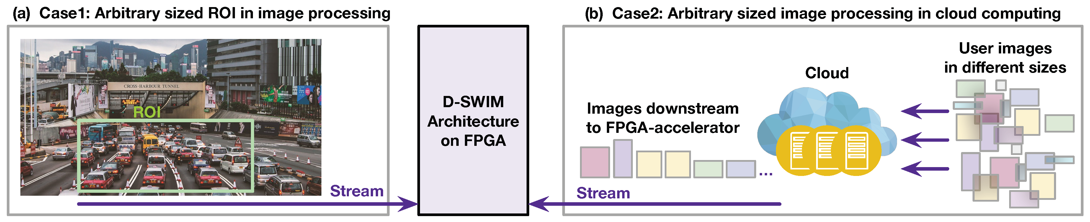
2.2. Demand on Arbitrary Sized Image Processing
In many real-world image processing scenarios, the size of the image is unpredictable before the system run-time. To demonstrate, Figure 2 presents two example cases.
Figure 2.
Motivation for arbitrary sized image processing: (a) user-defined Region of Interest (ROI) processing; (b) arbitrary sized image processing in cloud computing.
The first case is the Region of Interest (ROI) processing. As Figure 2a shows, the ROI is selected from the entire view of the image for analysis. This mechanism exists in most image applications that effectively reduce the computation workload. However, the ROI is defined by the end-user—hence, the size of ROI is unpredictable during the hardware design time. Furthermore, multiple ROIs may exist on the same view, such that the hardware is required to accommodate images of different sizes in processing one frame.
The second case presents how the arbitrary size image processing is also demanded in cloud computing. As Figure 2b shows, the users at the edge side upload images to the cloud for the computation-intensive applications (such as inference of deep learning, etc.). The cloud server sends the workload to the FPGA accelerator to reduce CPU processing time.
In both cases, the streaming architecture on FPGA is required to process arbitrary sized images. Furthermore, the working mode of hardware should be quickly switched for seamlessly processing the images. The conventional FPGA reconfiguration costs seconds to half a minute, which greatly reduces the system efficiency. Thus, we investigate a streaming architecture that can be rapidly programmed to process images in an arbitrary size.
2.3. Demand on Ultra-Fast Stream Processing
In previous works, the FPGA streaming architectures accept pixel streams with a throughput of one or two pixels per clock cycle (/) [5,7]. Due to the fast-growing bandwidth of peripherals, demand comes that FPGA should process multi-pixel blocks instead of independent pixels in each cycle. For instance,
- Near-storage processing: High-bandwidth memory (HBM) stacks multiple DRAM dies to achieve a bandwidth of 250 / [11]. Assuming the operating frequency of FPGA is 250 MHz, the max data rate of a FPGA input stream is 1000 /. For images with 1 byte per pixel, this translates into a pixel throughput of 1000 /.
- Near-sensor processing: The high-resolution image sensor represents a high pixel throughput. For instance, the up-to-date CMOS sensor Sony IMX253 is capable of capturing 68 frames per second, with a resolution of [12]. Thus, the minimum processing throughput on FPGA is 4 / ().
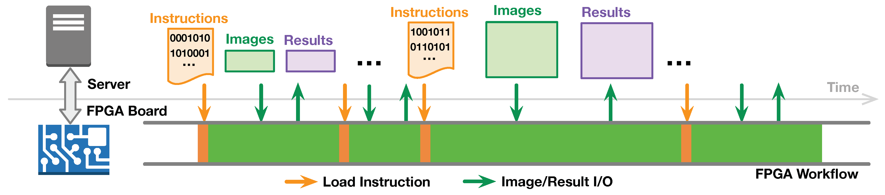
2.4. BRAM-Misalignment Challenge and SWIM Framework
An increase in processing throughput demands a more complex buffer that relies on the parallel pixel access using multi-pixel blocks. This, however, introduces potential memory alignment issues when utilizing BRAMs in the buffer design. An example in Figure 3a illustrates this problem, where the original image lines are sequenced into a high-throughput 1D pixel stream, and then clipped to pixel blocks by the serial-to-parallel hardware (deserializer) inside the FPGA. The image-processing logic accepts one pixel block in each cycle. Complication due to memory block misalignment arises when the pixel number of one image line (denoted as ) is not an integer multiple of the pixel number in an input block (). In this case, some of the blocks ended up encapsulating pixels from two image lines. As an example, in Figure 3a, we have and . Thus, , , , at the end of , , , contains 12, 8, and 4 pixels, respectively, that belong to the start of the next line. These pixels are labeled as remainder pixels in the example. As Figure 3b shows, the general pixel buffer is composed of multiple line buffers (LBs) and each LB stores an entire image line. The LB is implemented with one BRAM with a size of to fulfill the parallel pixel access. We annotated the BRAM index (n) and the address () in the diagram as to present the storage pattern. Note that the remainder of the pixels within the last block of each line will be stored in the following LB. Therefore, the storage of subsequent blocks may inherit an alignment offset relative to the BRAM boundary. For example, in Figure 3b, the last block of () contains 12 remainder pixels that are written to . To store the continuously in LB, two addresses of (,) are accessed. However, this behavior overwrites the pixels of stored in .
Figure 3.
(a) Shows that the image lines are sequenced into a stream and then clipped to multi-pixel blocks; FPGA accepts one block in each cycle. (b) Shows the general pixel buffer in which the BRAM-misalignment issue occurs. (c) Shows the SWIM buffer avoids the BRAM-misalignment using specific BRAM partition.
To address the misalignment issue, Wong et al. [9] proposed SWIM, a BRAM partition method for the pixel buffer design. With the same case, Figure 3c shows the SWIM buffer architecture and the pixel storage pattern. Each LB is composed of two BRAMs, and the width of the first BRAM is equal to the number of remainder pixels. For example, is composed of only one BRAM because there is no remainder pixel at the end of the previous line; is partitioned into and with widths of 12 and 4, respectively. Thus, the 12 remainder pixels in are stored at , and are stored separately at and . With this method, SWIM guarantees that the block storage is aligned to the BRAM boundary. Although the SWIM framework generates BRAM partition configurations that avoid the BRAM-misaligned access, the hardware configuration needs to be re-generated through FPGA synthesis flow for a different image width (). Even if the FPGA configuration files for different can be pre-generated before the run-time, the long disruption caused by FPGA reconfiguration for differently sized images significantly decreases the throughput.
3. Method
This section describes the Dynamic-SWIM (D-SWIM), a flexible buffer architecture that can be rapidly reconfigured to accommodate arbitrary sized images via instruction updates. First, an overview of the D-SWIM framework (hardware-, software-tools, and design parameters) is given; then, the hardware of D-SWIM is described. Subsequently, the control method of D-SWIM and the custom instruction-set are described, followed by the system working-flow illustration.
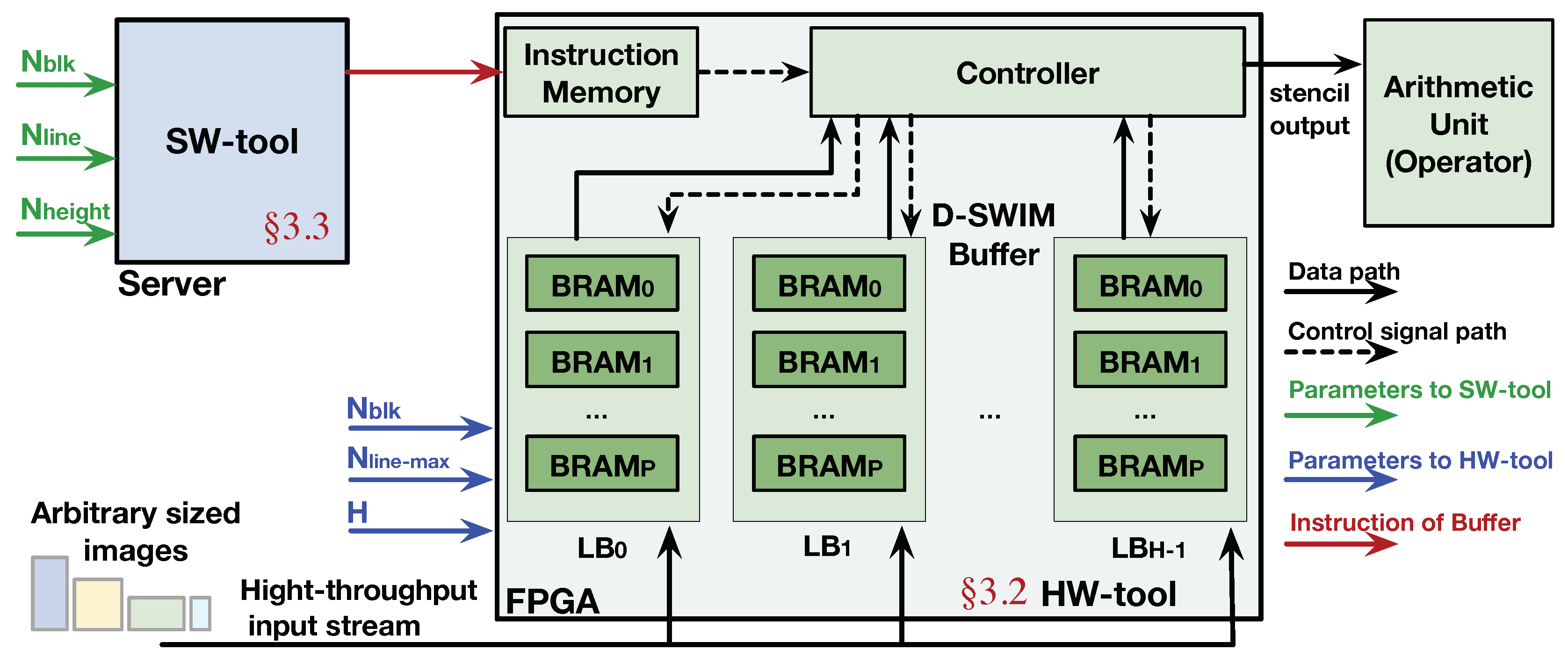
3.1. Framework Overview
As shown in Figure 4, the D-SWIM framework is composed of two parts: the software compilation tool, (SW tool), and hardware generation tool (HW tool). The HW tool generates hardware components following the D-SWIM method. Note that D-SWIM mainly optimizes the buffer hardware which is a general component of the streaming architecture, where specific arithmetic units (operators) are generated by FPGA synthesis tools without further optimization. According to the principle of stream processing in Figure 1, the of D-SWIM is composed of multiple line buffers (LBs), and the number of LB () is equal to the height of a 2D stencil (denoted as H). Details on the construction of LBs will be elaborated in Section 3.2. Inside the buffer hardware, the module provides the control signals to the underlying BRAMs to realize certain buffer behavior. Note that we employed an to provide the control words which can be pre-generated and loaded into the memory during run-time. By doing so, the D-SWIM hardware can accommodate the arbitrary image size by quickly switching the control words in the in a few cycles instead of performing FPGA reconfiguration. The SW tool generates the specific instruction words for the based on the pixel block size and image size, that will be described in Section 3.3.
Figure 4.
Overview of D-SWIM framework.
The design parameters used in D-SWIM are listed in Table 1. is the number of pixels in one block; is the number of pixels in one image line (image width), and is the image height; is the largest possible value of that decides the volume of the ; and H is the height of the 2D stencil pattern that determines the number of image lines stored in the buffer (number of LB). Table 1 also highlighted the use scope of each parameter. Note that the HW tool only invokes , , and H, which are independent to the image size.
Table 1.
Design parameters in D-SWIM framework.
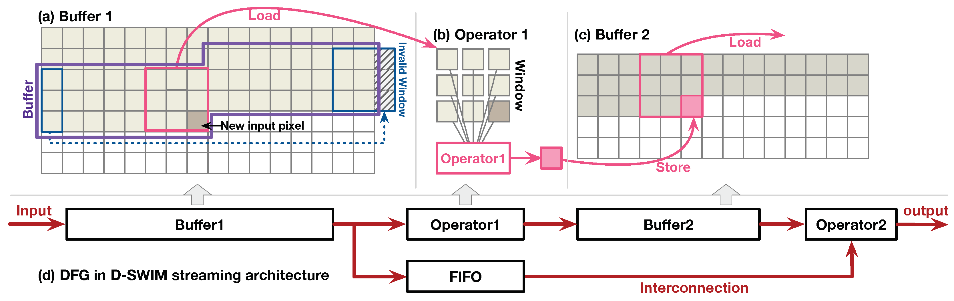
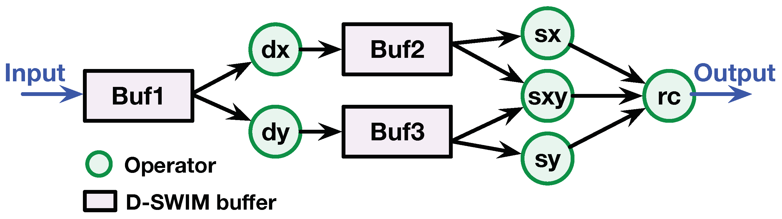
3.2. Buffer Architecture in D-SWIM
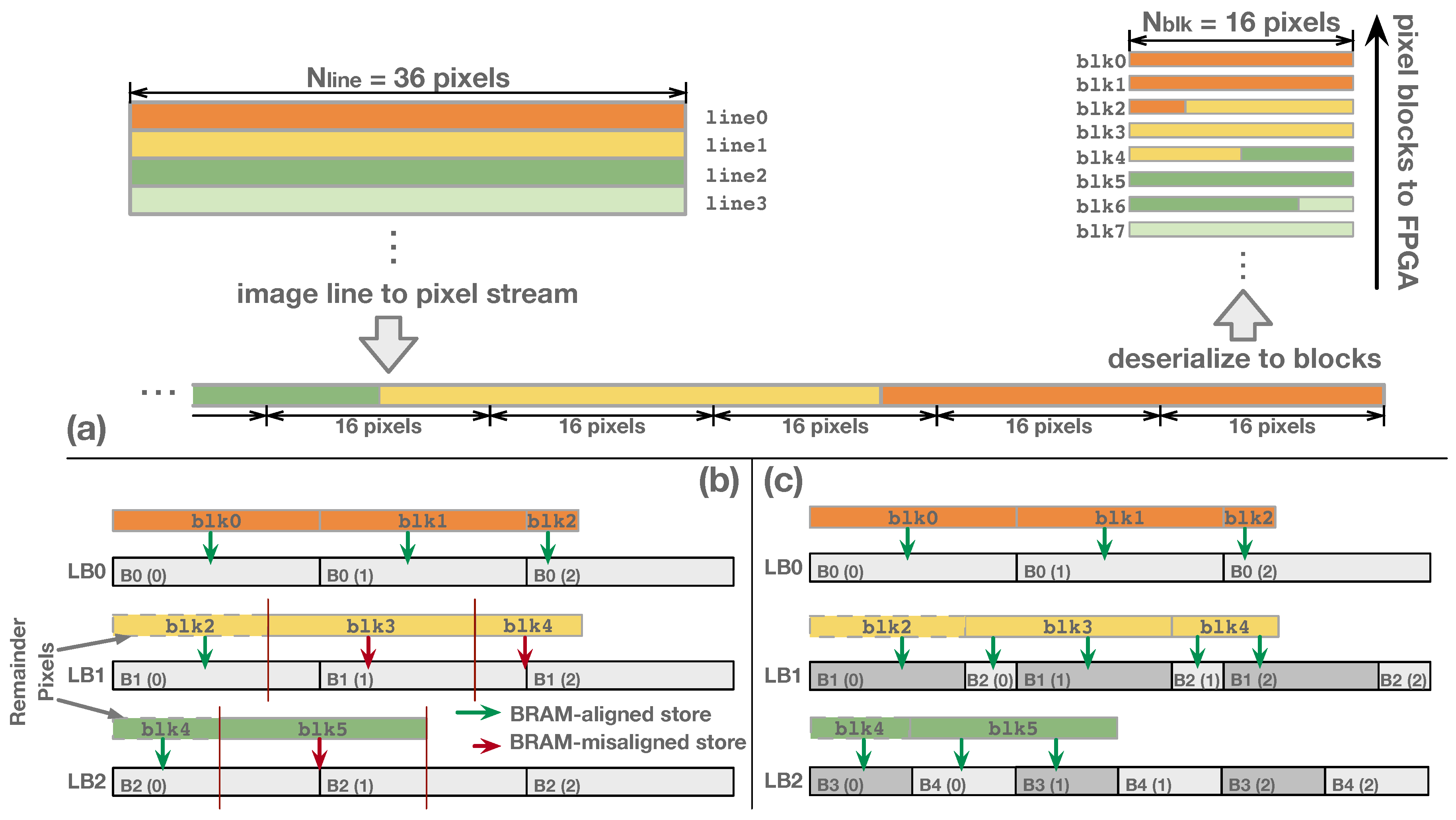
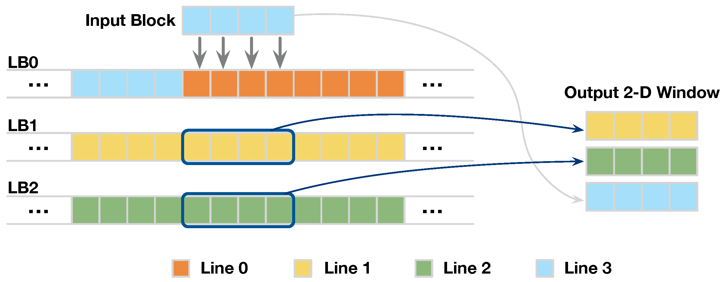
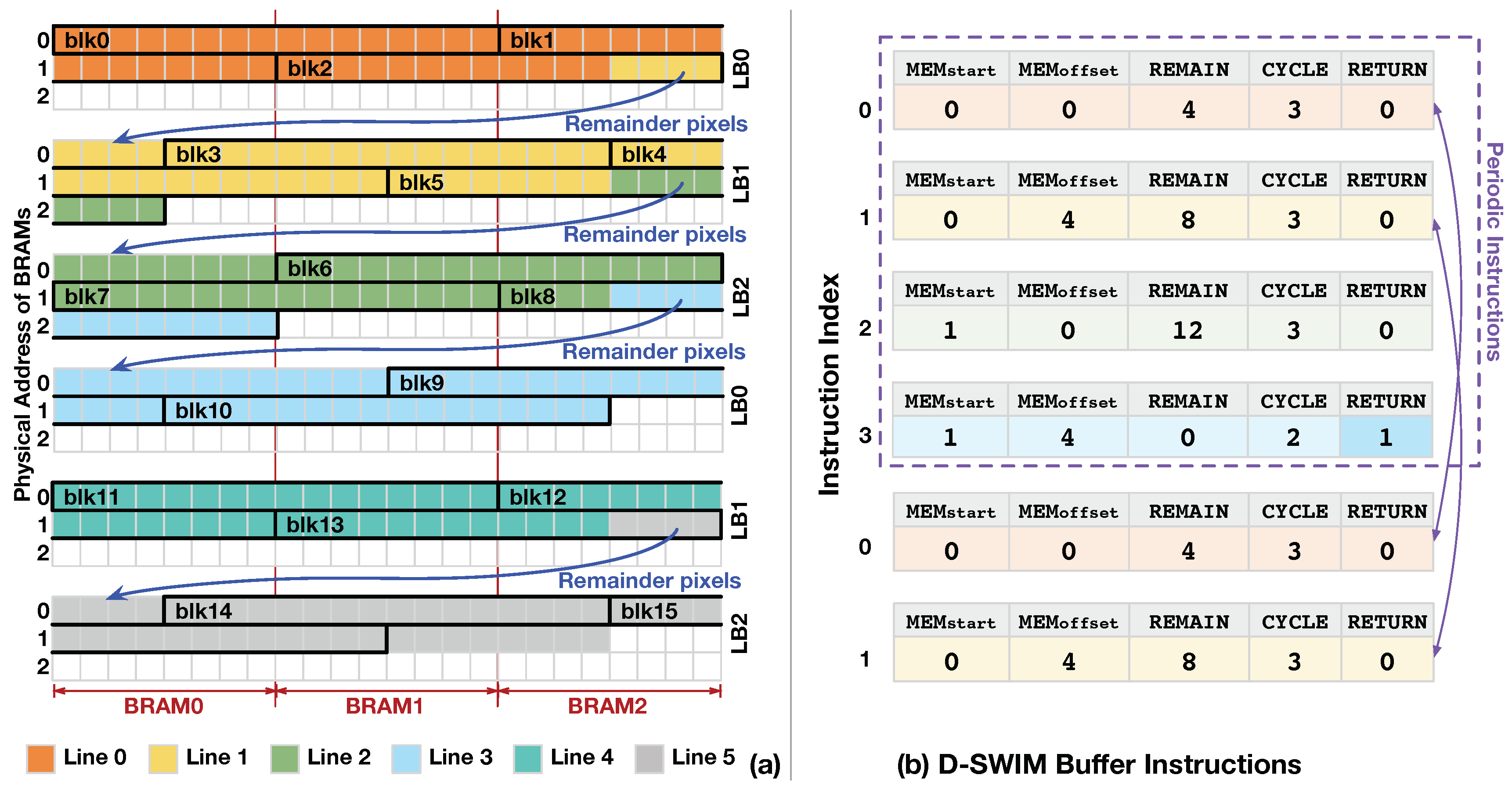
3.2.1. BRAM Organization of Line Buffer
Similarly to SWIM, the D-SWIM buffer is composed of BRAM that saves the FPGA hardware resource and avoids the complex routing requirement. This section describes the BRAM-centric technique for the D-SWIM buffer construction.
BRAM Configuration: D-SWIM directly employs the BRAM primitive for the buffer. The port width of BRAM can be configured. To accommodate the parallel pixels access of the input block and fully utilize the BRAM bandwidth, we configured all the BRAMs to a port width of 64 bits in the simple dual-port (SDP) mode. Note that the real maximum port width is 72 bits, whereas only 64 bits are under the control of the byte-wise write-enabling signal. The conventional usage of BRAM considers all bits in one address as an element in memory access. As Figure 5a shows, the store of the input block should align to the BRAM boundary—otherwise, the misaligned store will overwrite the other bits in the same address. To avoid interference between two consecutive blocks which is misaligned with the BRAM, we used the BRAM primitive instantiation within Xilinx Vivado that provides a byte-wise write-enable signal [13]. For instance, in Figure 5b, the input block (8 pixels, 8 bits/pixel) is misaligned to the BRAM boundary because the 4 pixels in the head of are stored along with the previous block. With the byte-wise write enable, the specific control bits in and are set to indicate the store positions of the incoming 8 pixels and the 4 remainder pixels ahead will not be overwritten. In summary, with the BRAM primitive instantiation, the controlling of the pixel-block store becomes more fine-grained. Furthermore, the write enable signal can be changed in the FPGA run-time such that the LB accommodates arbitrary writing offset introduced by the remainder pixels.
Figure 5.
(a) shows LB write behavior with conventional BRAM usage. (b) shows LB write behavior with the byte-wise write enable signal using BRAM primitive instantiation.
Number of BRAM in LB: The number of BRAM invoked by one LB (denoted as ) is determined by the system parameters in Table 1. D-SWIM targets minimizing the BRAM consumption under the constraints in Equation (1). Firstly, the capacity of the LB should be larger than . Secondly, the overall port width of the LB should be large enough to tackle the pixel block and ensure that only one address in each BRAM will be accessed in one cycle, such as the minimum is 2 in the Figure 5b case. Otherwise, two addresses of will be accessed in the same cycle that violates the port limitation of BRAM in the SDP mode.
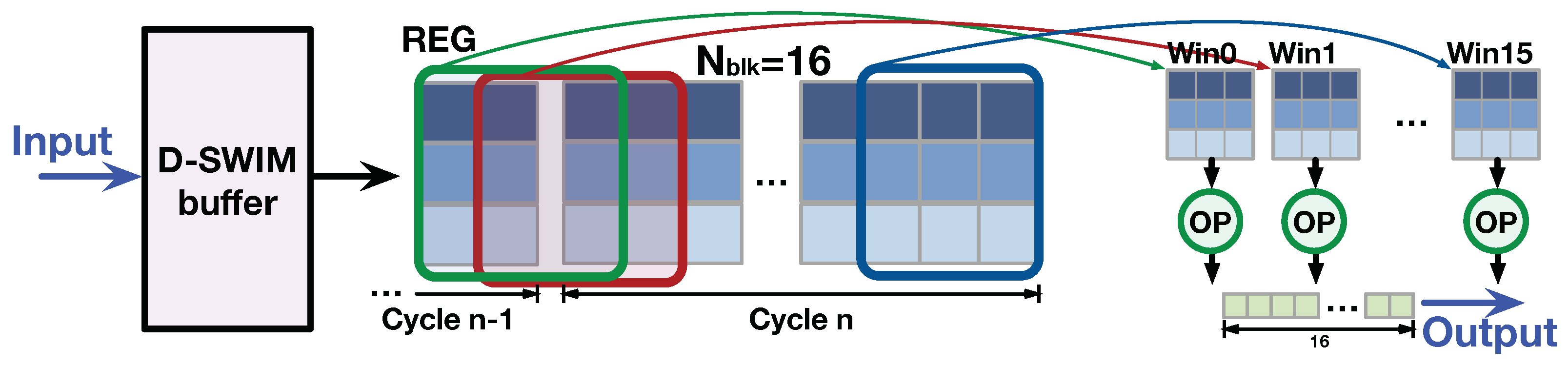
3.2.2. Line-Rolling Behavior of Line Buffers
The buffer in D-SWIM stores and loads the successive image lines with the line-rolling mechanism. To demonstrate the line-rolling clearly, we show an example with in Figure 6. At the beginning, the - are stored in the -, respectively. When the buffer receives the incoming , the input block is stored in and replaces the old pixels of which is no longer needed. With this line-rolling mechanism, the successive image lines are stored in all in a cyclic manner.
Figure 6.
Example of buffer load and store with the line-rolling behavior.
Meanwhile, the buffer outputs a 2D window including pixels from H image lines, and the blocks in the window are spatially aligned to the input block. As Figure 6 shows, the first two blocks of the output window are loaded from the , while the last one is directly sourced from the input block. Because the output blocks are aligned in the vertical direction, the 2D windows are continuous in the horizontal direction. Thus, the output 2D windows cover all the pixels required by an arbitrary 2D pattern with a height of H.
3.3. Line Buffer Access Pattern and Control Instruction
3.3.1. Access Pattern of Line Buffer
Since the image lines are vertically aligned in the LBs, the load addresses are synchronized to the store address of the LB which accepts the input block. We use an example in Figure 7 to demonstrate the pixel access pattern in the underlying BRAMs. The parameters, , and H are set to , respectively in the example. With the D-SWIM method, we set 3 LBs () in the streaming architecture, and each LB is composed of 3 BRAMs (). The store position of input blocks (-) are highlighted in the LBs. In each cycle, one BRAM address is accessed at most to ensure that the previous constraint of BRAM port is not violated. For the blocks that are not aligned to the BRAM boundary, such as -, a byte-wise write enable signal was used to make sure only the positions marked by the enable signal were updated and the other pixels in the same address are not overwritten. Note that the remainder pixels in the last block of each line are duplicated and stored at the beginning of the successive LB. For example, contains 4 pixels of (). Thus, these pixels are written to both of and of , concurrently.
Figure 7.
(a) shows an example of the block storage pattern with parameters , , and . (b) shows the buffer instruction list for achieving the access pattern in (a).
Note that from the , the storage pattern in LBs will be the same as that from . This is because the values of in continuous lines show a periodic pattern, and the period is determined by and . The period measured in clock cycle () or in image line () is given by Equation (3).
where LCM is the least common multiple. In addition, of line l (denoted as ) is calculated as Equation (4).
where l is the index of the line. With the equations above, the buffer access pattern is deterministic. Thus, in the Figure 7 example, every 4 lines have the same LB storage pattern, and the value of shows a periodic pattern of .
3.3.2. Control Code Generation
To perform the buffer store and load with the proposed access pattern, D-SWIM adopts customized instructions along with hardware logic to control the LBs. The BRAM control signals inside each LB are given by the instruction codes and decode logic, and the line-rolling behavior (store block/load block) is controlled by the hardware logic. The instruction codes for a specific image size were generated and loaded into the before run-time. The instruction-based control method has two key benefits: firstly, it saves hardware logic for control signal generation; and secondly, the content in the can be rapidly switched for processing differently sized images. Note that each instruction manages the buffer behavior over multiple cycles corresponding to one image line.
As Table 2 listed, the customized instruction is composed of five sections, and each of them is translated into specific BRAM control signals by the control logic. Because an arbitrary number of remainder pixels () may exist ahead of the first block of a line (line-initial block), we set section to give the BRAM index from which to store the line-initial block. Furthermore, since the block access may not be aligned to the BRAM boundary, the offset position inside a BRAM is given by section . In the D-SWIM design, we constrained to be an integer multiple of the BRAM width (). Thus, all pixel blocks in one image line have the same offset inside a BRAM, which is given by . This constraint leads to a regular storage pattern and reduces the hardware logic usage for control signal generation. Section gives the value of , which represents the number of pixels in the last block of a line that overflows into the successive line, and they are duplicated and stored in the next LB. Section gives the number of blocks in the line, which indicates the cycle number of the control period for the current instruction code. In addition, determines the interval period of fetching a new instruction.
Table 2.
Sections of the customized instruction for D-SWIM architecture.
The periodic access pattern of continuous image lines presented in Equation (3) enables instruction reuse. For instance, is 4 in Figure 7a; thus, only four instructions are needed. To reuse the instruction periodically, section gives the flag to reset the instruction-fetch address and restart a new period of the access pattern. The periodic reuse of control code saves the instruction memory and reduces time delay caused by instruction reloading while switching the image size. Theoretically, the maximum possible number of instruction is .
Algorithm 1 gives the instruction generation flow in D-SWIM’s SW-tool. Each iteration of the program calculates five sections and then assembles the instruction to binary codes. The iteration continues till (value of section) gets to zero. In the last instruction of the list, is set to 1, that leads to re-execution of the entire instruction list. For instance, Figure 7b gives the instruction code for each image line in Figure 7a, which is generated by Algorithm 1. For , the line-initial block starts from without pixel offset. Thus, and are 0. It takes 3 blocks to fulfill the , and the last block contains 4 pixels belonging to the following . Thus and is equal to 4 and 3, respectively. Algorithm 1 starts with an initial state that all variables are set to 0, and input parameters , , and are set to 44, 16, and 64, respectively. In the loop iteration, the variables are calculated sequentially, and they are corresponding to the value of each instruction section for . Then, the values of five sections are assembled into the and appended to the instruction list. Following the , the line-initial block of starts from of with a inner-BRAM offset of 4 pixels, which can be translated to and in , respectively. The other sections are conducted using the same manner as . In particular, only 2 blocks are required to fulfill ( in ), because there are 12 remainder pixels contained in the last block of . The does not contain remainder pixels, that results in pixel blocks from which perform the same storage pattern with that of blocks from . Therefore, in the algorithm loop iteration for , variable is set to 1, and the loop stops. Then, the algorithm outputs the instruction list (-) that can be periodically executed in processing continuous image lines.
| Algorithm 1: Instruction Generation Algorithm in D-SWIM Streaming Architecture |
| Input: Application parameters: , Hardware information: Output: Instruction code: ; = 0; = 0; = 0; = 0;
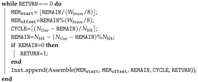
 ![]() return |
3.4. Run-Time Dynamic Programming for Arbitrary-Sized Image
With the specific instruction set, the D-SWIM buffer can be rapidly re-programmed for processing arbitrary sized images. Figure 8 demonstrates the system workflow on both the FPGA and the server. The server obtains the images from users and prepares the D-SWIM instruction list for the image size. Due to the low complexity of the instruction generator in Algorithm 1, the server generates the instruction list online and then writes it to the of D-SWIM at the FPGA side. Besides the instruction, the server also sends the value of image height () to the control register in D-SWIM that determines the life-cycle of the instruction list. Subsequently, the server sends the corresponding image to the FPGA and obtains the computational results in a continuous data stream. Note that the communication latency is hidden in the fully pipelined workflow. Thus, the image computation logic on FPGA only stalls for a brief period of time during instruction loading.
Figure 8.
D-SWIM workflow with dynamic programming for arbitrary sized image processing.
4. Logic Implementation of D-SWIM
This section explains the detailed implementation of the underlying logic hardware of D-SWIM. Note that the main focus here is a universal buffer design for image-processing-based streaming architectures on modern FPGA architectures. Further optimizations may apply to specific applications on FPGA architectures, but it is outside the scope of this section.
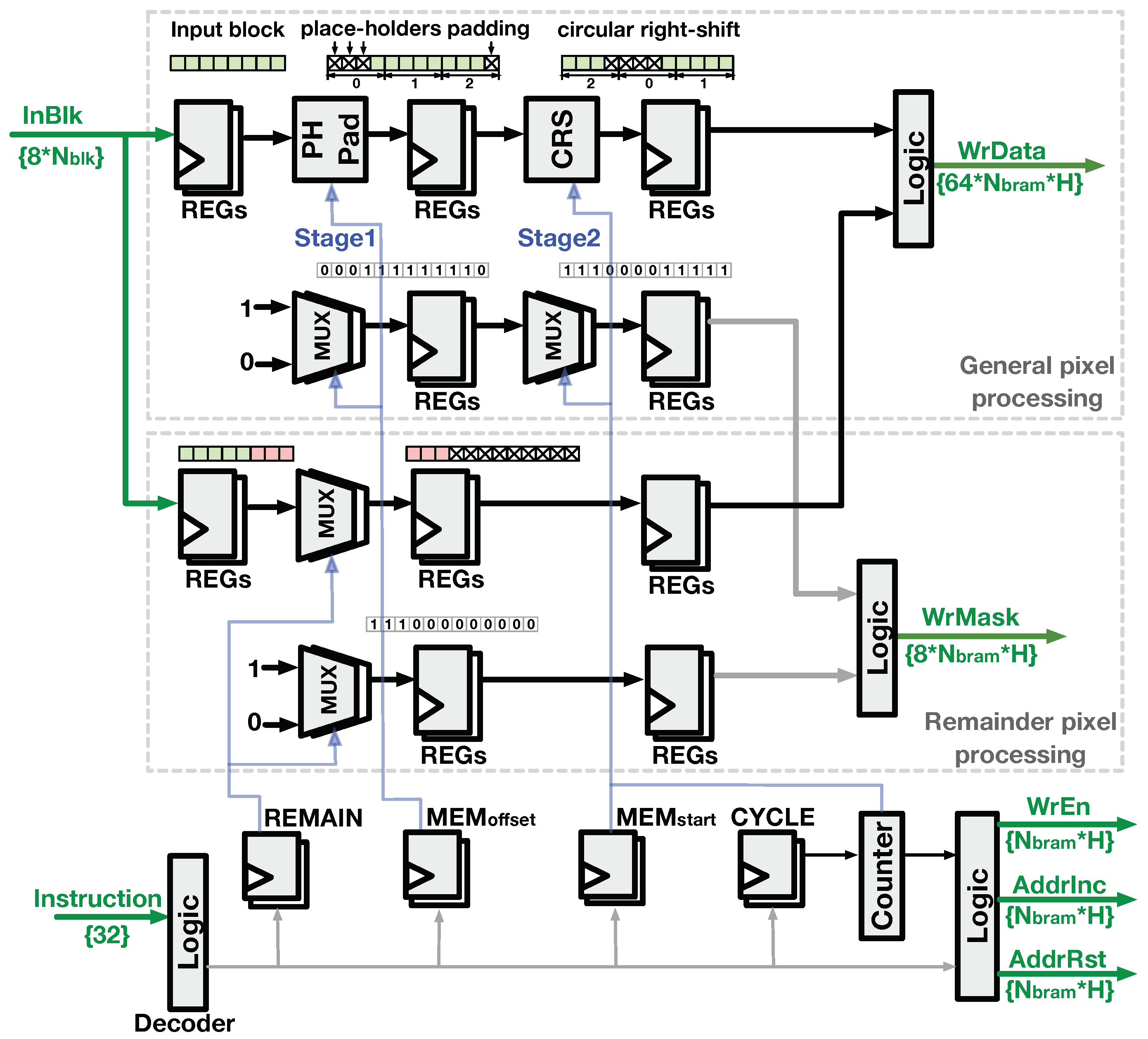
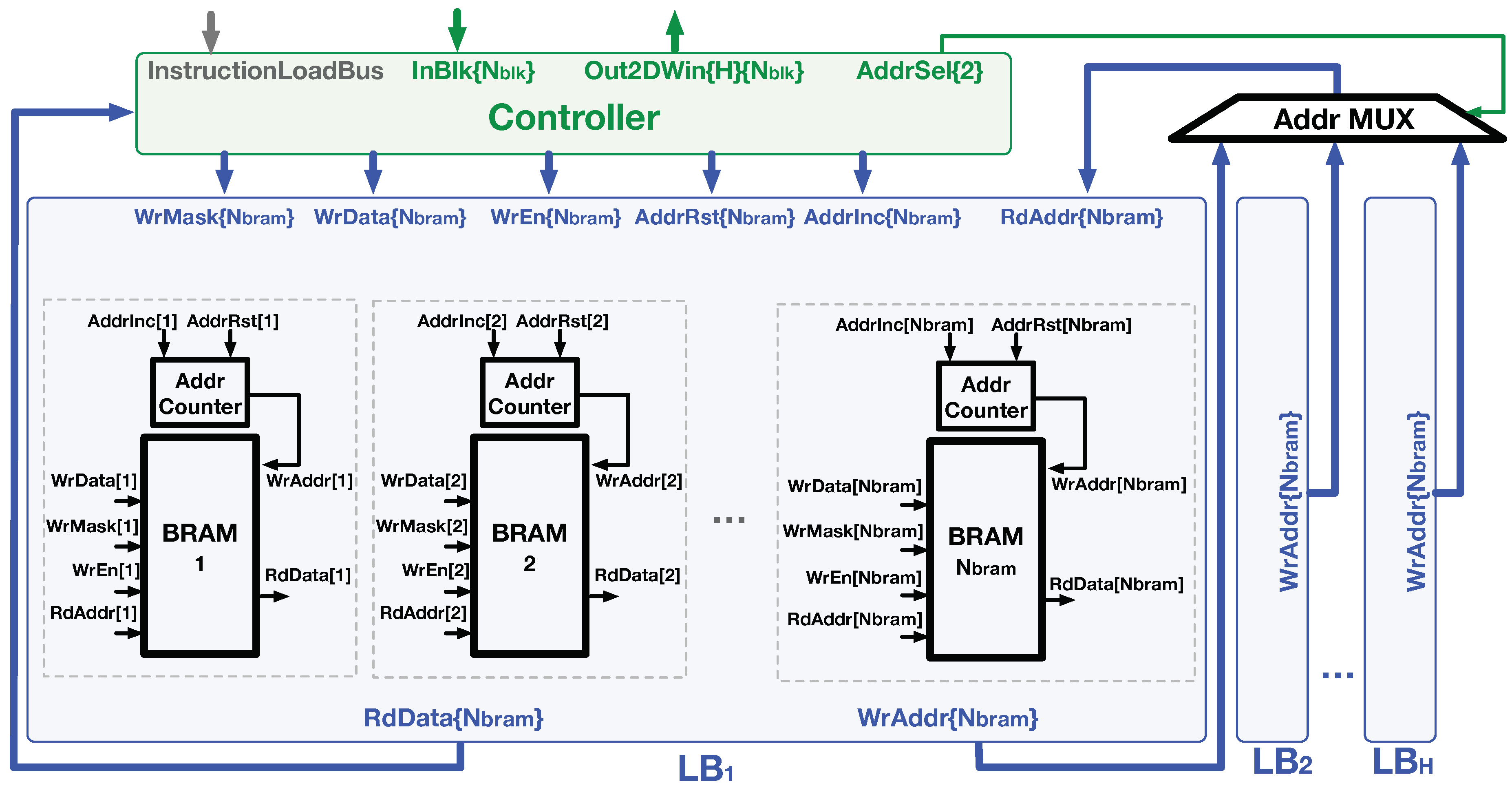
4.1. Logic of Line Buffer
Figure 9 shows the hardware composition of the Line Buffer () and the related control signals from the module. Each LB is composed of BRAMs and the associated control logic. According to the LB access pattern described in Section 3.3, the BRAM addressing pattern is sequential. Thus, we employed an module to each BRAM to manage the write address. The accepts the and signals from the that determines whether to increase the address register by one or reset it to zero, respectively. The other signals related to the block store process, including , , and , were generated by the and directly connected to the BRAM primitives. Note that we annotate the width of each signal bus in the brace following the signal name in Figure 9.
Figure 9.
The D-SWIM buffer is composed of and . Each BRAM in the LB is equipped with an to manage the write address. It performs address incrementation or reset according to the signal on the controller bus. The allows the write addresses to be broadcasted during a block write operation of a specific LB as the read addresses of the other LBs for block loading.
According to the line-rolling buffer access behavior, the read addresses of multiple LBs were synchronized to the write address of the LB which stores the input block. In the logic design, the from were sent to a , and the selected the proper value as the signal of all LBs under the control of the signal.
4.2. Logic of Controller
The performs three functions in D-SWIM: (1) decode the instruction word to the control signals of each LB; (2) transform the input pixel block () to the proper storage pattern as the signal of the BRAMs; (3) transform the pixels loaded from LBs to the certain 2D window required by the operators (). Thus, the buffer-write and buffer-read logic are implemented independently as follows.
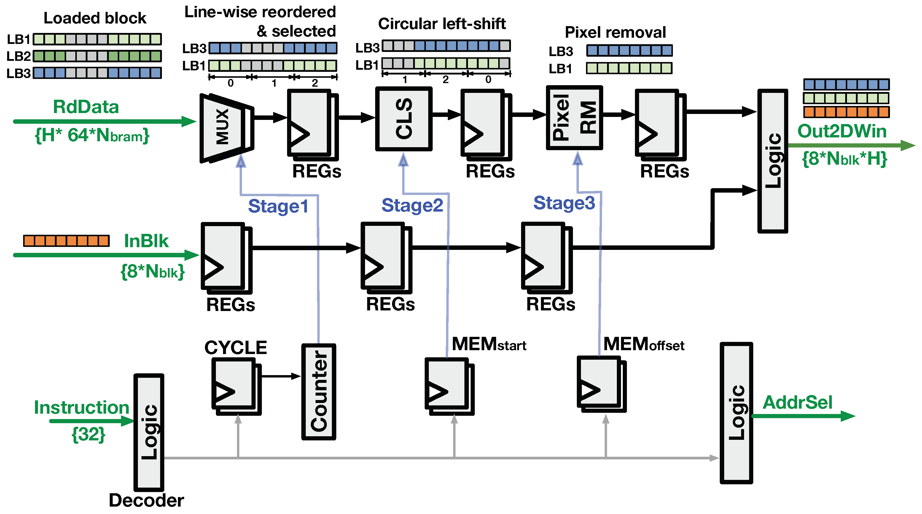
4.2.1. Buffer-Write Logic
In the D-SWIM design, the length of input block () is larger than the width of LB. Thus, the buffer-write logic extends the signal to the same width of LB in a certain pattern, and the BRAM byte-wise write enable signal () is generated concurrently. As Figure 10 shows, two stages exist in the signal generation. In the first stage, place-holding bytes (cross marked in Figure 10) are padded at the beginning and the end of the input block. By doing so, the padded block has the same width as the LB. The number of place-holders at the start of the block is equal to in the instruction word. Thus, the hardware in this stage is controlled by the corresponding register decoded from the instruction. In the second stage, the pixels from the first stage are rearranged by a circular right-shift (CRS) operator. The shift distance is an integer multiple of the BRAM width, and it is given by in the instruction that ensures the pixel-block storage starts from the proper BRAM in the LB. Note that the pattern of place-holder padding is fixed for blocks in the entire image line, but the shift distance in the second stage changes for every block. Thus, the hardware in the second stage is controlled by the and a run-time which provides the input block index of one image line. Along with the signal, the signal is generated in a similar manner. After the two-stage processing, a set of binary flags are generated, where 0 corresponds to the positions of the place-holders in and 1 indicates that the BRAM byte position will be overwritten by the value in .
Figure 10.
Buffer-write logic.
In particular, when the input block exceeds the end of the image line, the logic stores the remainder pixels belonging to the next image line to the beginning of the next LB concurrently, where specific logics are set to process these remainder pixels. Because the number of remainder pixels is provided by the section in the instruction, the in the logic separates remain pixels (red pixels in Figure 10) and pads place-holders in the tail as the signal of the next LB, while the signal with ones at the beginning of the binary set is generated. Subsequently, the and signals from the circuits for general pixels and remainder pixels are concatenated as the output bus of the . Other buffer-write related signals, , , and , were generated concurrently by the and specific logics.
4.2.2. Buffer-Read Logic
As introduced previously, the BRAM read address was synchronized to the write address of the being written. Thus, the generates the signal to indicate the LB index that stores the input block. The loaded from multiple LBs are processed by the buffer-read logic to form the output 2D pixel window () from multiple image lines. The buffer-read logic reverses transformation performed during the buffer-write process, and the circuit is shown in Figure 11. The logic contains three stages to transform the into . The first stage performs line-wise reordering that changes the line-order of the LBs’ output blocks to the spatial order of the image. As per the line-rolling behavior in Figure 6, - blocks of are read from the LBs, and the last block is directly sourced from with delay logic. The second stage performs a circular left-shift (CLS) which reorders the pixels from different BRAMs. The third stage removes several pixels at the beginning and the end of results from the previous stage, which ensures the output blocks are spatially aligned to the . Subsequently, the pixel blocks after the three-stage processing are concatenated with the delayed to construct the .
Figure 11.
Buffer-read logic.
5. Evaluation
This section describes the experimental setup for evaluating the D-SWIM implementation. In the evaluation, we compare this work with SWIM in terms of hardware resource usage, timing, and power consumption on FPGA. Subsequently, we evaluate the D-SWIM workflow with dynamic programming for continuously processing images in different sizes. Furthermore, we present D-SWIM based hardware architectures for two real-world image applications (2D-Convolution and Harris Corner Detector). The implementations are compared to streaming architectures in prior works.
5.1. Experiment Setup and Evaluation Metric
The hardware generator of D-SWIM was realized using Verilog RTL and implemented with Xilinx Vivado. Our selected target FPGA device was Xilinx-XC7VX690, where the tool synthesizes the Verilog into logic circuits and generates FPGA-specific mapping. Meanwhile, it also gives the resource utilization and timing performance, which are generally employed as the evaluation metrics of FPGA implementation. The resource utilization can be broken down into four FPGA building-blocks: the look-up table (LUT), Flip-Flop Register (REG), BRAM, and DSP. On the timing performance, the worst negative slack (WNS) of the critical path is given by Vivado and can be translated to the maximum operating frequency (). The vendor tool gives the power consumption of the D-SWIM module as well. Besides the hardware tools, we implemented the D-SWIM instruction generator on the server to provide the control codes for any given image width () and block size ().
5.2. Evaluation of Buffer Hardware
We evaluated the buffer design in D-SWIM and compared it with the previous work of SWIM, which tackles the similar BRAM-misalignment issue for the multi-pixel block but only supports static image sizes that are pre-defined before FPGA synthesis. In the experiment, we configure the SWIM and D-SWIM with different parameter sets for a complete evaluation. As Table 3 shows, the parameters (, H, and ) are set to different values, and the implementation results are listed. In Configurations 1–6, we set the image width () to arbitrary values. The window height (H) was set to 3 or 5, which are frequently used in image applications. The pixel number of one input block () was set to . Note that in the SWIM method, the number of LB () was deduced by and ; thus, it may exceed H, whereas is equal to H in D-SWIM. The optimization technique of multi-pass BRAM partitioning in SWIM was also invoked to reduced , and the corresponding results are shown in the SWIM-2pass column of Table 3.
Table 3.
Buffer resource consumption in SWIM and D-SWIM.
5.2.1. Resource Evaluation
Table 3 lists the resource consumption of LUT, REG, and BRAM for different buffer schemes. Note that the results of D-SWIM and SWIM-2pass schemes are compared, and the ratio values of D-SWIM to SWIM-2pass are listed in the parenthesis of the D-SWIM column. In Configuration 1, D-SWIM consumes and more LUT and REG than that in SWIM. However, the BRAM consumption in D-SWIM is less—this is because is 4 in SWIM as 4 lines compose a BRAM-partition period, but this issue does not exist in D-SWIM. When is set to 16, as per Configuration 2, of SWIM increases to 8, which consumes more logic and BRAMs than D-SWIM. Although the 2-pass optimization halves the , the BRAM cost in SWIM is 16, which is times that of 9 in D-SWIM. SWIM costs more BRAMs of specific widths to compose the LB, whereas D-SWIM sets all BRAM ports to the maximum width, which fully utilizes the bandwidth and reduces the resource. Note that the D-SWIM buffer accommodates arbitrary image width, and configurations use different values but identical H and (e.g., Configuration 2 and Configuration 3) share the same hardware via dynamic programming. In Configurations 5–6 where H is 5, D-SWIM’s consumptions of both logic and BRAM are less than SWIM. D-SWIM saves LUT, REG, and BRAM compared with SWIM-2pass in Configuration 6. With Configuration 6, the of SWIM is 8, which costs more logic on the line-selection multiplexer.
We also investigate the impact of parameters on the resource consumption in the D-SWIM scheme. Comparing the results in Configurations 1–4, we note that greatly affects the logic and BRAM resources. This is because a larger requires more complex multiplexers for pixel-block manipulation. Note that H also affects the hardware (comparing Configuration 3 to Configuration 5) because a larger H costs more LUTs for the line-selecting multiplexer and more REGs on the temporary pixel-storage.
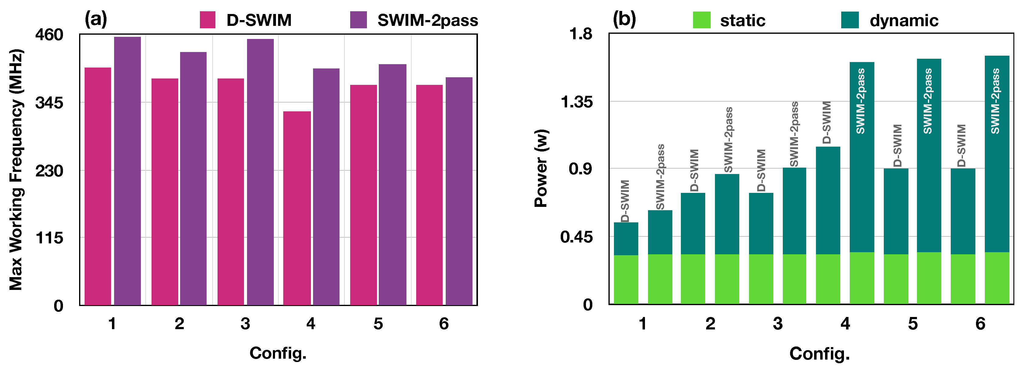
5.2.2. Timing and Power Evaluation
In addition to the hardware resource usage, timing performance and power consumption were also evaluated. The results of the post place-and-route design were obtained from the vendor tools (Xilinx Vivado) and presented in Figure 12, where (a) is the with different configurations in Table 3 and (b) is the power consumption. Compared with SWIM, the D-SWIM design slightly decreases the . This is because the multi-stage logics for dynamic controlling lengthen the critical path. We selected the proper pipeline stage as described in Section 4, while trading the and resource overhead in further pipelining. We observed that is a significant factor to the . In Configurations 1–6, the worst is with Configuration 4 in which is 32.
Figure 12.
(a) shows the of D-SWIM and SWIM designs with the configurations in Table 3. (b) shows the power consumption of D-SWIM and SWIM, with the breakdown of static and dynamic power.
Figure 12b presents the power consumption of buffer modules with SWIM and D-SWIM design methods. Each power bar is composed of two portions that represent static power (lighter part) and dynamic power (darker part). Apparently, SWIM and D-SWIM have identical static power with all configurations, but D-SWIM performs better in the dynamic power aspect. This is mainly due to fewer LBs () used in the D-SWIM case, which leads to less BRAM usage. For example, with Configuration 5, SWIM consumes BRAMs of that in D-SWIM; thus, the dynamic power is increased proportionally. Compared with SWIM, the D-SWIM buffer saves up to power consumption in the case of Configuration 6.
5.3. Evaluation of Dynamic Programming in D-SWIM
The dynamic programming described in Section 3.4 contributes to the ability of rapid context-switching for arbitrary sized images. We evaluated the D-SWIM system with the workload containing images in different sizes. Table 4 lists the period of computation and dynamic programming for one image. The independent variables are image size and (input throughput), which affects the measured periods. The values were measured in clock cycles. However, for direct comparison, they were converted to the numbers in micro-seconds with an operating frequency of 350 . The proportion column gives the ratio of the programming period to the entire working period (programming period + computation period). The overhead of dynamic programming in D-SWIM is significantly less than in most cases, and the context-switching can be regarded as seamless.
Table 4.
Time period of dynamic programming of D-SWIM and partial reconfiguration of SWIM.
In contrast, while employing the SWIM buffer for the same workload, a FPGA reconfiguration is required to switch the specific hardware corresponding to the size of the input image. The average period for reconfiguring the entire FPGA device (Xilinx-XC7VX690) is 20 s. For a fair comparison, we listed the time period for the partial reconfiguration technique [14], which reduces the reconfiguration time to the order of milliseconds via programming only a portion of the FPGA. Similarly, we obtained the proportion of FPGA reconfiguration time based on the image-processing period. Assuming the SWIM hardware is reconfigured for each image, the results show that the FPGA performs reconfiguration in over of the entire working period. This means that the FPGA spends the most time on reconfiguration rather than actual image processing, causing a huge reduction in processing throughput.
5.4. Case Study of Image Processing with D-SWIM
With the D-SWIM buffer, an architecture for a specific image application can be easily constructed. This section presents D-SWIM-based architectures for two real-world image applications and their performance study.
To evaluate the practicability of D-SWIM in real applications, we compare the D-SWIM designs with similar streaming architectures for image processing [7,10]. In prior studies, Reiche et al. [7] improved the image-processing framework to generate effective High-level Synthesis (HLS) codes for FPGA with a specific memory architecture, and Özkan et al. [10] optimized the OpenCL framework of Intel (Altera) FPGA to a domain-specific language (DSL) for image processing. These works are widely accepted by the community, and were developed based on the latest tools from the industry and academia. Thus, we consider these two as the state-of-the-art works for comparison.
5.4.1. Conv2D
2D convolution (Conv2D) is a popular operation for image feature extraction. Figure 1 shows a typical Conv2D operation with convolutional kernels. Pixels in a kernel-sized window were fetched and multiplied to the kernel weights and then accumulated to the Conv2D result. The subsequent operation moves the window 1 pixel to the right, and performs the same arithmetic. In the high-throughput scenario of D-SWIM, multiple overlapped windows are processed in the same clock cycle. Thus, the logic components are connected as Figure 13. In every clock cycle, the buffer output pixel block has a height of H, and width of . The pixels were directly delivered to the parallel operators () which performed the MACC operation. The results of were concatenated to the output block. Note that there are windows, such as and , in Figure 13, containing pixels from two consecutive output blocks of the buffer. Thus, we set registers to store the last pixel-columns of the previous cycle to construct these windows.
Figure 13.
D-SWIM-based architecture for Conv2D ( window).
Following the architecture above, we implemented the Conv2D with and . For a fair comparison, the hardware of was simply implemented with naïve RTL with a pre-defined pipeline stage. The implementation results are listed in Table 5. We name the works in [7,10] Design2 and Design1, respectively, in the following content. The devices adopted in each work have been listed as a reference. Note that the size of BRAM in Intel FPGA is 20 Kbits, whereas it is 36 Kbits in Xilinx FPGA. represents the hardware throughput (pixel/cycle). Meanwhile, the of each design has been given, and we obtained the system pixel throughput (giga pixel per second (GPPS)) by .
Table 5.
Hardware resource consumption and throughput in a Conv2D implementation.
Because D-SWIM and Design1–2 have different throughputs, it was unfair to compare the resource number in Table 5 directly. Thus, we obtained the hardware efficiency of FPGA logic (LUT and REG) with Equation (5). Comparing with the highest-throughput design (Design1), the hardware efficiency of D-SWIM is and in LUT and REG, respectively. Comparing with the smallest design (Design2), D-SWIM also achieves competitive hardware efficiency. Note that Design2 achieves higher hardware efficiency on LUT, as it has traded off throughput severely for simpler logic. Moreover, it does not consider the issues in the multi-pixel input scenario (such as BRAM-misalignment), which allows further reduction in overall hardware usage.
5.4.2. Harris Corner (HC) Detector
The Harris Corner (HC) detector [15] is commonly used in computer vision applications that detects the corner position for feature matching. The HC operator swaps the window (e.g., pixels in the benchmark) on the image and determines if the window contains a corner pattern. The HC algorithm on each window is listed in Equation (6). Firstly, HC obtains the gradient matrix , where is the intensity value of the pixel inside the window; and are the intensity derivative in the horizontal and vertical axes, respectively. Secondly, R was calculated to estimate the eigenvalue of , where k is a constant of –, and det and trace calculates the determinant and trace of the matrix, respectively. If the value of R is larger than the threshold, the current window contains the corner pattern.
Figure 14 demonstrates the D-SWIM-based architecture for HC. This streaming architecture is composed of a buffer (rectangular shape), operator (circular shape), and interconnections. Note that the derivative calculation in different axes can be realized by a Conv2D operation with the Sobel kernels. We used a Sobel kernel in the example, and the operators are denoted as and for the two axes. The derivative results (, ) were stored in and because they were accessed with a 2D window pattern in the subsequent operations. The , , and operators perform the element-wise multiplication and accumulate the values in the window. After is obtained, operator calculates the R in Equation (6) and compares it with the threshold to determine whether the window contains a corner or not.
Figure 14.
D-SWIM-based architecture for HC detector ( window).
The evaluation method of HC is the same as the Conv2D case. Table 6 shows the implementation results of D-SWIM and Design1–2. In the HC case, the D-SWIM-based design achieves both the highest throughput and the best hardware efficiency. Comparing with the superior design (Design1), D-SWIM increases the throughput to . Furthermore, with D-SWIM, the efficiency of LUT and REG is and that in prior studies.
Table 6.
Hardware resource consumption and throughput in HC detector implementation.
6. Conclusions
This work has presented D-SWIM, a dynamic programmable line buffer microarchitecture for arbitrary sized streaming image processing on FPGAs. The D-SWIM architecture facilitates high-throughput realignment of multi-pixel blocks into line buffers suitable for further streaming image processing. In addition, through a rapid instruction code update, D-SWIM allows for the size of line buffers to adjust dynamically to accommodate varying size requirements of the application during run time. Compared to prior studies where SWIM can only work on a predetermined image size, D-SWIM achieves dynamic programmability for varying image sizes with a slight logic resource overhead. In our experiment, the D-SWIM buffer reached a maximum operating frequency of and saved BRAM resources up to that contributed to a power consumption reduction of . When compared to other state-of-the-art FPGA-based streaming architectures using two real-world image applications as benchmarks, D-SWIM contributes to a significant hardware efficiency improvement of in LUT and in REG. For the benchmark cases, the D-SWIM based design reaches a pixel throughput of GPPS when 16 pixels are input every cycle.
As more applications domain begin to take advantage of vision-based intelligence, the number of systems that demand high-performance image processing is going to increase. D-SWIM represents our first step in systematically generating flexible high-throughput low-latency streaming image processing hardware. In the future, we expect to further the capability of D-SWIM to facilitate generation of the complete intelligent image processing system automatically for FPGAs.
Author Contributions
Conceptualization, R.S. and H.K.-H.S.; Investigation and implementation, R.S. and J.S.J.W.; Validation, J.S.J.W.; Writing-original draft, R.S. and J.S.J.W.; Writing-review and editing J.S.J.W.; Funding acquisition, H.K.-H.S.
Funding
This research was funded in part by the Croucher Foundation (Croucher Innovation Award 2013) and the Research Grants Council of Hong Kong grant number CRF C7047-16G, GRF 17245716.
Conflicts of Interest
The authors declare no conflict of interest.
Abbreviations
The following abbreviations are used in this manuscript:
| BRAM | Block Random Access Memory |
| CLS | Circular Left Shift |
| CRS | Circular Right Shift |
| DFG | Data Flow Graph |
| DNN | Deep Neural Networks |
| DRAM | Dynamic Random Access Memory |
| DSL | Domain Specific Languages |
| DSP | Digital Signal Processing |
| FIFO | First-In, First-Out |
| FPGA | Field Programmable Gate Array |
| GPPS | Giga Pixels Per Second |
| GOPS | Giga Operations Per Second |
| LB | Line Buffer |
| LUT | Look-up Table |
| REG | Register |
| ROI | Region of Interest |
| RTL | Register Transfer Level |
| SDP | Simple Dual Port |
| SWIM | Stream-Windowing Interleaved Memory |
| TDP | True Dual Port |
References
- Guo, C.; Meguro, J.; Kojima, Y.; Naito, T. A multimodal ADAS system for unmarked urban scenarios based on road context understanding. IEEE Trans. Intell. Transp. Syst. 2015, 16, 1690–1704. [Google Scholar] [CrossRef]
- Rosenfeld, A. Multiresolution Image Processing and Analysis; Springer Science & Business Media: Berlin, Germany, 2013; Volume 12. [Google Scholar]
- Wang, M.; Ng, H.C.; Chung, B.M.; Varma, B.S.C.; Jaiswal, M.K.; Tsia, K.K.; Shum, H.C.; So, H.K.H. Real-time object detection and classification for high-speed asymmetric-detection time-stretch optical microscopy on FPGA. In Proceedings of the 2016 International Conference on Field-Programmable Technology (FPT), Xi’an, China, 7–9 December 2016; pp. 261–264. [Google Scholar]
- Ma, Y.; Cao, Y.; Vrudhula, S.; Seo, J.S. An automatic RTL compiler for high-throughput FPGA implementation of diverse deep convolutional neural networks. In Proceedings of the 2017 27th International Conference on Field Programmable Logic and Applications (FPL), Ghent, Belgium, 4–8 September 2017; pp. 1–8. [Google Scholar]
- Pu, J.; Bell, S.; Yang, X.; Setter, J.; Richardson, S.; Ragan-Kelley, J.; Horowitz, M. Programming heterogeneous systems from an image processing DSL. ACM Trans. Archit. Code Optim. (TACO) 2017, 14, 26. [Google Scholar] [CrossRef]
- Chugh, N.; Vasista, V.; Purini, S.; Bondhugula, U. A DSL compiler for accelerating image processing pipelines on FPGAs. In Proceedings of the 2016 International Conference on Parallel Architecture and Compilation Techniques (PACT), Haifa, Israel, 11–15 September 2016; pp. 327–338. [Google Scholar]
- Reiche, O.; Schmid, M.; Hannig, F.; Membarth, R.; Teich, J. Code generation from a domain-specific language for C-based HLS of hardware accelerators. In Proceedings of the 2014 International Conference on Hardware/Software Codesign and System Synthesis, New Delhi, India, 12–17 October 2014; ACM: New York, NY, USA, 2014; p. 17. [Google Scholar]
- Serot, J.; Berry, F.; Ahmed, S. Implementing stream-processing applications on fpgas: A dsl-based approach. In Proceedings of the 2011 International Conference on Field Programmable Logic and Applications (FPL), Chania, Greece, 5–7 September 2011; pp. 130–137. [Google Scholar]
- Wong, J.S.; Shi, R.; Wang, M.; So, H.K.H. Ultra-low latency continuous block-parallel stream windowing using FPGA on-chip memory. In Proceedings of the 2017 International Conference on Field Programmable Technology (ICFPT), Melbourne, VIC, Australia, 11–13 December 2017; pp. 56–63. [Google Scholar]
- Özkan, M.A.; Reiche, O.; Hannig, F.; Teich, J. FPGA-based accelerator design from a domain-specific language. In Proceedings of the 2016 26th International Conference on Field Programmable Logic and Applications (FPL), Lausanne, Switzerland, 29 August–2 September 2016; pp. 1–9. [Google Scholar]
- Salehian, S.; Yan, Y. Evaluation of Knight Landing High Bandwidth Memory for HPC Workloads. In Proceedings of the Seventh Workshop on Irregular Applications: Architectures and Algorithms, Denver, CO, USA, 12–17 November 2017; ACM: New York, NY, USA, 2017; p. 10. [Google Scholar]
- Mono Camera Sensor Performance Review 2018-Q1. Available online: https://www.ptgrey.com/support/downloads/10722 (accessed on 6 March 2019).
- Xilinx. UG473-7 Series FPGAs Memory Resources. Available online: https://www.xilinx.com/support/documentation/user_guides/ug473_7Series_Memory_Resources.pdf (accessed on 6 March 2019).
- Pezzarossa, L.; Kristensen, A.T.; Schoeberl, M.; Sparsø, J. Using dynamic partial reconfiguration of FPGAs in real-Time systems. Microprocess. Microsyst. 2018, 61, 198–206. [Google Scholar] [CrossRef]
- Harris, C.; Stephens, M. A combined corner and edge detector. In Proceedings of the Alvey Vision Conference, Manchester, UK, 31 August–2 September 1988; Volume 15, pp. 10–5244. [Google Scholar]
© 2019 by the authors. Licensee MDPI, Basel, Switzerland. This article is an open access article distributed under the terms and conditions of the Creative Commons Attribution (CC BY) license (http://creativecommons.org/licenses/by/4.0/).
