
Article

Fabrication of Thin Copper Anode Current Collectors on Ceramic Solid Electrolytes Using Atmospheric Plasma Spraying for Anode-Free Solid-State Batteries


1
Fraunhofer Institute for Ceramic Technologies and Systems (IKTS), Äußere Nürnberger Str. 62, 91301 Forchheim, Germany
2
Friedrich-Alexander-Universität Erlangen-Nürnberg, Fürther Straße 246b, 90429 Nürnberg, Germany
3
Institut für Nanotechnologie und Korrelative Mikroskopie gGmbH (INAM), Äußere Nürnberger Str. 62, 91301 Forchheim, Germany
4
Fraunhofer Institute for Ceramic Technologies and Systems (IKTS), Michael-Faraday-Straße 1, 07629 Hermsdorf, Germany
5
Powerlyze GmbH, Fürther Straße 246b, 90429 Nürnberg, Germany
*
Author to whom correspondence should be addressed.
Batteries 2026, 12(4), 142; https://doi.org/10.3390/batteries12040142
Submission received: 1 February 2026 / Revised: 6 March 2026 / Accepted: 11 March 2026 / Published: 16 April 2026
(This article belongs to the Special Issue 10th Anniversary of Batteries: Interface Science in Batteries)

Abstract

Metal anodes offer substantially higher specific and volumetric capacities than conventional anode materials such as graphite in lithium-ion batteries or hard carbon in sodium-ion batteries. However, the integration of metal anodes into solid-state batteries poses significant challenges, particularly with respect to processing, interfacial stability, and cell assembly. Anode-free solid-state batteries (AFSSBs) address these challenges by eliminating the pre-installed metal anode, instead forming the metal in situ during the initial charging (formation) step. In anode-free solid-state batteries, the quality of the interfacial contact is particularly critical, as insufficient contact can lead to locally increased current densities. Consequently, the initial metal plating during the formation step plays a decisive role in determining the homogeneity and stability of the anode interface. Furthermore, conventional battery-grade copper foils (~10 µm) are considerably thicker than required for the targeted C-rates and are difficult to use as stand-alone anode-free current collectors, thereby hindering the industrial production of anode-free solid-state batteries. In this publication, we demonstrate the application of atmospheric plasma spraying (APS) to fabricate thin copper current collectors directly on the ceramic solid electrolytes LAGP (lithium aluminium germanium phosphate) and BASE (beta-alumina solid electrolyte) with superior interface contact. No mechanical damage or diffusion of copper into the solid electrolyte nor formation of secondary phases at the interfaces were observed in SEM or EDS despite the elevated process temperature. LAGP with a thickness as low as 300 µm was successfully coated and subsequently used for plating/stripping experiments. Finally, dense sodium metal was plated at the copper-substrate interface of a 1.4 mm thick BASE sample.

1. Introduction

Using metallic lithium or sodium as the anode can increase the capacity of a battery substantially compared to state-of-the-art materials like graphite or hard carbon. However, metal anodes come with drawbacks, such as high reactivity and possible surface passivation. This has led to interest in “anode-free” concepts, where the active ion is stored in the cathode active material (CAM) during cell production and the metal anode is plated during first charging. The biggest benefit of this concept is a theoretically higher specific capacity compared to lithium metal solid-state batteries (LMSSB) where parts of the lithium inventory may not be involved in cycling but still add weight and volume to the system.
In AFSSB, initial high-quality plating at the interface (CC|SE) of the current collector (CC) and the solid electrolyte (SE) separator needs to be achieved to form an evenly thick, pore-free metal layer to prevent rapid capacity loss due to parasitic side reactions or undesired chemo-mechanical effects. A large-area and form-fitting contact at CC|SE is required, since an uneven surface contact at CC|SE leads to elevated local current densities, resulting in accelerated buildup of excess plated metal and elevated local pressure in these spots. This can potentially result in the formation of dendrites and a short circuit in the battery cell. The associated observable is called critical current density (CCD) [1,2,3,4], which reflects the maximum applicable charging or discharging current to a cell. It is strongly dependent on the effective interface contact area and associated current constriction effects rather than purely on bulk electrolyte transport properties, as demonstrated by Eckhardt et al. [5,6]. Alexander et al. [7] achieved a CCD of more than 100 mA/cm2 for mixed ion- and electron-conducting lithium garnets. So far, various approaches have been reported to increase the quality of the interface contact at CC|SE. The most common solution for both LMSSB and AFSSB is the application of large external pressure. Krauskopf et al. [8] and Zhang et al. [9] have shown that the pressure required to achieve a proper contact ratio is in the order of 10 MPa or higher for several minutes. Other methods include functionalizing ceramic separators with ALD/CVD or wet chemistry [10,11,12,13,14] to enhance lithium adhesion, though these add manufacturing complexity and involve harmful chemicals. Physical vapor deposition (PVD) can be applied to create conformal metallic CCs or add lithiophilic or alloying layers on rugged SE surfaces but are slow and require vacuum [15,16,17,18].
Here, we propose the use of atmospheric plasma spraying as a scalable manufacturing approach to produce current collectors for anode-free solid-state batteries. Compared to other methods, plasma spraying can quickly coat large areas with a CC thickness in the micrometer range without the requirements for vacuum or aggressive chemicals. Two different ceramic SEs were coated with plasma-sprayed copper. We assess the interface quality in terms of form-fitting, thermal, mechanical, and chemical stability. We investigate whether the elevated temperature of molten copper particles during the coating process results in secondary phase formation with the substrate material or copper diffusion into the solid electrolyte. Further, we show that a sufficiently thick copper CC can be produced and that the thickness of the applied copper can be smaller than state-of-the-art copper foil. Finally, we demonstrate that sodium metal can be plated at the Cu|SE interface with high quality and without damaging the copper CC layer or the SE separator.

2. Materials and Methods

2.1. Substrates

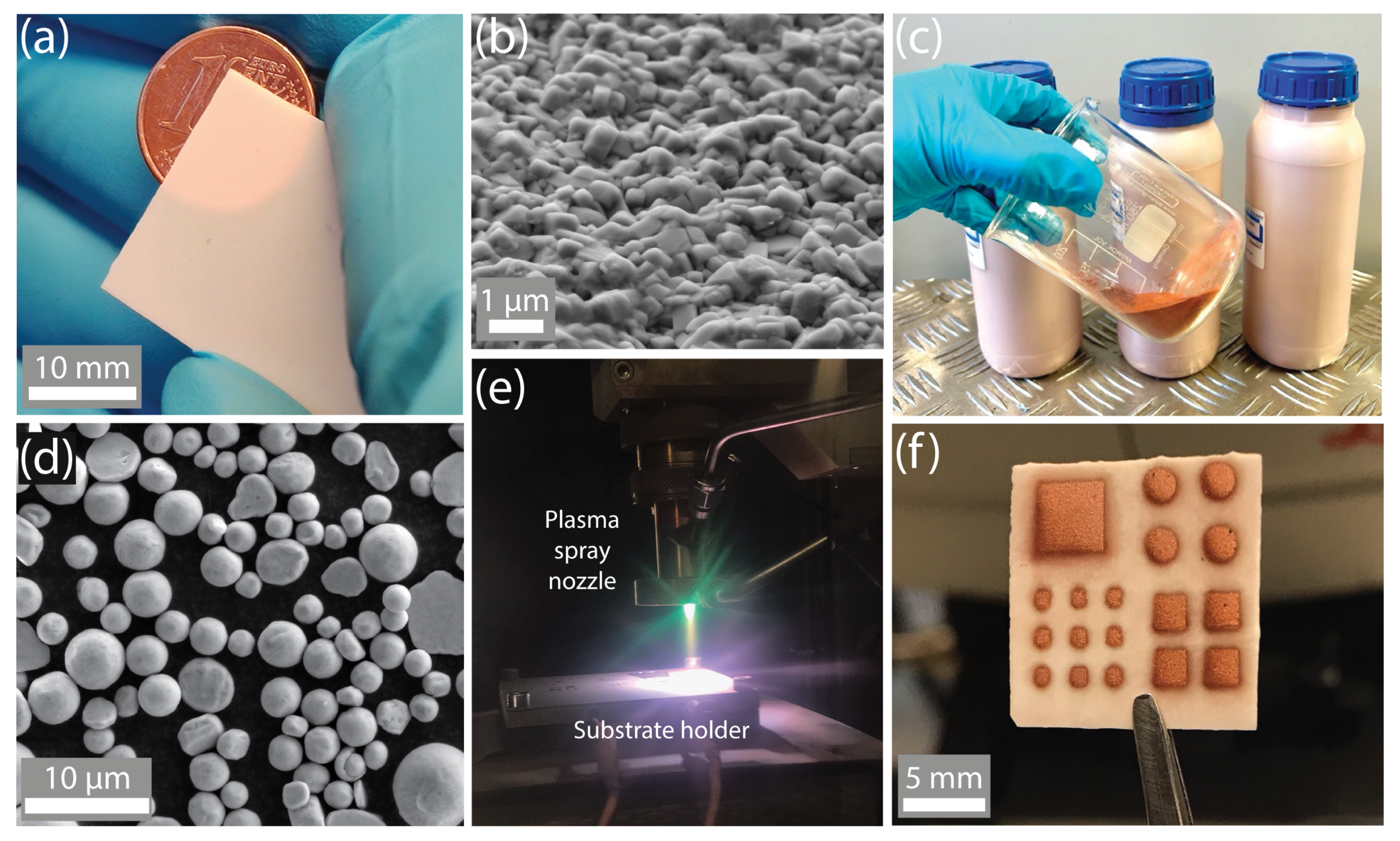
300 µm thick Li1.5Al0.5Ge1.5O12 (LAGP) substrates were obtained from MSE Supplies LLC, Tucson, AZ, USA, and used to investigate the suitability of the atmospheric plasma spraying process for comparatively thin ceramic solid electrolytes. Planar, Z r O 2 -toughened sodium beta-alumina solid-state electrolyte (BASE) with a thickness of around 1.4 mm was produced by Fraunhofer IKTS (Hermsdorf, Germany). This material is fabricated via a solid-state reaction as described elsewhere [19]. BASE was selected for sodium plating experiments with subsequent analytical investigation, as sodium metal provides strong elemental contrast in standard SEM/EDS analysis, allowing straightforward identification of plated metal layers in contrast to metallic lithium. Before the APS coating steps, the samples were cleaned with P2000 SiC sandpaper (3M, St. Paul, MN, USA). Figure 1 provides an overview of the atmospheric plasma spraying process used in this study, including substrate preparation, copper feedstock powder, and the coating procedure.

2.2. Mounting

For the atmospheric plasma spraying process, the substrates were mounted on a 5 mm thick aluminium base-plate in milled cavities with a depth of the substrate thickness plus an additional 20 µm. The sample holder with several substrates was covered by a 0.5 mm thick steel plate acting as a mask. Different shapes were cut in the mask with a pico-second laser (Cepheus Workstation, Photon Energy GmbH, Ottensoos, Germany). A multi-axis stage moves the samples underneath the plasma spray coater nozzle.

2.3. APS Coating Process

Thin copper layers were applied to various ceramic substrates using the plasma spray technique (for parameter details, see [20,21,22,23]). The used plasma gas was a mixture of argon and 0.25% hydrogen to reduce copper oxidation. An electrical discharge ignited the plasma torch at roughly 9 kV. The dissociated and partly ionized gas flame was stabilized by a high current (170 A) and comparatively low voltage (20 V). Depending on the chosen parameters, the gas flow rates varied between 15 and 30 L/min. Spherical copper powder particles with a diameter <10 µm were injected from two sides into the plasma torch, with a nitrogen-hydrogen gas mixture used as a shielding gas to focus the particle beam. The copper coating on the substrate was formed by several particles stacked upon each other. The particles were, depending on their diameter, partially or completely molten and accelerated. The two-dimensional coating was realized by moving the substrate at 255 mm/s under the stationary plasma gun. The thermal spray process was carried out in a standard atmosphere at room temperature. After the deposition, the copper-coated area was within a 5% margin of the mask feature size. After the copper coating process, all materials were transferred to a glovebox environment (Argon) and handled under inert gas or vacuum conditions from then onward. Gökçen et al. [24] demonstrated that, over a wide range of atmospheric plasma spray process parameters, an electrical conductivity of the deposited copper layers exceeding 10 MS/cm can be reproducibly achieved.

2.4. Plating Process

A battery-grade quality sodium metal chip (AOT Battery Equipment, Xiamen, China) was used as the counter-electrode, specifically for the sodium plating experiments. The sodium chip had a thickness of about 450 µm on a 30 µm thick aluminum foil carrier with a diameter of 16 mm. The overlapping area between the circular sodium chip and the rectangular BASE substrate was ~1.6 cm2. For the sodium plating tests, a 1.4 ± 0.2 mm thick BASE substrate was chosen to avoid possible damaging of the substrate during coating or from the application of the sodium counter-electrode. A pressure of about 1.25 MPa was applied for 2 min, resulting in strong adhesion of the sodium to the substrate. The counter-electrode was put on a steel plate which was connected to the positive pole of the galvanostat. The copper layer was connected to the negative pole by a prober with high surface contact to distribute the electric current and weight of the prober on the whole surface of the copper patch and avoid the risk of punching through it. The prober applied a force of F 0.6 N on the copper patch. Depending on the pad geometry, i.e., a square pad with an area of 4 mm2 or a circular pad with a radius of 1 mm (area 3.14 mm2), this corresponds to an effective contact pressure in the range of 0.15–0.19 MPa during plating, assuming ideally rigid copper patches. Compared with other experiments, this was a relatively low pressure applied during plating [25,26,27]. A Zennium potentiostat (Zahner-Elektrik GmbH & Co. KG, Kronach, Germany) with Thales XT software (5.93) was used as a galvanostat to apply a current of 2 µA on a 4 mm2 copper patch for sodium plating at the Cu|BASE interface. This corresponds to a specific current density of 0.05 mA/cm2. In the first 5 h of plating, a constant overpotential of 15 mV was observed, which increased to 184 mV after 24 h (end of plating). The height of the transferred sodium layer, assuming dense sodium metal, is given by the following equation [28]:
h P = M z · ρ · F · j · dt
Here, F = 96,453 C/mol is the Faraday constant, M = 23 g/mol is the molar mass of sodium, z = 1 is the valency, ρ = 0.971 g/cm3 is the density of sodium metal, and j · dt = 1.2 mAh/cm2, where j and t are the current density and the plating time, respectively. According to Equation (1), a plating thickness of 8.87 µm per mAh/cm2 was expected. In the experiment, 1.2 mAh/cm2 was plated at the Cu|BASE interface, which corresponded to a plating thickness of 10.64 µm. Sodium is easily detectable via standard EDS techniques; hence, no windowless system or TOF-SIMS was required.
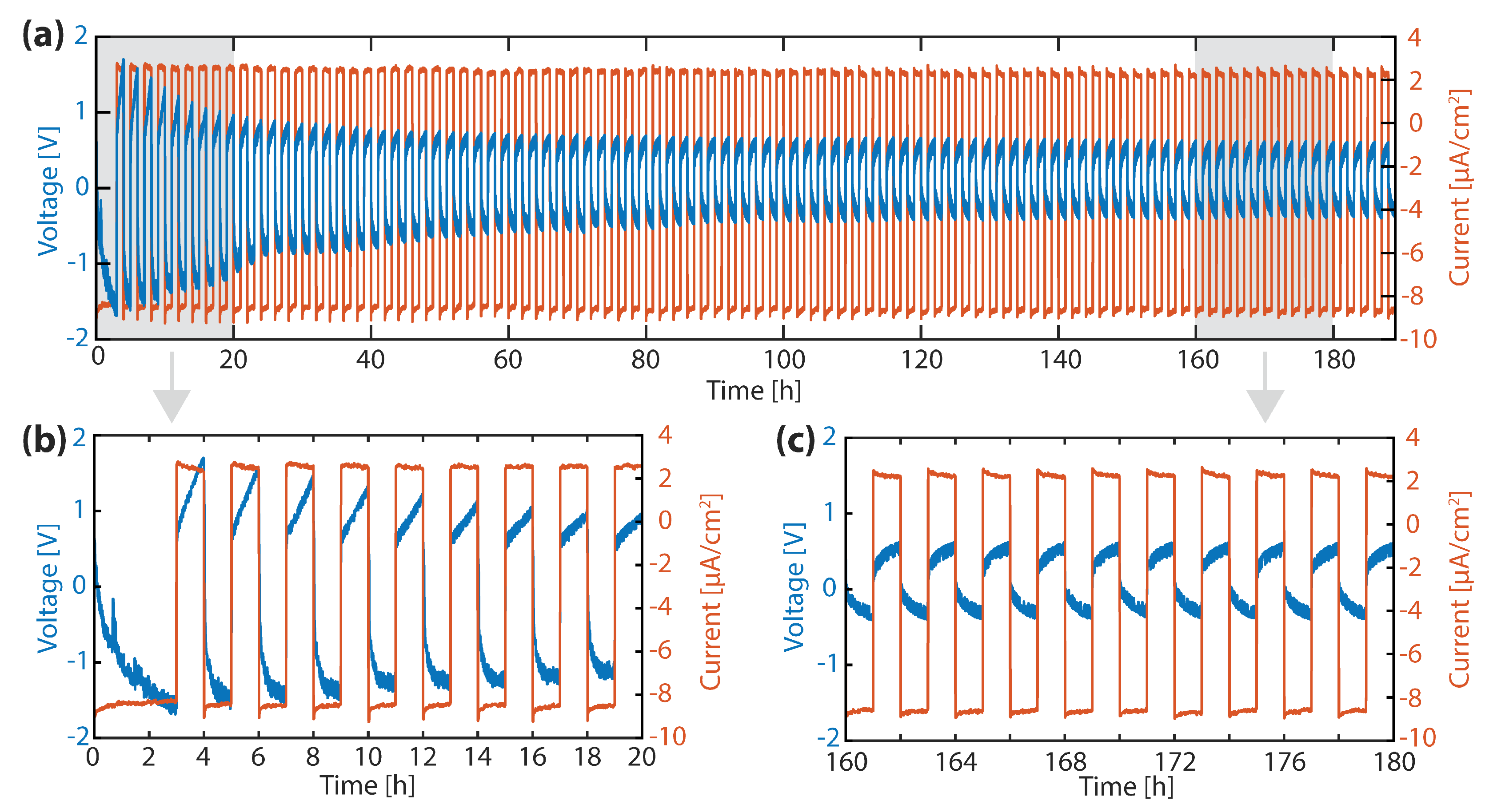
In addition to the sodium plating experiments, galvanostatic lithium plating/stripping measurements were carried out on plasma-sprayed copper current collectors deposited on LAGP substrates. The experiments were performed in a two-electrode configuration. To prepare the lithium counter electrode, metallic lithium (99.9%, Sigma-Aldrich, Merck KGaA, Darmstadt, Germany) was melted on a steel plate placed on a hot plate, after which the LAGP pellet was pressed into the molten lithium to establish a lithium reservoir at the counter electrode side. A constant current density of approximately 8.7 µA/cm2 per half-cycle was applied for lithium plating on the copper side, while a current density of approximately 2.5 µA/cm2 per half-cycle was used for stripping. The initial plating step was conducted for 3 h , whereas all subsequent half-cycles were limited to 1 h . Cycling was performed using a BTS4000 cycler (Neware Technology Limited, Shenzhen, China).

2.5. Characterization

The FIB trenches shown in Figure 2 and Figure 3 were milled using a CrossBeam 550 (Carl Zeiss AG, Oberkochen, Germany) or an Amber X (TESCAN Group, Brno, Czech Republic) equipped with a gallium ion source or xenon ion source, respectively. Samples were transferred between the glovebox and the SEMs under inert gas or vacuum conditions in dedicated shuttle systems to avoid oxidation and contamination. The beam currents were 65 nA (gallium) and 500 nA (xenon) for rough milling and low nA for subsequent polishing. Imaging was performed on a Zeiss CrossBeam 550 in low-kV mode. EDS imaging (see Figure 4a) and the linescan in Figure 2b were performed using an Ultim Max 170 (Oxford Instruments, Abingdon, UK) with 10 kV and 5 kV acceleration voltages, respectively.

3. Results

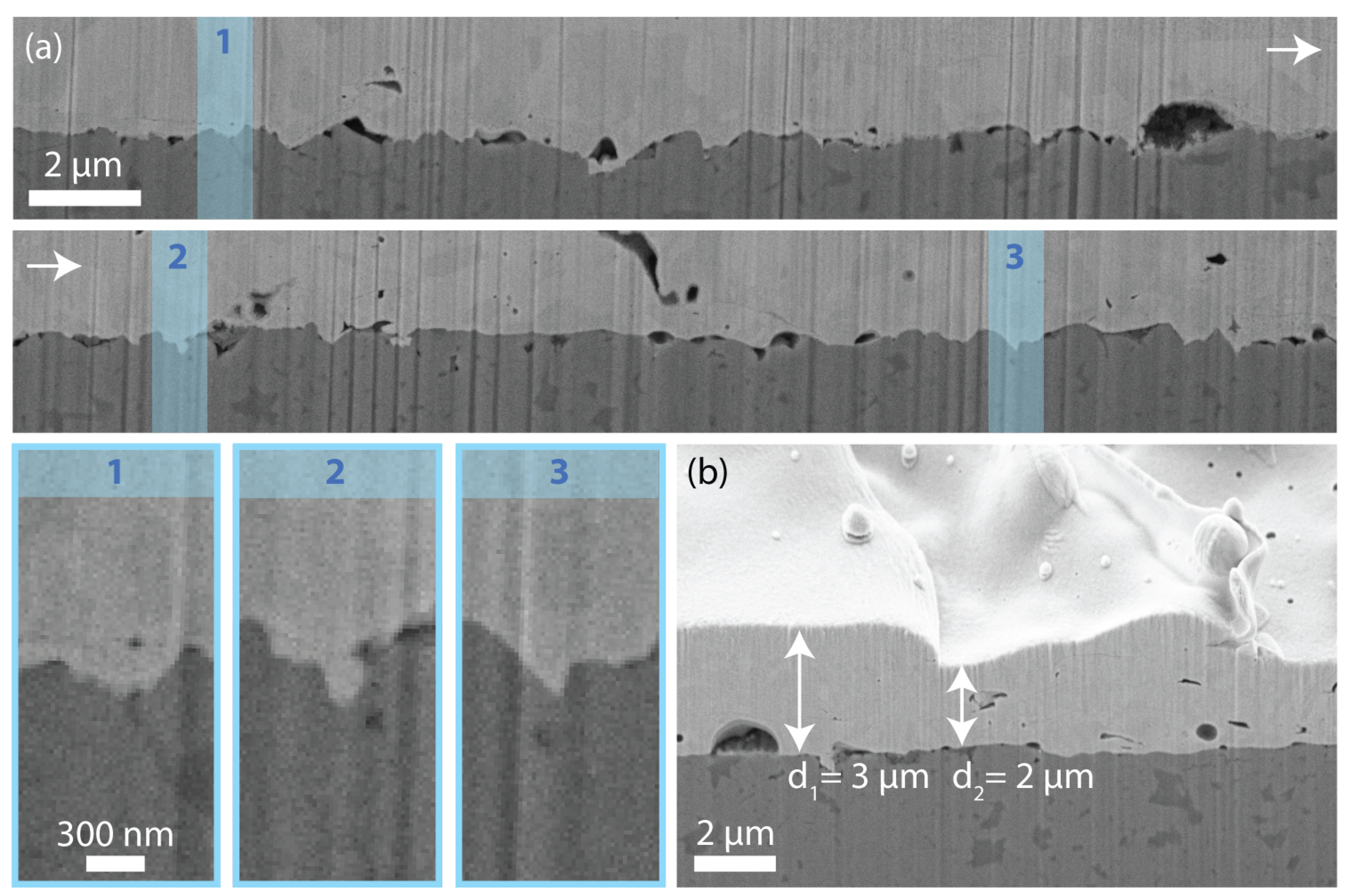
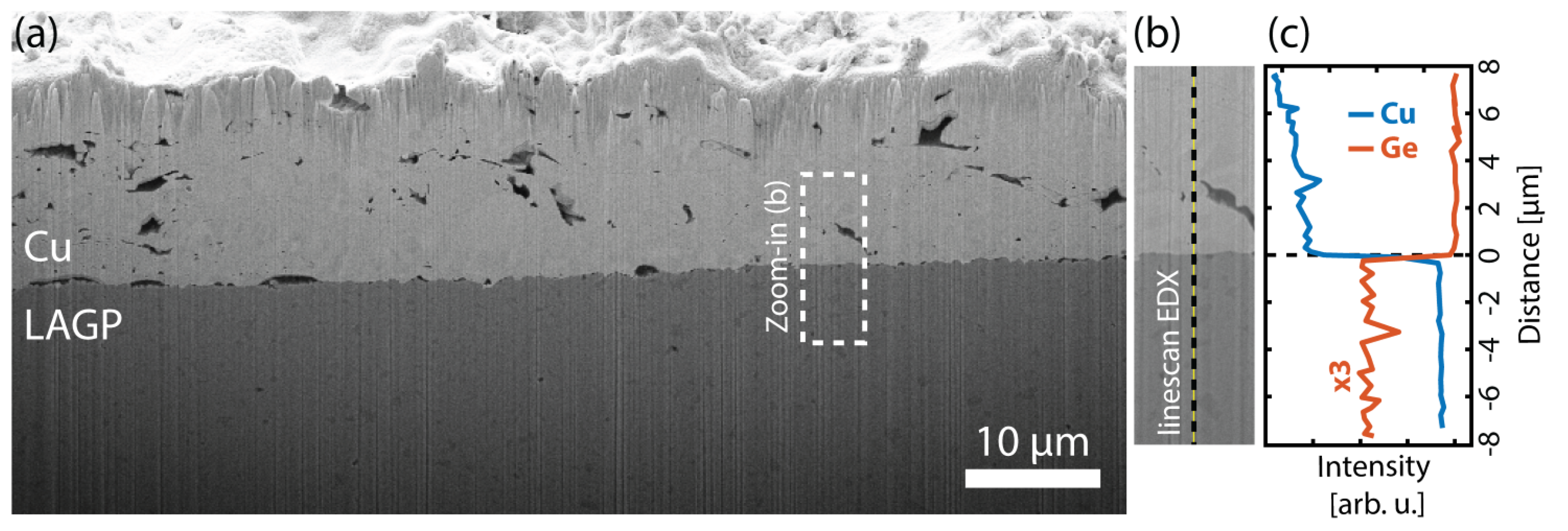
After the plasma spray deposition no obvious damage (breaking, cracks, delamination) to any sample could be identified, despite the smallest sample thickness being only 300 µm. Good adhesion between copper layer and the ceramic substrates LAGP and BASE is observed. Figure 2a shows a FIB cross section through copper on LAGP substrate. The copper layer appears homogeneous and dense with some minor closed pores and granular copper structures on the surface. To investigate the interface Cu|LAGP for potential chemical reactions, corrosion or mixing of elements of the substrate from and into copper, an EDS line scan was performed (Figure 2b,c). Here, the copper and germanium signals are used representatively to investigate the transition. Only two phases are visible, no additional interphase was observed. The EDS signals of germanium and copper in the line scan in Figure 2c show a sharp transition within less than 0.5 µm. The interaction zone of the EDS signal regions was simulated in CASINO to be smaller than 50 nm, which is much smaller compared to the observed signal change. Figure 3a shows the interface quality and interlocking nature of the deposition in greater detail. Small geometries and cavities are filled with the sprayed copper, even in the sub-µm to 100 nm range (see highlighted areas in (a) and corresponding magnified panels 1, 2, 3). This justifies the assumption that the actual contact area achievable with the plasma spraying process is of the same order of magnitude as the geometric contact area, or perhaps even greater [29]. While the microstructure of the copper layer in some regions in Figure 2 and Figure 3 appears similar to cast or rolled copper [30], in other regions it appears as stacked and cold-formed compacted copper particles. Channeling contrast is visible in Figure 3 which indicates the formation of a polycrystalline microstructure independent of former particles sizes and structures. Figure 3b shows the achieved minimum thickness of a plasma sprayed copper CC of around 2–3 µm. In this section of the sample the sprayed copper shows a smooth surface structure with a variation of ± 0.5 µm.
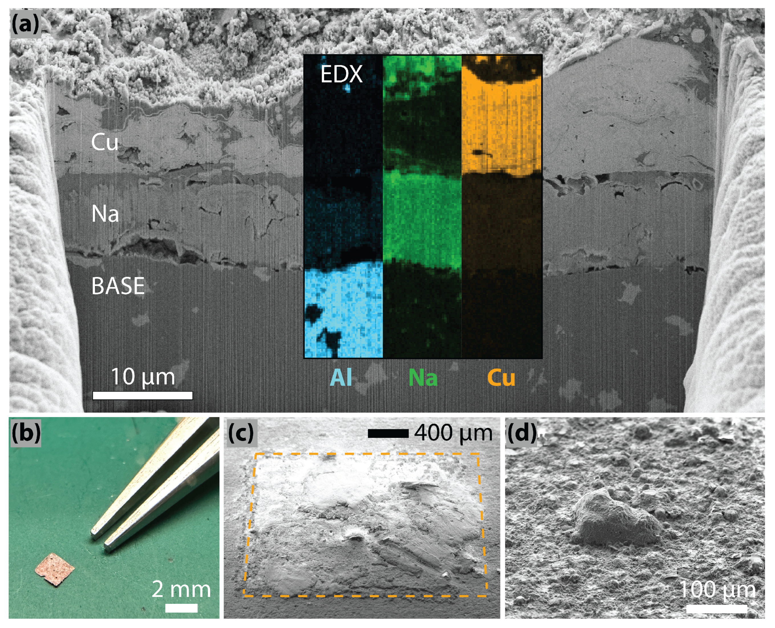
A plating test as described in Section 2.4 was performed to demonstrate the suitability of the plasma spray deposition for the fabrication of a form-fitting current collector on solid electrolyte, which is of fundamental importance for high-quality initial cycling in reservoir-free solid-state batteries. Figure 4 shows a cross section through plated sodium metal along the Cu|BASE interface. A homogeneous layer of metallic sodium with minor cavities was successfully formed (a). Within the FIB trench the sodium layer is uniformly plated and about 10 µm thick in accordance with Equation (1). Sodium can be found in pores within the copper layer and on its surface.
The copper layer was peeled off the plated sodium layer as one single intact piece with tweezers (Figure 4b). Figure 4c shows the plating area after the removal of the copper patch. Sodium was plated almost everywhere between the copper and the BASE substrate, even though some topography variation can be observed. The structure in the lower right part of Figure 4c can be attributed to the harsh removal of the copper layer by tweezers. Figure 4d shows metallic sodium which had emerged from a FIB trench site within 24 h after initial milling. Figure 5 shows the voltage profile over 93 plating/stripping cycles. Stable cycling behavior with a consistent overpotential throughout the experiment was observed, indicating a robust and stable interface between the plasma-sprayed copper current collector and the solid electrolyte. No signs of short-circuiting or rapid degradation were detected over the entire cycling period.

4. Discussion

In this paper, we demonstrated the successful fabrication of a copper current collector for anode-free solid-state batteries via atmospheric plasma spraying and the successful plating of a sodium metal layer at the so produced Cu|BASE interface. It shows that essential properties of such an interface for use in reservoir-free solid-state batteries are met. These include a homogeneous coating of the layer itself, its stability against side reactions at elevated coating temperatures and plating conditions, such as internal plating stress. A homogeneous sodium layer was plated with a thickness consistent with the transferred charge and in the correct order of magnitude for application in a solid-state battery. The plating was successful almost everywhere underneath the sprayed CC.
The observation of two distinct grayscale contrast regions in Figure 2, corresponding to the copper coating and the solid electrolyte substrate, indicates that no visible interface phases are formed during APS. Despite the elevated temperature of the molten copper particles upon impact, neither pronounced chemical reactions nor interdiffusion leading to detectable alloy formation appear to occur at the interface. This suggests that the process preserves the chemical integrity of both materials under the applied deposition conditions. The copper layer thicknesses obtained in this study (Figure 2 and Figure 3) demonstrate that APS can be employed to fabricate not only comparatively thick current collectors (8–12 µm), which are typical for state-of-the-art copper coatings [31,32,33], but also substantially thinner layers in the range of 2–3 µm. This capability is particularly relevant given the high density of copper (8.96 g/cm3 [12]) and its increasing demand in other energy-related applications. Reducing the thickness of the anode current collector therefore represents an effective strategy to lower cell mass and improve specific energy. While previous work has shown that ultra-thin copper layers down to 500 nm can significantly enhance specific energy when deposited by magnetron sputtering [34], the mechanical stability of micrometer-scale copper layers under repeated lithium or sodium plating and stripping in reservoir-free configurations remains an open question.
Although the solid electrolyte thickness used in this work (300 µm) exceeds the target range for practical cell designs, the present results provide valuable insight into the suitability of APS for forming current collectors on rough ceramic surfaces and should be transferable to thinner SEs. For competitive solid-state battery designs, separator thicknesses in the range of approximately 20–30 µm are generally considered necessary to achieve gravimetric and volumetric energy densities comparable to conventional lithium-ion cells [12,35,36]. While the present study does not yet address this target thickness regime, the demonstrated compatibility of atmospheric plasma spraying with mechanically fragile ceramic substrates represents an essential processing prerequisite for future investigations on substantially thinner solid electrolytes.
In contrast to vacuum-based techniques or approaches relying on complex interlayers, APS enables rapid deposition without additional chemical processing steps or auxiliary materials. The conformal adhesion of the copper layer to the unpolished solid electrolyte surface suggests that this technique is well suited to accommodate surface roughness, which is often unavoidable in ceramic electrolytes. The sodium metal plating experiment further highlights the interface quality of the plasma sprayed copper current collector. It is important to note that the sodium plating experiments in this study were performed under comparatively low external pressure during cycling (approximately 0.15–0.19 MPa), which is substantially lower than the pressures commonly applied in the literature to achieve stable sodium or lithium metal cycling at solid electrolyte interfaces [25,26,27]. In these previous works, elevated pressures are typically maintained over many plating/stripping cycles to preserve interfacial contact and suppress chemo-mechanical degradation.
In the present work, the applied pressure is sufficient to enable homogeneous initial sodium plating at the Cu|SE interface but does not yet address long-term cycling stability. It is therefore expected that higher pressures may again become necessary during repeated plating and stripping to accommodate morphological evolution, stress accumulation, and potential interfacial degradation of the metal anode. Nevertheless, the ability to achieve uniform and dense initial sodium deposition under such reduced pressure represents a relevant result. It indicates that the form-fitting and mechanically interlocked plasma-sprayed copper current collector effectively minimizes current constriction effects during the formation step, thereby lowering the pressure required to establish high-quality interfacial contact at the beginning of cell operation. The intimate contact between copper and solid electrolyte likely increases the effective interface area beyond the idealized geometric interface, thereby reducing local current densities. This effect may contribute to the homogeneous growth of a dense sodium layer observed under comparatively low external pressure. The measured sodium layer thickness is consistent with the value predicted by Equation (1) and exhibits a planar morphology across the copper-coated area (Figure 4), indicating uniform electrochemical activity.
The observation of sodium creep emerging from a focused-ion-beam trench after prolonged plating (Figure 4b) suggests the presence of internal stresses within the deposited sodium layer. Such stresses may assist in filling interface voids at the Na|SE boundary during initial plating. However, whether nano-scale mechanical interlocking at the copper–electrolyte interface can provide sufficient adhesion to prevent delamination during extended cycling remains to be clarified. Future studies employing thinner solid electrolyte substrates and repeated plating/stripping cycles will be necessary to assess the long-term mechanical and electrochemical stability of plasma sprayed current collectors. Overall, the results indicate that APS offers a promising and comparatively simple route to fabricate current collectors with well-defined thickness, good interface contact, and low processing complexity. Compared to sputtering, thermal evaporation, or electron-beam deposition, the technique combines rapid processing with scalable material handling while achieving comparable interface quality. These characteristics make APS a compelling candidate for further investigation in the context of anode-free solid-state batteries, such as porous ceramic scaffold architectures [12,28,37,38] or in combination with other spraying techniques in battery manufacturing [39,40,41].

Author Contributions

Conceptualization, A.B. and T.P.; methodology, A.B., T.P. and M.O.; software, F.V.; formal analysis, A.B., T.P., F.V. and B.U.; investigation, A.B., T.P., M.O., F.V. and B.U.; resources, M.O., C.D., M.M. and G.S.; writing—original draft, A.B. and T.P.; writing—review & editing, A.B., T.P., F.V., C.D. and B.U.; visualization, A.B. and T.P.; supervision, J.F. and S.C.; project administration, J.F. and S.C.; funding acquisition, A.B., J.F. and S.C. All authors have read and agreed to the published version of the manuscript.

Funding

This work was funded by the German Federal Ministry of Education and Research (BMBF, now Federal Ministry of Research, Technology and Space—BMFTR) under grant numbers 3DPrintBatt 16BZF351D and CoCoBatt 01IF23676N (IGF program via AiF, supported by the Research Association 3D-MID), and by the German Federal Ministry for Economic Affairs and Climate Action (BMWK, now Federal Ministry for Economic Affairs and Energy (BMWE)) under grant number NaNiBatt 03XP0520A.

Data Availability Statement

The original contributions presented in this study are included in the article. Further inquiries can be directed to the corresponding author.

Conflicts of Interest

Florian Vollnhals was employed at the Institut für Nanotechnologie und korrelative Mikroskopie gGmbH (INAM) during the experiments, a publicly funded non-profit research organization. Martin Muckelbauer was employed at FAU and is affiliated with Powerlyze GmbH, which acted as an unpaid consultant in the project “CoCoBatt” (01IF23676N). Several authors (Andre Borchers, Timo Paschen, Manuela Ockel, Martin Muckelbauer, Jörg Franke, and Silke Christiansen) are co-inventors on patent applications DE 10 2022 209 709 A1 and WO 2024/056299 A1. The authors declare that these affiliations, consulting activities, and patent applications did not influence the scientific integrity or objectivity of this work. All other authors declare no conflicts of interest.

References

  1. Krauskopf, T.; Hartmann, H.; Zeier, W.G.; Janek, J. Toward a Fundamental Understanding of the Lithium Metal Anode in Solid-State Batteries—An Electrochemo-Mechanical Study on the Garnet-Type Solid Electrolyte Li6.25Al0.25La3Zr2O12. ACS Appl. Mater. Interfaces 2019, 11, 14463–14477. [Google Scholar] [CrossRef]
  2. Balaish, M.; Kim, K.J.; Chu, H.; Zhu, Y.; Gonzalez-Rosillo, J.C.; Kong, L.; Paik, H.; Weinmann, S.; Hood, Z.D.; Hinricher, J.; et al. Emerging processing guidelines for solid electrolytes in the era of oxide-based solid-state batteries. Chem. Soc. Rev. 2025, 54, 8925–9007. [Google Scholar] [CrossRef] [PubMed]
  3. Chang, C.Y.; Wang, C.C.; Cheng, C.H.; Lu, Y.L.; Lin, S.H.; Granwehr, J.; Windmüller, A.; Tsai, C.L.; Eichel, R.A.; Chiu, K.F. Enhanced stability and high rate capability of garnet solid-state electrolyte interface through integration of nanoscale Li4Ti5O12 for Li battery applications. J. Power Sources 2025, 652, 237593. [Google Scholar] [CrossRef]
  4. Melvin, D.L.; Siniscalchi, M.; Spencer-Jolly, D.; Hu, B.; Ning, Z.; Zhang, S.; Bu, J.; Marathe, S.; Bonnin, A.; Ihli, J.; et al. High plating currents without dendrites at the interface between a lithium anode and solid electrolyte. Nat. Energy 2025, 10, 1205–1214. [Google Scholar] [CrossRef]
  5. Eckhardt, J.K.; Kremer, S.; Fuchs, T.; Minnmann, P.; Schubert, J.; Burkhardt, S.; Elm, M.T.; Klar, P.J.; Heiliger, C.; Janek, J. Influence of Microstructure on the Material Properties of LLZO Ceramics Derived by Impedance Spectroscopy and Brick Layer Model Analysis. ACS Appl. Mater. Interfaces 2023, 15, 47260–47277. [Google Scholar] [CrossRef]
  6. Eckhardt, J.K.; Fuchs, T.; Burkhardt, S.; Klar, P.J.; Janek, J.; Heiliger, C. Guidelines for Impedance Analysis of Parent Metal Anodes in Solid-State Batteries and the Role of Current Constriction at Interface Voids, Heterogeneities, and SEI. Adv. Mater. Interfaces 2023, 10, 2202354. [Google Scholar] [CrossRef]
  7. Alexander, G.V.; Shi, C.; O’Neill, J.; Wachsman, E.D. Extreme lithium-metal cycling enabled by a mixed ion- and electron-conducting garnet three-dimensional architecture. Nat. Mater. 2023, 22, 1136–1143. [Google Scholar] [CrossRef]
  8. Krauskopf, T.; Dippel, R.; Hartmann, H.; Peppler, K.; Mogwitz, B.; Richter, F.H.; Zeier, W.G.; Janek, J. Lithium-Metal Growth Kinetics on LLZO Garnet-Type Solid Electrolytes. Joule 2019, 3, 2030–2049. [Google Scholar] [CrossRef]
  9. Zhang, X.; Wang, Q.J.; Harrison, K.L.; Roberts, S.A.; Harris, S.J. Pressure-Driven Interface Evolution in Solid-State Lithium Metal Batteries. Cell Rep. Phys. Sci. 2020, 1, 100012. [Google Scholar] [CrossRef]
  10. Han, X.; Gong, Y.; Fu, K.; He, X.; Hitz, G.T.; Dai, J.; Pearse, A.; Liu, B.; Wang, H.; Rubloff, G.; et al. Negating interfacial impedance in garnet-based solid-state Li metal batteries. Nat. Mater. 2017, 16, 572–579. [Google Scholar] [CrossRef]
  11. Ruan, Y.; Lu, Y.; Li, Y.; Zheng, C.; Su, J.; Jin, J.; Xiu, T.; Song, Z.; Badding, M.E.; Wen, Z. A 3D Cross-Linking Lithiophilic and Electronically Insulating Interfacial Engineering for Garnet-Type Solid-State Lithium Batteries. Adv. Funct. Mater. 2021, 31, 2007815. [Google Scholar] [CrossRef]
  12. Kriegler, J.; Finsterbusch, M.; Liang, Y.; Jaimez-Farnham, E.; Zaeh, M.F. A perspective on the design, manufacturing, and energy content of oxide all-solid-state batteries with scaffold-based composite cathodes. J. Power Sources 2024, 596, 234091. [Google Scholar] [CrossRef]
  13. Lu, Y.; Zhao, C.Z.; Yuan, H.; Cheng, X.B.; Huang, J.Q.; Zhang, Q. Critical Current Density in Solid-State Lithium Metal Batteries: Mechanism, Influences, and Strategies. Adv. Funct. Mater. 2021, 31, 2009925. [Google Scholar] [CrossRef]
  14. Liu, Y.; Sun, Q.; Zhao, Y.; Wang, B.; Kaghazchi, P.; Adair, K.R.; Li, R.; Zhang, C.; Liu, J.; Kuo, L.Y.; et al. Stabilizing the Interface of NASICON Solid Electrolyte against Li Metal with Atomic Layer Deposition. ACS Appl. Mater. Interfaces 2018, 10, 31240–31248. [Google Scholar] [CrossRef]
  15. Ortmann, T.; Fuchs, T.; Eckhardt, J.K.; Ding, Z.; Ma, Q.; Tietz, F.; Kübel, C.; Rohnke, M.; Janek, J. Deposition of Sodium Metal at the Copper-NaSICON Interface for Reservoir-Free Solid-State Sodium Batteries. Adv. Energy Mater. 2024, 14, 2302729. [Google Scholar] [CrossRef]
  16. Tseng, K.T.; Lee, K.; Sakamoto, J. Enabling “Sodium-Metal-Free” Manufacturing of Solid-State Batteries. ACS Energy Lett. 2024, 9, 4544–4549. [Google Scholar] [CrossRef]
  17. Lowack, A.; Grun, P.; Anton, R.; Auer, H.; Nikolowski, K.; Partsch, M.; Kusnezoff, M.; Michaelis, A. Sputtered Zero-Excess Electrodes with Metallic Seed Layers for Solid-State Sodium Batteries. Batter. Supercaps 2025, 8, e202400364. [Google Scholar] [CrossRef]
  18. Fertig, M.P.; Skadell, K.; Schulz, M.; Dirksen, C.; Adelhelm, P.; Stelter, M. From High- to Low-Temperature: The Revival of Sodium-Beta Alumina for Sodium Solid-State Batteries. Batter. Supercaps 2022, 5, e202100131. [Google Scholar] [CrossRef]
  19. Dirksen, C.L.; Skadell, K.; Schulz, M.; Fertig, M.P.; Stelter, M. Influence of 3d transition metal doping on lithium stabilized na-β″-alumina solid electrolytes. Materials 2021, 14, 5389. [Google Scholar] [CrossRef]
  20. Hensel, A.; Schwarzer, C.; Scheetz, M.; Kaloudis, M.; Franke, J. Investigations of silver sintered interconnections 3-dimensional ceramics with plasma based additive copper metallizations. In Proceedings of the 2018 IEEE 20th Electronics Packaging Technology Conference, Singapore, 4–7 December 2018; pp. 416–421. [Google Scholar] [CrossRef]
  21. Ockel, M.; Borchers, A.; Frohlich, J.; Petersen, M.; Paschen, T.; Christiansen, S.; Franke, J. Atmospheric Plasma Spraying for Copper Coating of Ceramic Solid Electrolytes for Anode-Free Solid-State Batteries with Increased Interfacial Contact. In Proceedings of the 2024 1st International Conference on Production Technologies and Systems for E-Mobility, Bamberg, Germany, 5–6 June 2024. [Google Scholar] [CrossRef]
  22. Stoltenhoff, T.; Borchers, C.; Gärtner, F.; Kreye, H. Microstructures and key properties of cold-sprayed and thermally sprayed copper coatings. Surf. Coat. Technol. 2006, 200, 4947–4960. [Google Scholar] [CrossRef]
  23. Schwarzer, C.; Hensel, A.; Roth, F.; Franke, J.; Kaloudis, M. Investigation of Pressureless Sintered Interconnections on Plasma Based Additive Copper Metallization. In Proceedings of the 2020 IEEE 70th Electronic Components and Technology Conference, Orlando, FL, USA, June 2020; pp. 1592–1600. [Google Scholar] [CrossRef]
  24. Gökçen, A.; Ockel, M.; Petersen, M.; Thielen, N.; Franke, J.; Risch, F. Optimizing Thin Electric Functional Copper Coatings via Atmospheric Plasma Spray. In Proceedings of the International Thermal Spray Conference, Vancouver, BC, Canada, 5–8 May 2025; pp. 192–197. [Google Scholar] [CrossRef]
  25. Jiao, W.; Zohair, M.; Eaves-Rathert, J.; Ramamurthy, J.; Harkaway, A.; Mort, R.; Wheaton, J.; Jiang, S.; Martin, S.W.; Pint, C.L. Critical Role of Pressure for Chemo-Mechanical-Induced Stability of Sodium Metal Battery Anodes. ACS Energy Lett. 2023, 8, 2711–2717. [Google Scholar] [CrossRef]
  26. Singh, V.K.; Schuler, J.; Ortmann, T.; Ziegler, M.; Janek, J.; Nazar, L.F. High Coulombic Efficiency Plating and Stripping of Sodium for Reservoir-Free Solid-State Batteries at Low Stack Pressure. ACS Energy Lett. 2025, 10, 3663–3669. [Google Scholar] [CrossRef]
  27. Fuchs, T.; Ortmann, T.; Becker, J.; Haslam, C.G.; Ziegler, M.; Singh, V.K.; Rohnke, M.; Mogwitz, B.; Peppler, K.; Nazar, L.F.; et al. Imaging the microstructure of lithium and sodium metal in anode-free solid-state batteries using electron backscatter diffraction. Nat. Mater. 2024, 23, 1678–1685. [Google Scholar] [CrossRef] [PubMed]
  28. Lohrberg, O.; Maletti, S.; Heubner, C.; Schneider, M.; Michaelis, A. Understanding Li Plating and Stripping Behavior in Zero-Excess Li Metal Batteries Using Operando Dilatometry. J. Electrochem. Soc. 2022, 169, 030543. [Google Scholar] [CrossRef]
  29. Zhang, S.; Hu, B.; Geng, Z.; Gao, X.; Spencer-Jolly, D.; Melvin, D.L.; Ning, Z.; Li, G.; Jenkins, M.; Wang, L.; et al. Influence of contouring the lithium metal/solid electrolyte interface on the critical current for dendrites. Energy Environ. Sci. 2024, 17, 1448–1456. [Google Scholar] [CrossRef]
  30. Okayasu, M.; Muranaga, T.; Endo, A. Analysis of microstructural effects on mechanical properties of copper alloys. J. Sci. Adv. Mater. Devices 2017, 2, 128–139. [Google Scholar] [CrossRef]
  31. Zhou, J.; Qin, J.; Zhan, H. Copper Current Collector: The Cornerstones of Practical Lithium Metal and Anode–Free Batteries. ChemPhysChem 2024, 25, e202400007. [Google Scholar] [CrossRef]
  32. Yang, L.; Weng, W.; Zhu, H.; Chi, X.; Tan, W.; Wang, Z.; Zhong, S. Preparing ultra-thin copper foil as current collector for improving the LIBs performances with reduced carbon footprint. Mater. Today Commun. 2023, 35, 105952. [Google Scholar] [CrossRef]
  33. Liu, J.; Jia, H.; Nguyen, D.; Liu, J.; Fang, C. Fabricating ultralight and ultrathin copper current collectors for high-energy batteries. eScience 2024, 4, 100271. [Google Scholar] [CrossRef]
  34. Ye, Y.; Chou, L.Y.; Liu, Y.; Wang, H.; Lee, H.K.; Huang, W.; Wan, J.; Liu, K.; Zhou, G.; Yang, Y.; et al. Ultralight and fire-extinguishing current collectors for high-energy and high-safety lithium-ion batteries. Nat. Energy 2020, 5, 786–793. [Google Scholar] [CrossRef]
  35. Wu, J.; Yuan, L.; Zhang, W.; Li, Z.; Xie, X.; Huang, Y. Reducing the thickness of solid-state electrolyte membranes for high-energy lithium batteries. Energy Environ. Sci. 2021, 14, 12–36. [Google Scholar] [CrossRef]
  36. Yim, C.H.; Houache, M.S.; Baranova, E.A.; Abu-Lebdeh, Y. Understanding key limiting factors for the development of all-solid-state-batteries. Chem. Eng. J. Adv. 2023, 13, 100436. [Google Scholar] [CrossRef]
  37. Jaschin, P.W.; Tang, C.R.; Wachsman, E.D. High-rate cycling in 3D dual-doped NASICON architectures toward room-temperature sodium-metal-anode solid-state batteries. Energy Environ. Sci. 2024, 17, 727–737. [Google Scholar] [CrossRef]
  38. Jaschin, P.W.; Tang, C.R.; Wachsman, E.D. Fast Charging and Low Temperature Capabilities of Sodium Solid-State Batteries Enabled by Thin NASICON Bilayer Architecture. ACS Energy Lett. 2025, 10, 2610–2616. [Google Scholar] [CrossRef]
  39. Doerrer, C.; Metzler, M.; Matthews, G.; Bu, J.; Spencer-Jolly, D.; Bruce, P.G.; Pasta, M.; Grant, P.S. Spraying Li6PS5Cl and silver-carbon multilayers to facilitate large-scale fabrication of all-solid-state batteries. Device 2024, 2, 100468. [Google Scholar] [CrossRef]
  40. Hennerici, L.; Ficht, P.; Schamel, M.; Mansfeld, U.; Linz, M.; Paulus, D.; Kita, J.; Danzer, M.A.; Moos, R. Lithium All-Solid-State Batteries Fabricated at Room Temperature by the Powder Aerosol Deposition Method with Garnet-Type Electrolyte and Graded Composite Cathode. Adv. Mater. Technol. 2025, 10, 2400745. [Google Scholar] [CrossRef]
  41. Bu, X.C.; Chen, N.; Luo, X.T.; Li, C.J. Plasma Spray Deposition of Na3Zr2Si2PO12 Electrolyte for High-Performance All-Solid-State Sodium-Ion Battery. J. Therm. Spray Technol. 2025, 34, 495–505. [Google Scholar] [CrossRef]
Figure 1. The plasma spray coating process for LAGP: (a) 300 µm thin LAGP substrate; (b) SEM image of the rough surface of the ceramic substrate; (c) raw copper powder for atmospheric plasma spraying; (d) SEM image of the microstructure and size distribution of the raw copper powder; (e) snapshot during the coating process of copper on solid electrolyte substrate; and (f) coated copper pads of various geometries and sizes on the ceramic substrate.
Batteries 12 00142 g001
Figure 2. (a) SEM micrograph of an FIB cross-section of Cu on LAGP. (b) Zoomed-in image of dashed region in (a). (c) EDS signal of Cu and Ge along the dashed line in (b). For visualization, the Ge signal was enhanced compared with that for Cu.
Batteries 12 00142 g002
Figure 3. SEM micrographs of the interface region of the coated Cu on LAGP. (a) Overview of the interlocking between the copper and substrate demonstrated along a wide interface distance. The white arrows indicate the continuation of the image. The blue highlighted regions (1, 2 and 3) are shown as zoomed sections. (b) Copper layer processed with optimized parameters for a thin coating.
Batteries 12 00142 g003
Figure 4. APS deposited Cu on the BASE sample after sodium plating along the interface. (a) SEM image with EDS inset of a cross-section after successful sodium plating. (b) Peeled-off copper layer. (c) Remaining plated sodium on the BASE surface after removing the copper coating. (d) Sodium metal growing out of the FIB trench after 24 h.
Batteries 12 00142 g004
Figure 5. Galvanostatic lithium plating/stripping at the interface Cu|LAGP. Voltage profiles (blue) and current density (red) are shown as a function of time. (a) Long-term cycling over 93 cycles. (b) Enlarged view of initial cycles. (c) Enlarged view of cycle 79 to 89, highlighting the evolution of the voltage profile.
Batteries 12 00142 g005
Disclaimer/Publisher’s Note: The statements, opinions and data contained in all publications are solely those of the individual author(s) and contributor(s) and not of MDPI and/or the editor(s). MDPI and/or the editor(s) disclaim responsibility for any injury to people or property resulting from any ideas, methods, instructions or products referred to in the content.