1. Introduction
The rapid development of artificial intelligence, edge computing, and data-intensive information processing requires computing hardware with higher bandwidth, lower latency, and reduced energy consumption. However, conventional von Neumann architectures suffer from the memory-wall bottleneck because memory and processing units are physically separated, leading to frequent data transfer and high energy dissipation. Since the memristor was theoretically proposed by Chua [
1] and experimentally demonstrated in nanoscale TiO
2-based devices by Strukov et al. [
2], memristive devices have been widely regarded as promising candidates for nonvolatile memory, in-memory computing, and neuromorphic hardware. Their two-terminal structure, scalability, nonvolatile resistance modulation, and crossbar compatibility provide important advantages for highly parallel and energy-efficient computing systems [
3,
4,
5,
6].
In particular, memristor-based artificial synapses are attractive for neuromorphic computing because their conductance states can be dynamically modulated by electrical stimuli, enabling the emulation of biological synaptic functions such as excitatory postsynaptic current, paired-pulse facilitation, short-term plasticity, and long-term memory. These characteristics make memristive synapses promising for low-power artificial neural networks, edge intelligence, adaptive sensory systems, and hardware-based brain-inspired computing. Recent studies have further extended their application prospects to flexible near-sensor intelligent systems, wearable healthcare, intelligent sensing, and neuromorphic diagnostic platforms [
7,
8]. Therefore, developing low-voltage, stable, and energy-efficient memristive synaptic devices remains highly important for future neuromorphic electronics.
In-memory and neuromorphic computing based on memristive devices has advanced rapidly in recent years. Memristor and memtransistor arrays have demonstrated broad potential in analogue signal and image processing, hardware-implemented convolutional neural networks, self-adaptive in situ learning, high-precision analogue computing, and resistive-memory-based compute-in-memory chips [
9,
10,
11,
12,
13,
14]. In addition to these computing functions, memristive devices can emulate synaptic behaviors through electrically tunable conductance states. Typical functions such as paired-pulse facilitation, short-term plasticity, long-term potentiation/depression, excitatory postsynaptic responses, and reservoir-type temporal processing have been realized in various memristive systems [
15,
16,
17,
18]. For example, phase-change memtransistive synapses have enabled mixed-plasticity neural computation, further demonstrating the value of internal state dynamics for brain-inspired hardware [
19].
Recently, magnetic-field-modulated resistive switching has attracted increasing attention because magnetic interactions provide an additional degree of freedom for regulating carrier transport, oxygen-vacancy migration, and synaptic plasticity. Magnetic-field-dependent changes in resistive-switching behavior have been reported in Ag/BiFeO
3/FTO RRAM devices and Cu/(CoFeB)
x(LiNbO
3)
100−x/LiNbO
3/Ni nanocomposite-based memristive structures [
20,
21]. More recently, Mn-doped GeSe semiconductor memristors exhibiting Curie–Weiss-type magnetic-field tuning have realized simultaneous modulation of resistive switching and artificial synaptic behaviors [
22]. In addition, Pt/TiN/ZnO/SnO
2/ZnO/Pt multilayer memristors have shown analog switching and synaptic functions for neuromorphic computing [
23].
Despite these advances, practical implementation of memristive synapses in oxide and ferrite-based memristive systems still faces several key challenges. First, many oxide-based memristors require a forming process or relatively high operating voltage, which increases energy consumption and limits their suitability for low-power neuromorphic systems. Second, the stochastic formation and rupture of conductive filaments often lead to cycle-to-cycle and device-to-device variability, degrading the reliability of resistance-state modulation and neural-network accuracy. Third, unstable defect distributions, uncontrolled interfacial reactions, and poor film crystallinity can deteriorate retention behavior, switching uniformity, and synaptic plasticity. Therefore, developing memristive devices with low operating voltage, reliable resistance modulation, controllable defect chemistry, and stable synaptic responses remains a key challenge for neuromorphic electronics [
5,
6,
24,
25,
26,
27].
Metal-oxide memristors are among the most extensively investigated systems because of their rich defect chemistry and tunable ionic/electronic transport properties. Their resistive switching behavior is generally associated with oxygen-vacancy migration, local redox reactions, conductive filament evolution, and interfacial barrier modulation [
25,
26,
27]. Recent studies have shown that regulating oxygen-vacancy concentration, cation valence states, and interface quality effectively improves switching voltage, resistance window, endurance, and synaptic characteristics [
27,
28,
29,
30,
31,
32,
33,
34,
35]. Post-deposition annealing is another effective approach for tailoring crystallinity, defect distribution, and electrode/oxide interfaces, thereby optimizing both resistive switching and artificial synaptic behavior [
29,
30,
31].
Compared with conventional binary oxides, multicomponent oxides provide a broader materials platform for tuning local structure, defect chemistry, and ion-migration behavior. High-entropy and entropy-stabilized oxides have recently been explored as memristive materials because multiple cations can introduce lattice distortion, mixed valence states, and tunable oxygen-vacancy configurations [
36,
37]. Among multicomponent oxides, spinel ferrites are particularly attractive for memristive applications because they possess a stable oxide framework, abundant transition-metal cations, adjustable valence states, and oxygen-defect-mediated conduction characteristics. The tunable magnetic properties of ferrite-based materials may further benefit the modulation of resistive switching and neuromorphic behavior [
38,
39,
40]. The potential of spinel ferrite materials for nonvolatile resistive switching has been demonstrated in various NiFe
2O
4, CoFe
2O
4, ZnFe
2O
4, and NiZnFe
2O
4-based devices [
24,
41]. Vacancy-engineered NiFe
2O
4 thin films have shown forming-free and low-voltage resistive switching behavior for neuromorphic circuits [
42], while oxygen-pressure-regulated Pt/Ni
0.5Zn
0.5Fe
2O
4/Pt composite films have revealed the close relationship among deposition atmosphere, microstructure, oxygen-vacancy concentration, and switching characteristics [
43]. In addition, annealing has been reported to affect the bipolar resistive switching behavior of NiZn ferrite films by modifying oxygen vacancies and reduced cations [
44], further highlighting the importance of thermal treatment in ferrite-based memristors. Recent studies have also suggested that the magnetic characteristics of ferrites provide opportunities for magnetic-field-assisted regulation of resistive switching and neuromorphic functionalities [
20,
21,
22,
23,
24,
41]. The coexistence of unipolar and bipolar resistive switching in NiFe
2O
4 memory devices has also been investigated, further indicating the diversity of switching pathways in spinel ferrites [
45].
However, multicomponent ferrite oxide memristors containing several transition-metal cations remain insufficiently explored, especially regarding the correlation among annealing temperature, microstructure, mixed-valence chemistry, magnetic properties, low-voltage resistive switching, and synaptic plasticity. In NiCuZn ferrite-based oxides, the coexistence of Ni, Cu, Zn, and Fe provides multiple cation sites and possible mixed-valence redox centers. The introduction of trace Co and Mn may further regulate the local defect chemistry and oxygen-vacancy migration pathways. Therefore, NiCuZnCoMnFe-O thin films provide a promising platform for investigating the coupling among ferrite structure, defect chemistry, magnetic properties, and memristive synaptic behavior.
In this work, Ag/Ni0.3Cu0.2Zn0.5Co0.005Mn0.005Fe1.99O/Ag memristive devices were fabricated by pulsed laser deposition. Post-deposition annealing at 700, 800, and 900 °C was used to regulate the microstructure and defect chemistry of the NiCuZnCoMnFe-O active layer. The annealing-dependent morphology, local crystal structure, elemental distribution, chemical states, magnetic properties, resistive switching, and synaptic behavior were systematically investigated. The 800-annealed device exhibited representative low-voltage resistive switching within ±0.5 V and showed preliminary synaptic-like transient current responses. This study provides an initial demonstration of annealing-engineered multicomponent ferrite oxides for low-voltage memristive synaptic devices and offers useful insight into defect-mediated switching in complex oxide neuromorphic systems. Further optimization is still required to improve endurance, reproducibility, long-term retention, and systematic conductance-modulation behavior.
2. Materials and Methods
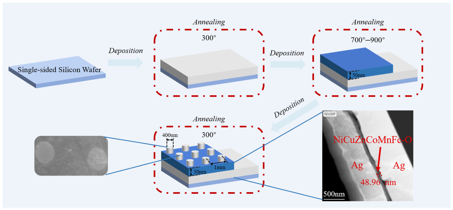
The fabrication process and structural configuration of the Ag/NiCuZnCoMnFe-O/Ag memristive device are schematically illustrated in
Figure 1. Ni
0.3Cu
0.2Zn
0.5Co
0.005Mn
0.005Fe
1.99O precursor powder was first synthesized by a sol–gel method. The obtained powder was subsequently pressed and sintered to prepare a dense ceramic target for pulsed laser deposition (PLD-450).
Single-side polished Si wafers were used as the substrates. Before deposition, the Si substrates were ultrasonically cleaned sequentially in acetone and ethanol for 15 min each, after which they were dried using high-purity N2 gas. A 500 nm-thick Ag bottom electrode was then deposited onto the cleaned Si substrate by electron-beam evaporation. During deposition, the chamber base pressure was maintained at approximately 5 × 10⁻⁴ Pa, the beam current was set to 55 mA, and the deposition rate was controlled at 1.0–1.5 Å s−1. The Ag electrode was annealed at 300 °C for 5 min in vacuum to improve adhesion and electrical contact.
The NiCuZnCoMnFe-O active layer was deposited on the Ag-coated Si substrate by PLD using the prepared ceramic target. The laser energy and repetition rate were fixed at 250 mJ per pulse and 3 Hz, respectively. Deposition was performed under a background vacuum of 1 × 10⁻⁴ Pa, and the thickness of the NiCuZnCoMnFe-O layer was controlled to approximately 50 nm. Measurements from the high-magnification cross-sectional HAADF-STEM image yielded an average film thickness of approximately 48.96 nm. To examine how thermal treatment affects the microstructural features and electronic behavior of the oxide layer, the freshly deposited layers underwent thermal treatment at 700, 800, and 900 °C over a period of 10 min using a vacuum rapid thermal annealing furnace.
Finally, 500-nm-thick Ag top electrodes were deposited onto the NiCuZnCoMnFe-O film through a stencil mask by electron-beam evaporation. The completed Ag/NiCuZnCoMnFe-O/Ag devices were further annealed at 300 °C for 5 min in vacuum to improve the electrical contact between the Ag electrodes and the oxide active layer. As shown in
Figure 1, the resulting device exhibits a typical metal/oxide/metal sandwich structure. The diameter of each circular Ag top electrode is approximately 400 μm, and the spacing between adjacent electrodes is about 1 mm, which ensures sufficient electrical isolation during electrical measurements. The cross-sectional HAADF image further confirms the layered configuration of the device and the formation of a continuous NiCuZnCoMnFe-O active layer between the Ag electrodes.
The surface morphology as a function of annealing temperature, together with the geometry for the device electrodes, was observed using field-emission scanning electron microscopy (CIQTEK DB550, Hefei, China). Cross-sectional TEM specimens were prepared by focused ion beam (FIB) milling. Compositional analysis was conducted via EDS, while local structural features were characterized using cross-sectional HRTEM (an FEI Tecnai F20 system, FEI, Hillsboro, OR, USA). To determine the chemical states of the multicomponent oxide, X-ray photoelectron spectroscopy (XPS, ESCALab250, Thermo Fisher Scientific, Westborough, MA, USA) was employed. Room-temperature magnetic hysteresis loops were measured using a vibrating sample magnetometer (VSM, Model 3100, East Changing Technologies, China/Beijing) under an applied magnetic field of approximately ±12 kOe. The magnetization was normalized to the maximum magnetization value and expressed as M/M_max. A Keithley 4200 semiconductor parameter analyzer (Keithley, Solon, OH, USA) was employed for electronic characterization performed at ambient temperature. During resistive switching and synaptic testing, either bias voltages or pulse stimuli were delivered onto the upper contact, whereas the lower electrode was kept at ground potential. For the pulse measurements, voltage pulses were applied to the Ag top electrode while the bottom electrode was grounded, and the transient current response was recorded to preliminarily evaluate synaptic-like behavior. These measurements were used to examine pulse-induced transient responses rather than to provide a complete conductance-modulation-based synaptic weight-update analysis. I–V characteristics were recorded under bias sweeps reaching a maximum of 0.5 V. The same measurement configuration was used to evaluate the retention behavior, high-resistance state (HRS), low-resistance state (LRS), paired-pulse facilitation (PPF), and pulse-number-dependent response.
3. Results
3.1. Morphology and Microstructure of the Annealed NiCuZnCoMnFe-O Films
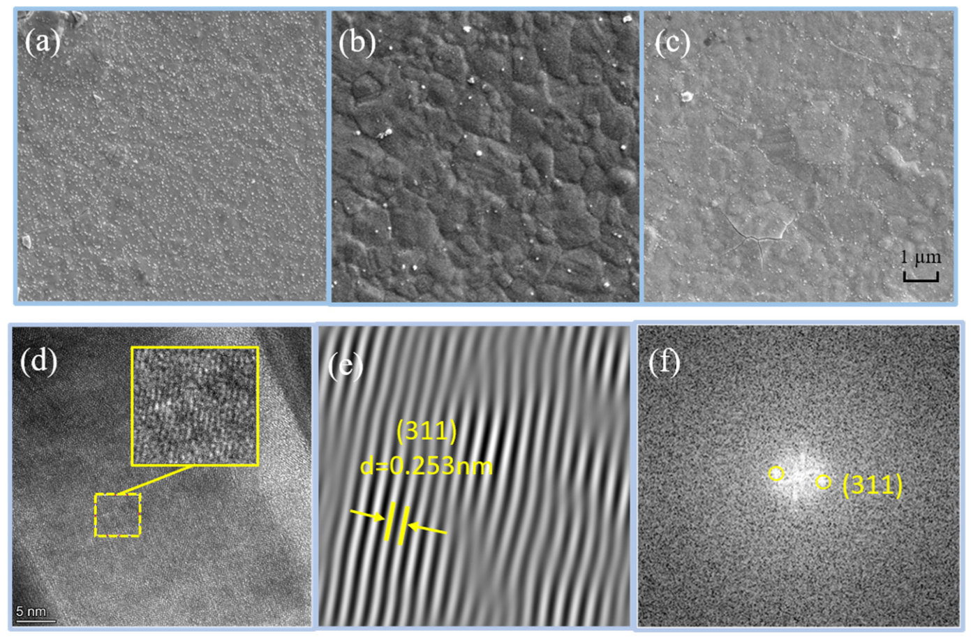
The annealing-temperature-dependent surface morphology and microstructure of the NiCuZnCoMnFe-O thin films are shown in
Figure 2.
Figure 2a–c presents the SEM images of the films annealed at 700, 800, and 900 °C, respectively, recorded at the same magnification of ×10,000 for direct comparison. As shown in
Figure 2a, the film annealed at 700 °C exhibits a continuous surface with numerous fine nanoscale grains, indicating that crystallization has been initiated but remains relatively insufficient. When the annealing temperature is increased to 800 °C, the film surface becomes much denser and more uniform, with clearly developed grains and compact grain boundaries, as shown in
Figure 2b. This suggests that annealing at 800 °C effectively promotes grain growth and microstructural densification while maintaining good film continuity. In contrast, the film annealed at 900 °C shows a rougher surface with locally nonuniform contrast and visible crack-like features, as shown in
Figure 2c. These morphological changes may be associated with excessive grain growth and thermal-stress-induced structural degradation during high-temperature annealing. Therefore, an annealing temperature of 800 °C is more favorable for obtaining a compact and homogeneous NiCuZnCoMnFe-O active layer.
The local crystalline structure of the annealed NiCuZnCoMnFe-O film was further examined by cross-sectional HRTEM. As shown in
Figure 2d, clear lattice fringes can be observed in the selected region, indicating that the oxide film was crystallized after annealing. The enlarged HRTEM image in
Figure 2e shows an interplanar spacing of approximately 0.253 nm, which agrees well with the d-spacing of the spinel ferrite (311) plane listed in PDF#97-010-9045, d(311) = 0.25285 nm. The corresponding FFT pattern in
Figure 2f is also indexed to the (311) reflection. These results confirm that the annealed NiCuZnCoMnFe-O film possesses a spinel-type ferrite structure.
3.2. Elemental Distribution and Chemical States
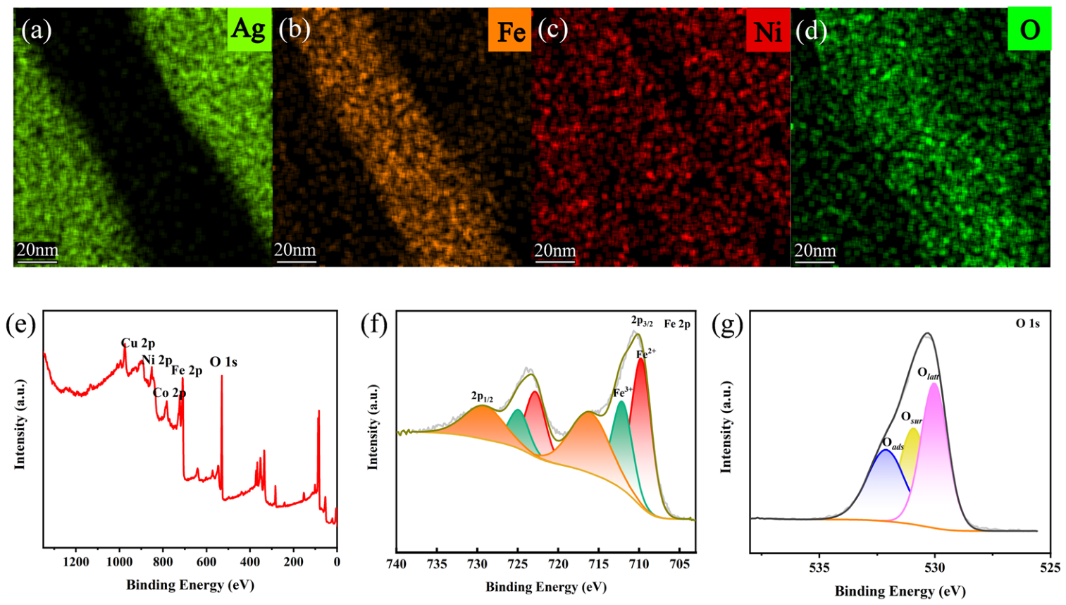
The elemental distribution and chemical states of the NiCuZnCoMnFe-O thin film annealed at 800 °C were further investigated by EDS mapping and XPS, as shown in
Figure 3. The EDS elemental maps in
Figure 3a–d display the spatial distributions of Ag, Fe, Ni, and O in the selected region. A clear contrast can be observed between the Ag electrode and the NiCuZnCoMnFe-O active layer, confirming the formation of the Ag/oxide layered structure. The Fe, Ni, and O signals are continuously distributed within the oxide region, indicating good compositional uniformity of the annealed multicomponent ferrite film. No obvious elemental aggregation or large-scale phase separation is observed, suggesting that the PLD-deposited NiCuZnCoMnFe-O layer maintains a relatively homogeneous elemental distribution after annealing. Such compositional uniformity is beneficial for suppressing uncontrolled local conduction pathways and improving the reproducibility of resistive switching performance.
As illustrated in
Figure 3e, the XPS survey spectrum shows the characteristic signals of Fe, Ni, Cu, Co, and O in the NiCuZnCoMnFe-O film. Combined with the EDS results, these data support the successful formation of the multicomponent oxide layer. To further clarify the valence state of Fe ions, the high-resolution Fe 2p spectrum was deconvoluted, as shown in
Figure 3f. The Fe 2p core-level signal displays two prominent spin–orbit-split doublet features attributable to the Fe 2p
3/
2 and Fe 2p
1/
2 levels, along with accompanying satellite peaks. The fitted components can be assigned to Fe
2+ and Fe
3+ species, confirming the coexistence of mixed Fe valence states in the NiCuZnCoMnFe-O oxide matrix. The Fe
2+/Fe
3+ redox couple can participate in charge compensation and local electron transport, which is favorable for defect-assisted conduction and resistive switching.
The O 1s spectrum in
Figure 3g can be fitted into three components. The peak located at lower binding energy is assigned to lattice oxygen species associated with metal–oxygen bonds in the ferrite oxide framework. The middle component is related to oxygen-deficient regions or surface oxygen species, while the higher-binding-energy component can be attributed to adsorbed oxygen species on the film surface. The presence of non-lattice oxygen components indicates that oxygen vacancies and oxygen-related defects exist in the annealed NiCuZnCoMnFe-O film. These oxygen defects can act as active sites for ion migration and conductive-path evolution under an external electric field. Therefore, the EDS and XPS results demonstrate that the 800-annealed NiCuZnCoMnFe-O film possesses homogeneous elemental distribution, mixed Fe valence states, and oxygen-related defect characteristics, providing an important structural and chemical basis for the low-voltage memristive behavior discussed below. In addition to their role in defect-assisted charge transport, the mixed Fe
2+/Fe
3+ states and oxygen-related defects may also influence magnetic exchange interactions and local spin ordering in the ferrite oxide matrix.
3.3. Magnetic Properties of the Annealed NiCuZnCoMnFe-O Films
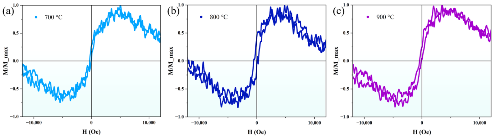
To further evaluate the magnetic characteristics of the annealed NiCuZnCoMnFe-O thin films, room-temperature magnetic hysteresis loops were measured for the samples annealed at 700, 800, and 900 °C, as shown in
Figure 4. Because the magnetic moment of the thin films is relatively weak owing to the small film volume and low mass, the magnetization is normalized by the maximum magnetization value, and the vertical axis is expressed as M/M_max. It should also be noted that the Si substrate contributes a residual diamagnetic background, which results in a non-ideal high-field linear component at both ends of the measured curves. Therefore, the present analysis mainly focuses on the normalized hysteresis behavior and the low-field magnetic response rather than the absolute saturation magnetization.
All three annealed films exhibit clear hysteresis behavior, indicating that the NiCuZnCoMnFe-O films possess room-temperature ferromagnetic/ferrimagnetic characteristics after thermal treatment. The hysteresis loops show finite remanence and coercivity, which can be attributed to the ferrite-type oxide structure containing magnetic transition-metal ions such as Fe, Ni, Co, and Mn. The coexistence of Fe2+/Fe3+ states confirmed by XPS may also contribute to magnetic exchange interactions and defect-related spin ordering in the multicomponent ferrite matrix.
For the film annealed at 700 °C, the hysteresis loop is observable but relatively less regular, suggesting that ferrimagnetic ordering has been established but may still be affected by insufficient crystallization and nanoscale grain development. This is consistent with the SEM observation that the 700-annealed film contains fine grains and relatively incomplete microstructural densification. When the annealing temperature increases to 800 °C, the magnetic hysteresis loop becomes more distinct and better defined, indicating improved magnetic ordering. This behavior can be associated with enhanced crystallinity, compact grain structure, and more homogeneous elemental distribution, which are favorable for stable superexchange interactions among transition-metal cations in the ferrite lattice. Therefore, the 800 °C annealing condition provides a more balanced microstructural and magnetic state for the NiCuZnCoMnFe-O film.
In comparison, the film annealed at 900 °C still shows evident hysteresis behavior, confirming that the ferrimagnetic nature is preserved at the higher annealing temperature. However, the loop shape becomes slightly more fluctuating and the high-field branches remain strongly influenced by the substrate-related background. Combined with the SEM results, the relatively distorted magnetic response of the 900-annealed film may be related to excessive grain growth, increased surface roughness, and crack-like structural features induced by high-temperature annealing. These structural imperfections can introduce nonuniform local stress and defect distribution, thereby affecting the uniformity of magnetic domain rotation and magnetization reversal.
Overall, the magnetic hysteresis results confirm that the annealed NiCuZnCoMnFe-O thin films retain ferrite-type magnetic behavior at room temperature. Among the three annealing temperatures, the 800-annealed film exhibits a relatively well-defined hysteresis response, which agrees with its dense morphology, improved crystallinity, and uniform chemical composition. These results further support that appropriate annealing not only optimizes the microstructure and defect chemistry of the multicomponent ferrite film but also stabilizes its magnetic ordering. Such annealing-dependent magnetic behavior provides additional evidence for the ferrite nature of the active layer and strengthens the structure–property correlation in the Ag/NiCuZnCoMnFe-O/Ag memristive system.
3.4. Resistive Switching Characteristics and Charge Transport Mechanism
The devices annealed at different temperatures were preliminarily evaluated before detailed electrical measurements. The 700-annealed device showed poor memristive behavior because the insufficiently crystallized thin film led to unstable defect migration, a small switching ratio, and poor endurance. The 900-annealed device did not show reliable electrical behavior, probably because high-temperature annealing degraded the Ag electrode continuity and the electrode/oxide interface. Therefore, the 800-annealed device was selected for detailed resistive switching and synaptic measurements because of its improved crystallinity and stable electrode/oxide structure.
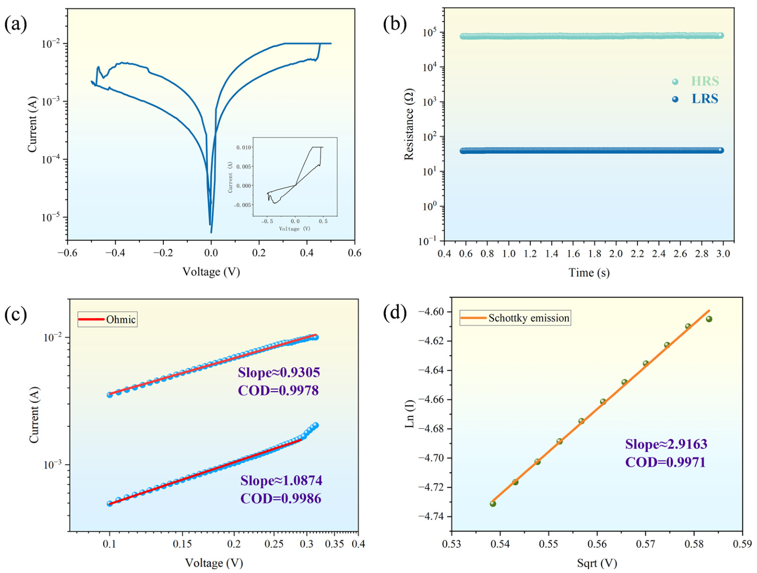
The resistive switching behavior and charge transport mechanism of the Ag/NiCuZnCoMnFe-O/Ag memristive device annealed at 800 °C are illustrated in
Figure 5. A typical pinched hysteresis loop is observed in the I–V curve of the device, as shown in
Figure 5a, confirming its memristive characteristics. During the voltage sweep, the current changes reversibly with the applied bias, indicating the transition between the high-resistance state (HRS) and the low-resistance state (LRS). Notably, the device can be operated within a low voltage range of approximately ±0.5 V, demonstrating its potential for low-power memristive applications. The corresponding I–V curve plotted on a linear scale is shown in the inset of
Figure 5a, further confirming the bipolar resistive switching behavior.
The resistance-state stability of the device was preliminarily examined over a short time scale, as shown in
Figure 5b. The HRS and LRS can still be distinguished during the 3 s measurement, indicating basic short-time resistance-state stability of the optimized 800-annealed device. However, this short retention test is insufficient for evaluating practical nonvolatile memory applications. Therefore, the present result is regarded only as a preliminary short-time stability evaluation rather than a complete long-term retention assessment. Longer retention measurements over extended time scales will be required in future work after further optimization of film crystallinity, electrode continuity, and device stability.
To further understand the charge transport mechanism, the measured I–V curves were fitted using different conduction models. As shown in
Figure 5c, the log–log fitting curves in the LRS exhibit slopes of approximately 0.9305 and 1.0874, which are close to unity. This result indicates that the conduction behavior in the LRS follows an Ohmic transport mechanism. Such Ohmic conduction suggests the formation of oxygen-vacancy-rich conductive paths in the NiCuZnCoMnFe-O active layer. Under the applied electric field, oxygen vacancies migrate and accumulate locally, resulting in the establishment of continuous or nearly continuous defect-assisted conduction channels. These oxygen-vacancy-mediated paths reduce the device resistance and lead to the transition from HRS to LRS.
In contrast, the conduction behavior in the HRS can be well described by the Schottky-emission model, as shown in
Figure 5d. A linear relationship is observed between ln(I) and V
1/2, with a coefficient of determination of 0.9971, indicating that current transport in the HRS is mainly governed by interface-controlled Schottky emission. In this state, the rupture or redistribution of oxygen-vacancy-rich conductive paths increases the effective barrier at the Ag/NiCuZnCoMnFe-O interface, thereby suppressing carrier injection and restoring the device to a high-resistance state. Under an external electric field, modulation of the interfacial barrier caused by oxygen-vacancy redistribution further affects the carrier transport behavior.
Therefore, the resistive switching behavior of the 800-annealed Ag/NiCuZnCoMnFe-O/Ag device can be primarily attributed to the reversible migration, accumulation, and redistribution of oxygen vacancies in the multicomponent ferrite oxide layer, together with the accompanying modulation of the interfacial Schottky barrier. The Ohmic conduction observed in the LRS and the Schottky-emission-dominated transport in the HRS consistently support an oxygen-vacancy-dominated switching mechanism. These results suggest that the annealed NiCuZnCoMnFe-O film provides a favorable defect-chemical environment for representative low-voltage memristive behavior, while further reliability optimization is still needed for stable repeated switching operation.
3.5. Preliminary Synaptic-like Transient Current Responses
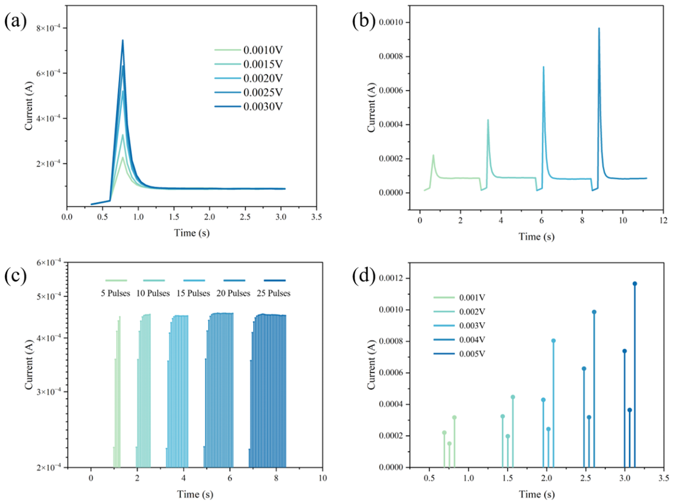
Figure 6 presents preliminary transient current responses of the Ag/NiCuZnCoMnFe-O/Ag device annealed at 800 °C under low-voltage pulse stimulation. As shown in
Figure 6a, the device exhibits current spike-and-relaxation behavior under pulse voltages from 0.0010 to 0.0030 V. The current increases rapidly after the voltage pulse is applied and then gradually decreases after the pulse is removed. The peak current increases with increasing pulse voltage, indicating that the transient response is dependent on the applied stimulus amplitude.
Figure 6b shows the current response under repeated pulse stimulation. Each pulse produces a clear transient current peak followed by a decay process, suggesting that the device can generate repeated pulse-induced current responses under the present measurement conditions. The relaxation after each pulse may be related to the partial redistribution of oxygen vacancies or oxygen-related defects after removal of the electric field. However, because the present measurement mainly records transient current evolution, this result should be regarded as a preliminary indication of volatile response behavior rather than a complete demonstration of synaptic plasticity.
The pulse-number-dependent response is shown in
Figure 6c. As the number of applied pulses increases from 5 to 25, the measured current level gradually increases and then tends to approach a relatively stable range. This behavior suggests that repeated pulse stimulation can induce a cumulative current enhancement in the device. Such accumulation may originate from gradual defect redistribution under consecutive electrical stimuli. Nevertheless, without post-pulse conductance readout and long-time relaxation analysis, the result is more appropriately described as pulse-number-dependent transient current accumulation rather than a definitive short-term-to-long-term memory transition.
Figure 6d presents the response to paired-pulse stimulation under different pulse voltages. For each voltage condition, the second current response is higher than the first one, indicating that the device does not fully return to its initial state before the second pulse is applied. The response amplitude increases with increasing pulse voltage from 0.001 to 0.005 V. This behavior is similar to paired-pulse-facilitation-like current enhancement, but a quantitative PPF index as a function of pulse interval has not yet been obtained. Therefore, the present data only support a preliminary PPF-like response under the selected pulse conditions.
Overall,
Figure 6 indicates that the Ag/NiCuZnCoMnFe-O/Ag device can produce low-voltage transient current responses, including pulse-amplitude-dependent spike currents, repeated spike-and-decay behavior, pulse-number-dependent current accumulation, and paired-pulse-like enhancement. These results provide an initial indication of synaptic-like response features. However, further systematic measurements, including interval-dependent PPF analysis, post-pulse conductance readout, potentiation/depression cycling, endurance, and device-to-device reproducibility, are necessary before making stronger conclusions about neuromorphic synaptic performance.
3.6. Proposed Resistive Switching Mechanism
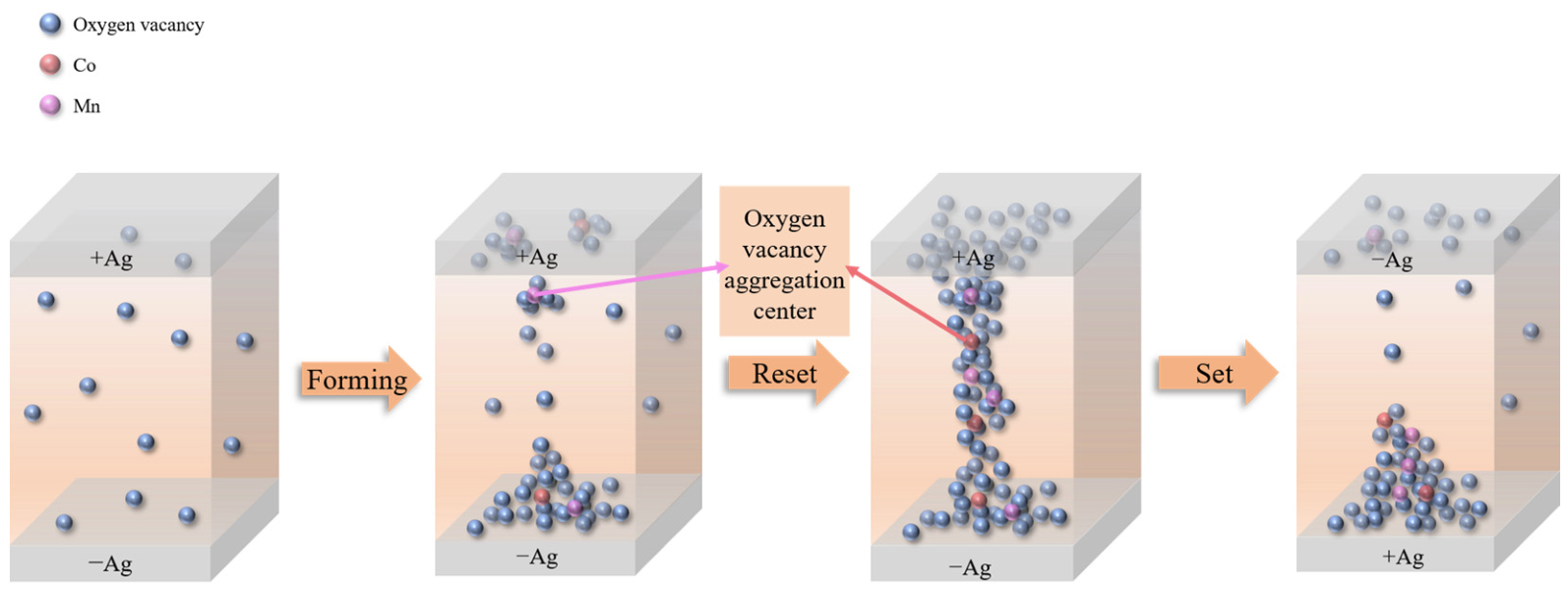
The proposed resistive switching mechanism for the Ag/NiCuZnCoMnFe-O/Ag memristor is schematically depicted in
Figure 7. In the pristine state, oxygen vacancies are randomly dispersed throughout the NiCuZnCoMnFe-O functional layer, and no uninterrupted conductive path exists between the two Ag electrodes. Consequently, the device resides in a high-resistance state, constrained by the limited charge carrier transport across the oxide layer.
During the set process, oxygen vacancies carrying positive charge are driven by the applied electric field to migrate and cluster along the field direction. Owing to the multivalent nature of Co and Mn ions, local defect-rich regions can be generated around Co/Mn-related sites. These regions act as oxygen-vacancy aggregation centers and provide preferential migration paths for vacancy transport. As the oxygen vacancies gradually connect with each other, a localized conductive filament is formed inside the oxide layer, leading to a change in the device state from HRS to LRS.
The reset operation involves the redistribution and partial disruption of the conductive filament. When a reverse electric field is applied, the previously accumulated oxygen vacancies are driven away from the original conductive pathway, resulting in the disconnection of the vacancy-enriched channel. Meanwhile, the interfacial barrier at the Ag/NiCuZnCoMnFe-O interface is restored, which suppresses carrier injection and returns the device to the high-resistance state. This process is consistent with the Schottky-emission-dominated conduction behavior observed in the HRS.
Applying the set voltage again causes oxygen vacancies to re-aggregate near the region enriched with active defects, leading to the reconstruction of the conductive path. The recovery of the vacancy-assisted filament lowers the device resistance and switches it back to the LRS. The Ohmic conduction behavior detected in the low-resistance state provides further evidence for the establishment of either a continuous or a nearly continuous conductive channel.
Therefore, the resistive switching behavior of the Ag/NiCuZnCoMnFe-O/Ag memristor may be ascribed to the reversible formation as well as the disruption of oxygen-vacancy-based conducting paths. The incorporation of Co and Mn may contribute to the regulation of local defect distribution and oxygen-vacancy migration paths. This defect-mediated mechanism explains the low-voltage switching behavior of the device and confirms that the optimized multicomponent oxide layer provides a favorable platform for stable memristive and synaptic functions.
4. Discussion
The present results indicate that post-deposition annealing strongly affects the structure–defect–transport relationship of NiCuZnCoMnFe-O multicomponent ferrite films. Compared with the films annealed at 700 and 900 °C, the 800-annealed film exhibits improved crystallinity, compact morphology, and more uniform elemental distribution. Such a microstructure is beneficial for suppressing uncontrolled leakage paths and stabilizing oxygen-vacancy migration, thereby leading to more reliable low-voltage resistive switching. The XPS results further confirm the coexistence of Fe2+/Fe3+ states and oxygen-related defects, which provide a chemical basis for charge compensation, defect-assisted transport, and resistance modulation.
The electrical switching behavior can be mainly explained by oxygen-vacancy migration coupled with interfacial Schottky barrier modulation. The Ohmic conduction observed in the LRS suggests the formation of vacancy-assisted conductive paths, whereas the Schottky-emission behavior in the HRS indicates that carrier injection is limited by the Ag/NiCuZnCoMnFe-O interface after redistribution or partial rupture of these paths. Although possible Ag-related ionic effects cannot be completely excluded, the combined XPS and conduction-fitting results suggest that oxygen vacancies play the dominant role in the observed switching process. It should be noted that the present electrical results mainly demonstrate the representative switching behavior of the optimized 800-annealed device. More systematic cycle-to-cycle reproducibility, device-to-device uniformity, and endurance measurements will be useful for further evaluating the reliability of this device system.
The pulse-response measurements are also generally consistent with this defect-mediated interpretation. Under pulse stimulation, oxygen-related defects may be locally redistributed, producing transient current enhancement and relaxation. The observed spike-and-decay behavior, voltage-dependent peak current, pulse-number-dependent current accumulation, and paired-pulse-like enhancement suggest preliminary synaptic-like response features. Further quantitative analyses of synaptic characteristics, including interval-dependent PPF, conductance modulation, potentiation/depression behavior, and long-term relaxation, will be carried out in future work. The magnetic measurements confirm the ferrite-type magnetic behavior of the annealed films. However, the direct relationship between magnetic ordering and resistive switching has not yet been established. Magnetic-field-dependent electrical measurements are therefore required in future work to further clarify possible coupling among magnetic ordering, defect migration, and interfacial transport. Therefore, magnetic-field-dependent electrical measurements could be further carried out in future work to clarify whether magnetic ordering influences defect migration, interfacial transport, and resistive switching behavior in this multicomponent ferrite memristive system.