
Design of a 2–4 Decoder Based on All-Spin Logic and Magnetic Tunnel Junction


Abstract
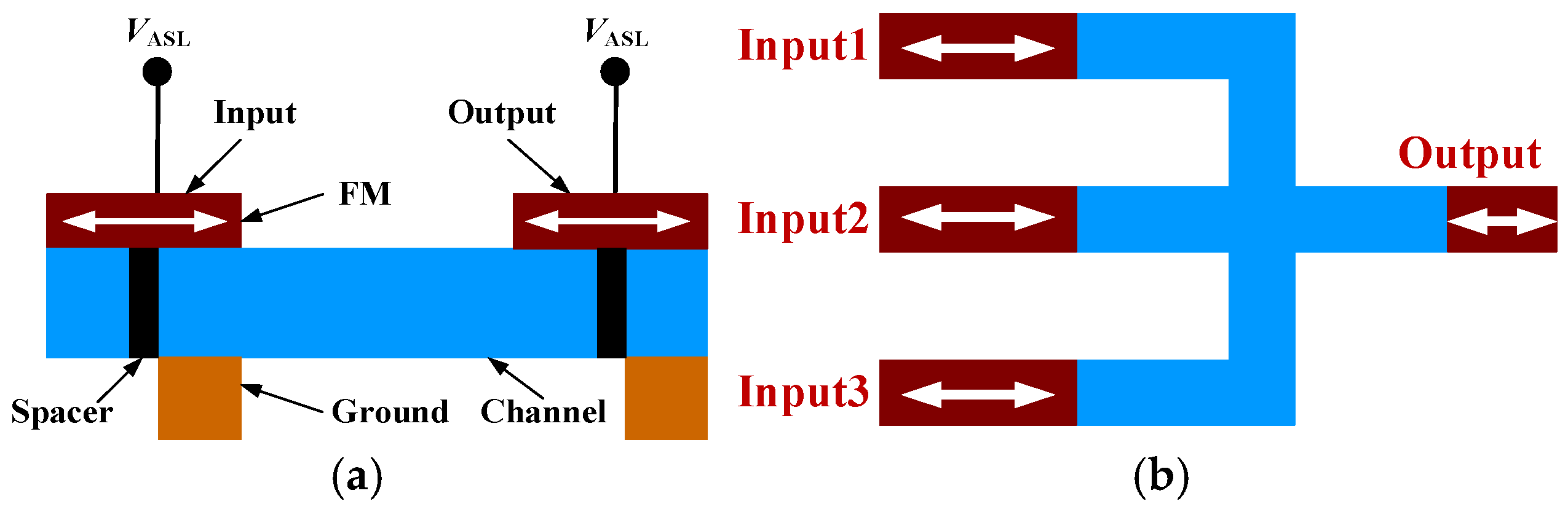
1. Introduction
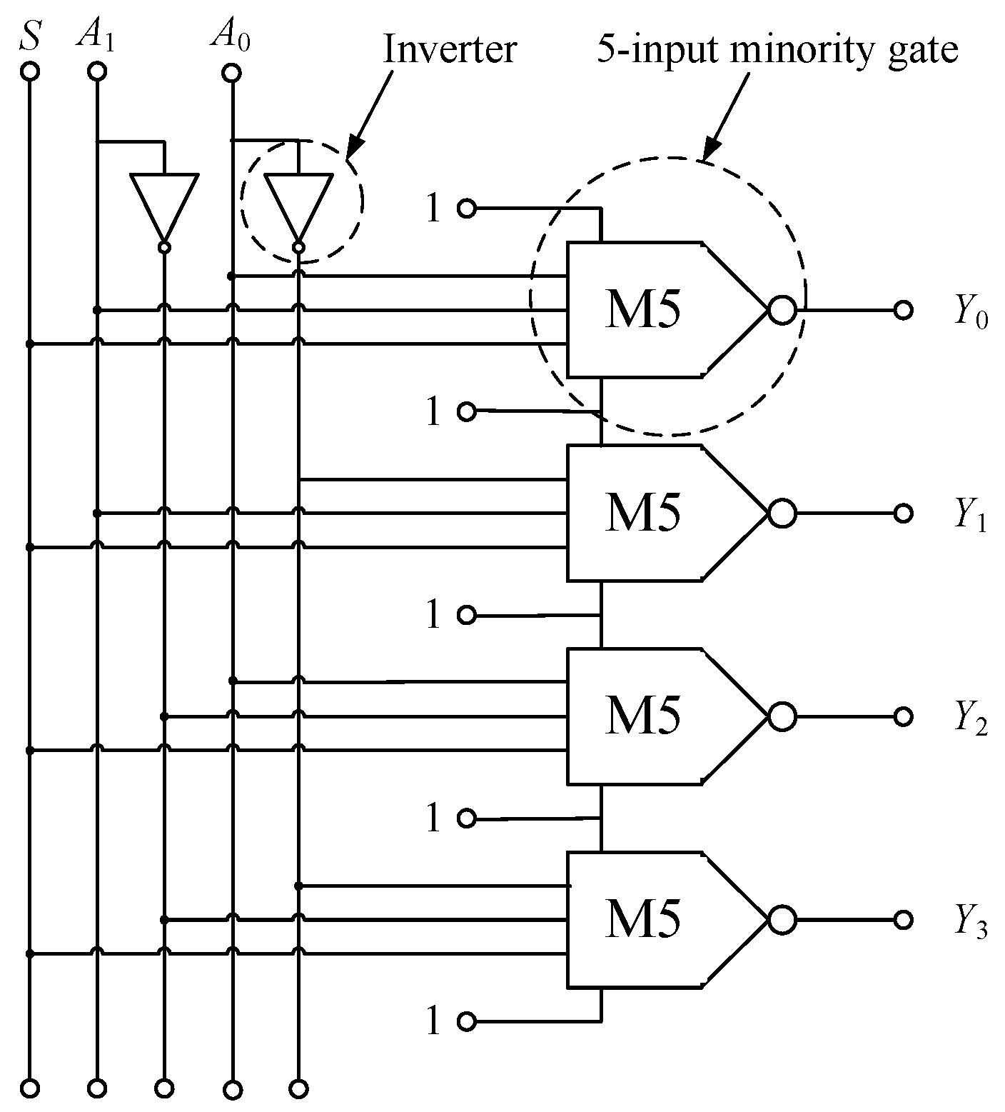
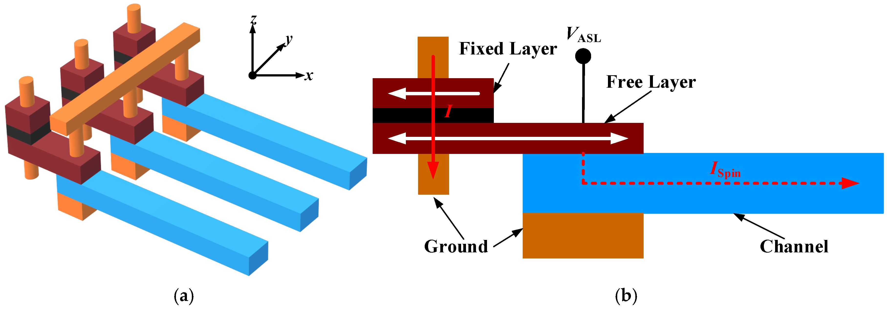
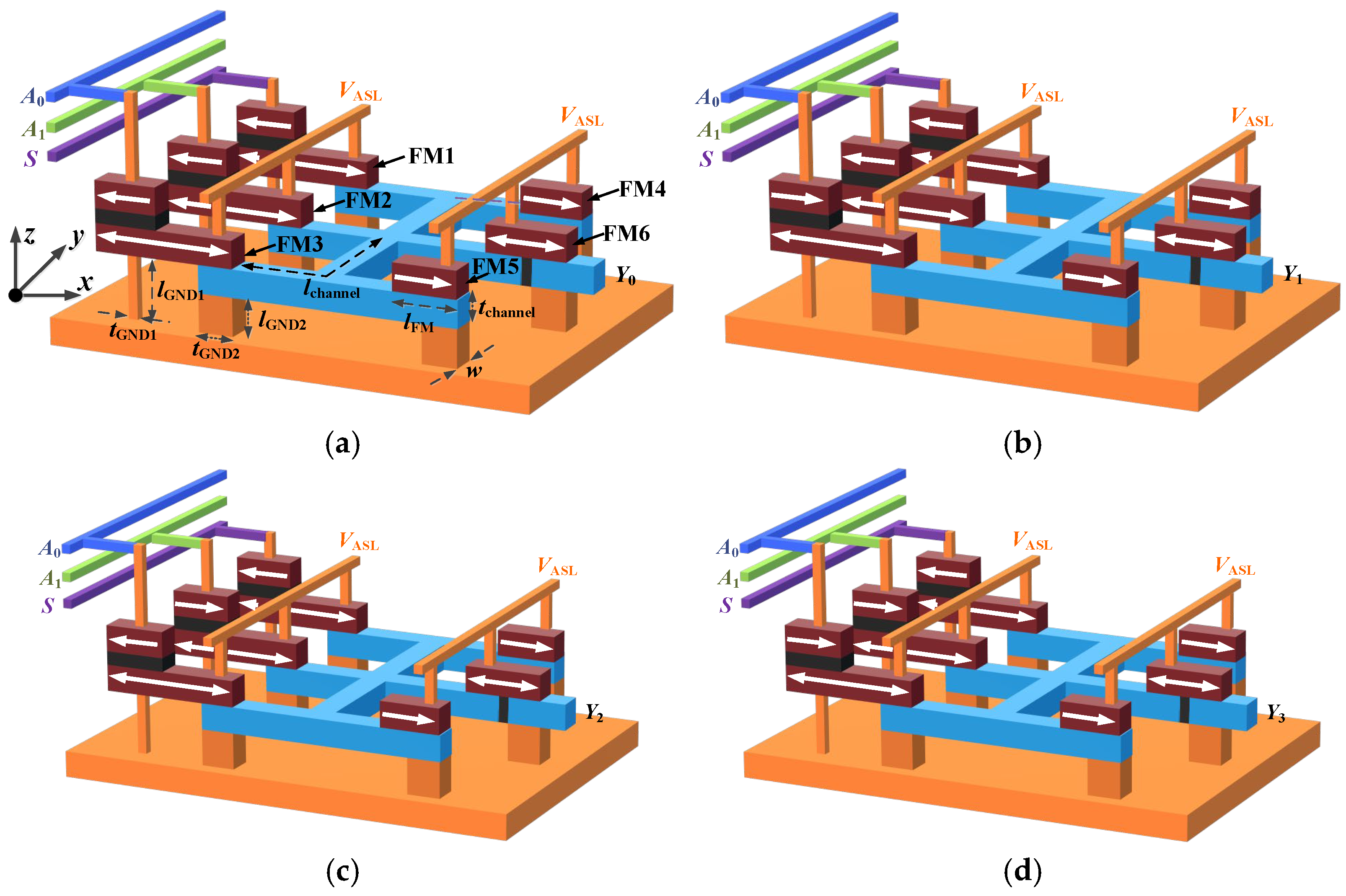
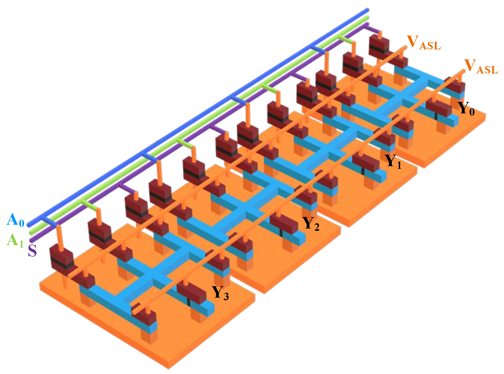
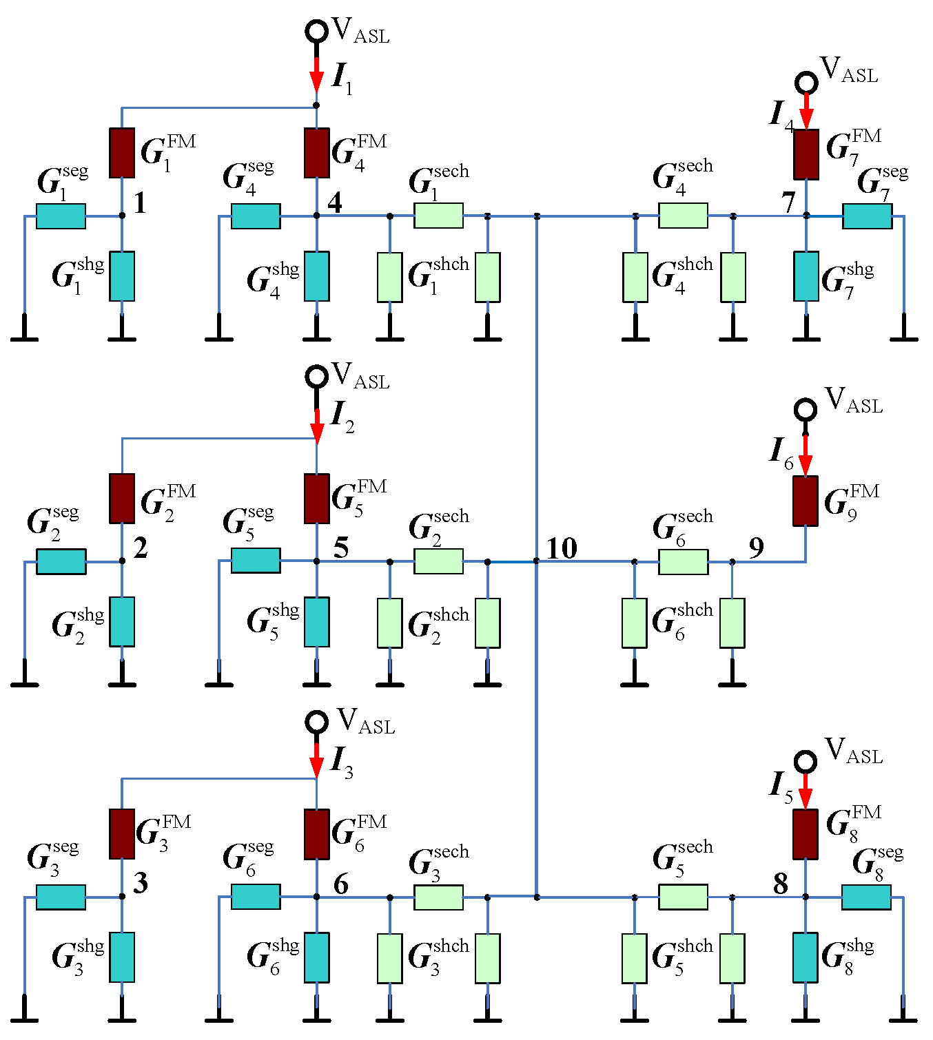
2. Design of the Proposed 2–4 Decoder
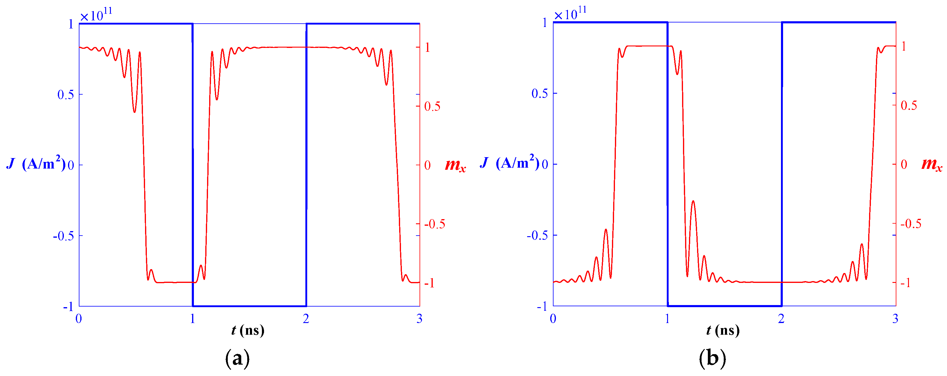
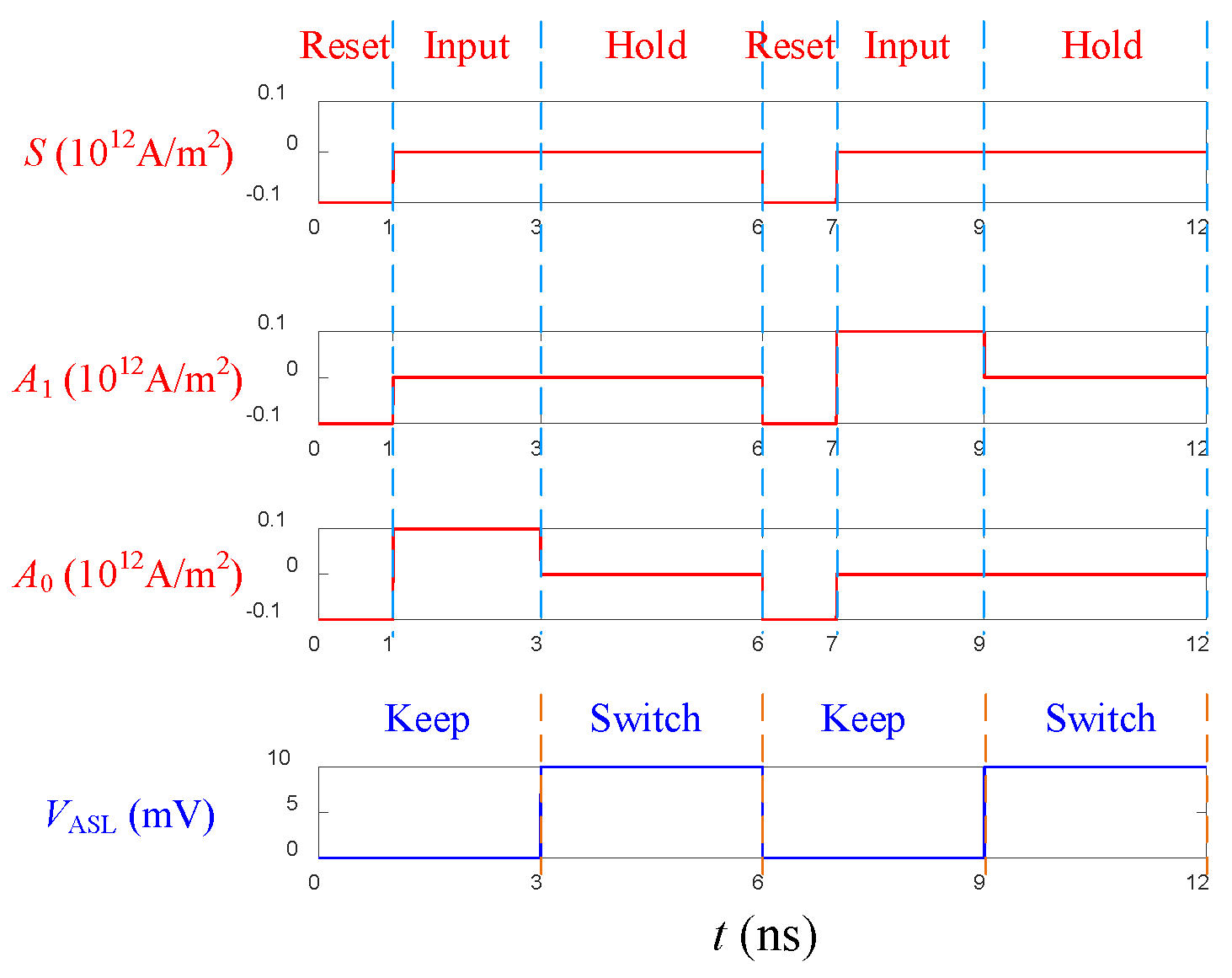
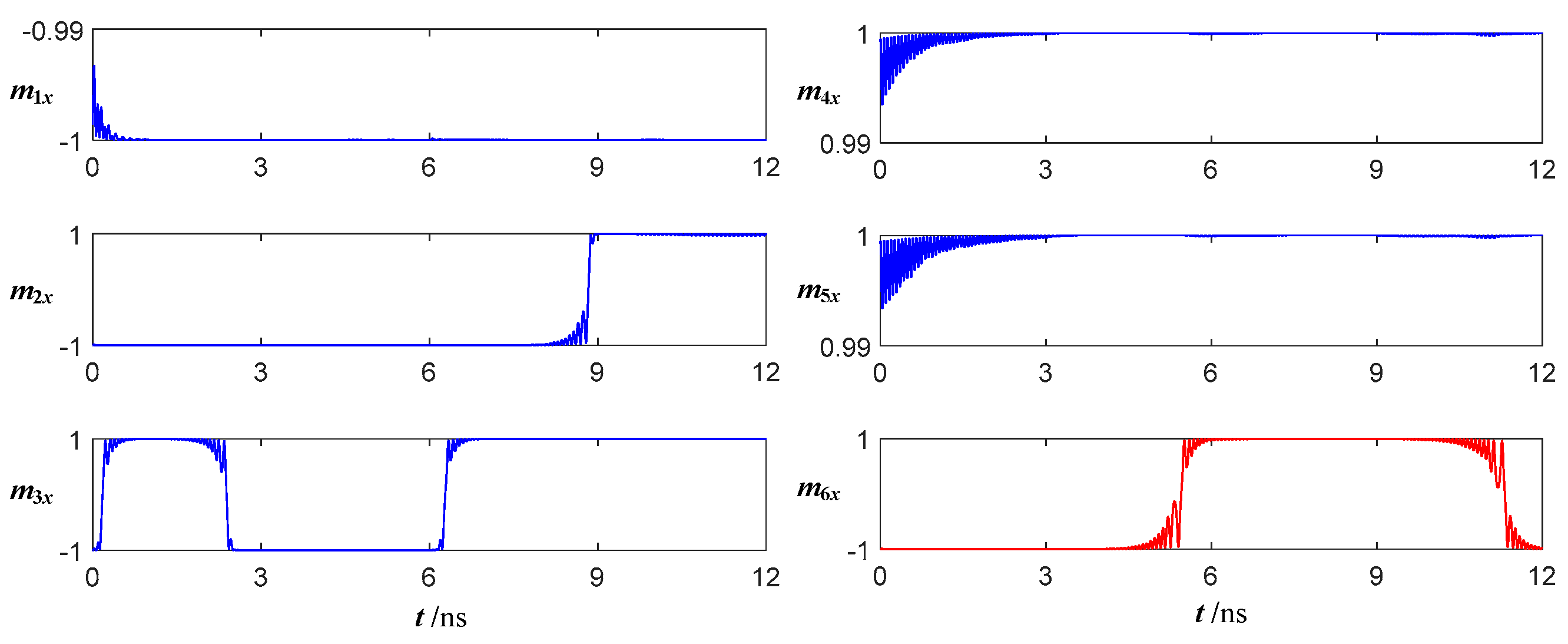
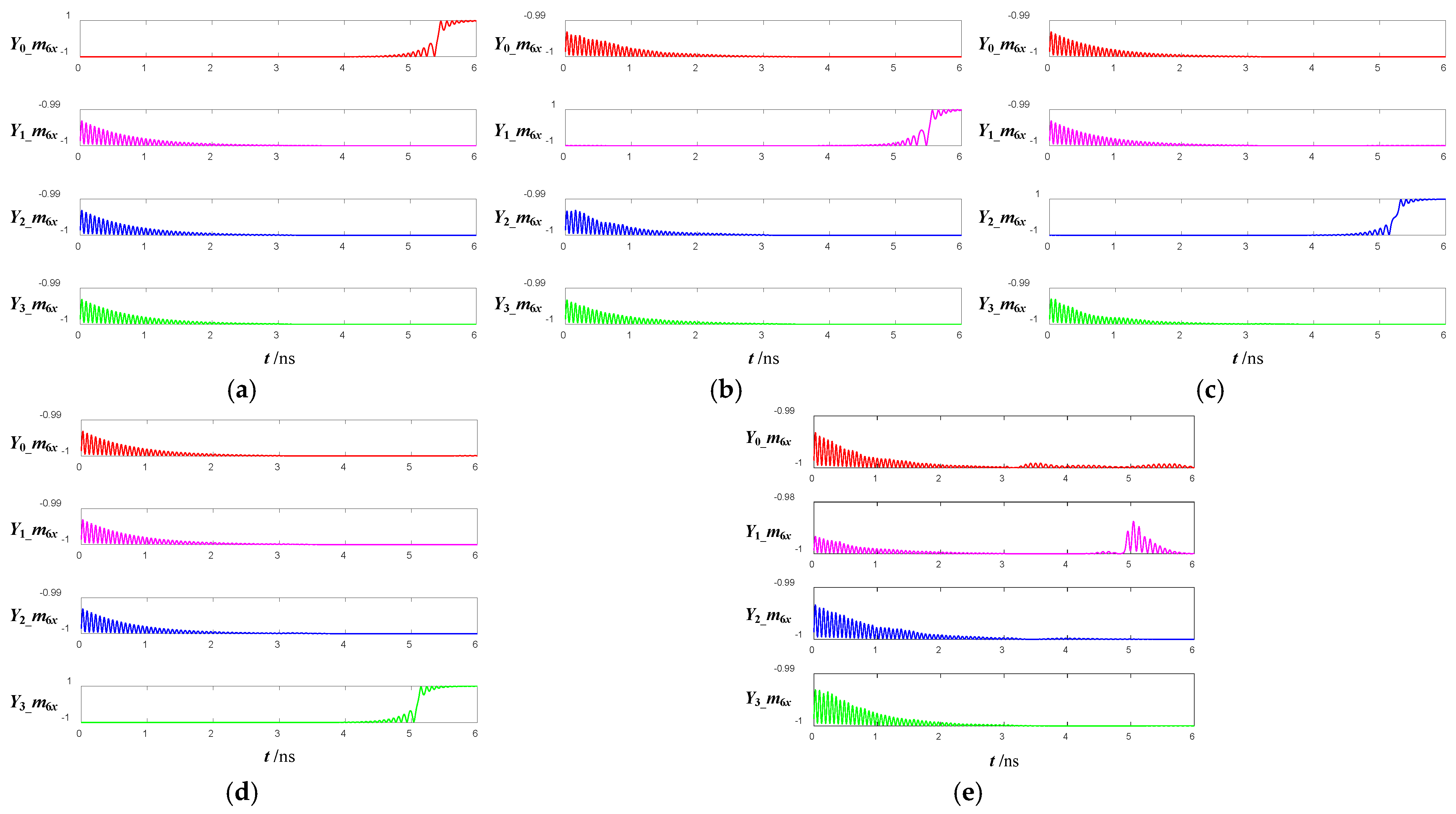
3. Functional Verification of the 2–4 Decoder
4. The Results and Discussions
5. Conclusions
Author Contributions
Funding
Data Availability Statement
Conflicts of Interest
References
- Rajput, P.J.; Bhandari, S.U.; Wadhwa, G. A review on—Spintronics an emerging technology. Silicon 2022, 14, 9195–9210. [Google Scholar] [CrossRef]
- Yakout, S.M. Spintronics: Future technology for new data storage and communication devices. J. Supercond. Nov. Magn. 2020, 33, 2557–2580. [Google Scholar] [CrossRef]
- Hu, G.; Xiang, B. Recent advances in two-dimensional spintronics. Nanoscale Res. Lett. 2020, 15, 226. [Google Scholar] [CrossRef]
- Liu, Y.; Zeng, C.; Zhong, J.; Ding, J.; Wang, Z.M.; Liu, Z. Spintronics in two-dimensional materials. Nano-Micro Lett. 2020, 12, 93. [Google Scholar] [CrossRef] [PubMed]
- Dattagupta, S. Two-dimensional spintronics in a magnetic field—An overview of salient theory. Pramana—J. Phys. 2022, 96, 23. [Google Scholar] [CrossRef]
- Hirohata, A.; Yamada, K.; Nakatani, Y.; Prejbeanu, I.L.; Diény, B.; Pirro, P.; Hillebrands, B. Review on spintronics: Principles and device applications. J. Magn. Magn. Mater. 2020, 509, 166711. [Google Scholar] [CrossRef]
- Barla, P.; Joshi, V.K.; Bhat, S. Spintronic devices: A promising alternative to CMOS devices. J. Comput. Electron. 2021, 20, 805–837. [Google Scholar] [CrossRef]
- Sugahara, S.; Tanaka, M. A spin metal–oxide–semiconductor field effect transistor using half-metallic-ferromagnet contacts for the source and drain. Appl. Phys. Lett. 2004, 84, 2307–2309. [Google Scholar] [CrossRef]
- Cowburn, R.P.; Welland, M.E. Room temperature magnetic quantum cellular automata. Science 2000, 287, 1466–1468. [Google Scholar] [CrossRef] [PubMed]
- Allwood, D.A.; Xiong, G.; Faulkner, C.C.; Atkinson, D.; Petit, D.; Cowburn, R.P. Magnetic domain-wall logic. Science 2005, 309, 1688–1692. [Google Scholar] [CrossRef]
- Behin-Aein, B.; Datta, D.; Salahuddin, S.; Datta, S. Proposal for an all-spin logic device with built-in memory. Nat. Nanotechnol. 2010, 5, 266–270. [Google Scholar] [CrossRef] [PubMed]
- Khitun, A.; Wang, K.L. Nano scale computational architectures with spin wave bus. Superlatt. Microstruct. 2005, 38, 184–200. [Google Scholar] [CrossRef]
- Nikonov, D.E.; Bourianoff, G.I. Spin gain transistor in ferromagnetic semiconductors: The semiconductor Bloch equations approach. IEEE Trans. Nanotechnol. 2005, 4, 206–214. [Google Scholar] [CrossRef]
- Chang, S.C.; Kani, N.; Manipatruni, S.; Nikonov, D.E.; Young, I.A.; Naeemil, A. Scaling limits on all-spin logic. IEEE Trans. Magn. 2016, 52, 3400404. [Google Scholar] [CrossRef]
- Su, L.; Zhao, W.S.; Zhang, Y.; Querlioz, D.; Zhang, Y.G.; Klein, J.O.; Dollfus, P.; Bournel, A. Proposal for a grapheme-based all-spin logic gate. Appl. Phys. Lett. 2015, 106, 072407. [Google Scholar] [CrossRef]
- Zhang, Z.Z.; Zhang, Y.; Zheng, Z.Y.; Wang, G.D.; Su, L.; Zhang, Y.G.; Zhao, W.S. Energy consumption analysis of graphene based all spin logic device with voltage controlled magnetic anisotropy. AIP Adv. 2017, 7, 055925. [Google Scholar] [CrossRef]
- Wang, S.; Cai, L.; Qi, K.; Yang, X.K.; Feng, C.W.; Cui, H.Q. Impact of nanomagnets size on switching behavior of all spin logic devices. Micro Nano Lett. 2016, 11, 508–513. [Google Scholar] [CrossRef]
- Manipatruni, S.; Nikonov, D.E.; Young, I.A. Material targets for scaling all-spin logic. Phys. Rev. Appl. 2016, 5, 014002. [Google Scholar] [CrossRef]
- Zhang, Y.; Zhang, Z.Z.; Wang, L.Z.; Nan, J.; Zheng, Z.Y.; Li, X.; Wong, K.; Wang, Y.; Klein, J.O.; Amiri, P.K.; et al. Partial spin absorption induced magnetization switching and its voltage-assisted improvement in an asymmetrical all spin logic device at the mesoscopic scale. Appl. Phys. Lett. 2017, 111, 052407. [Google Scholar] [CrossRef]
- Iraei, R.M.; Kani, N.; Dutta, S.; Nikonov, D.E.; Manipatruni, S.; Young, I.A.; Heron, J.T.; Naeemi, A. Clocked magnetostriction-assisted spintronic device design and simulation. IEEE Trans. Electron. Devices 2018, 65, 2040–2046. [Google Scholar] [CrossRef]
- Gao, T.Q.; Zeng, L.; Zhang, D.M.; Qin, X.W.; Long, M.Z.; Zhang, Y.; Lin, X.Y.; Zhang, Y.G.; Zhao, W.S. Negative capacitance enhanced all spin logic devices with an ultra-low 1 mV working voltage. IEEE J. Electron. Devices 2018, 6, 245–249. [Google Scholar] [CrossRef]
- Hassan, N.; Saha, D.; Linseisen, C.M.; Vyas, V.; Friedman, J.S. Energy efficiency challenges for all-spin logic. Microelectron. J. 2021, 110, 105008. [Google Scholar] [CrossRef]
- Patra, M.; Maiti, S.K. All-spin logic operations: Memory device and reconfigurable computing. Europhys. Lett. 2018, 121, 38004. [Google Scholar] [CrossRef]
- An, Q.; Beux, S.L.; O’Connor, I.; Klein, J.O. A comprehensive compact model for the design of all-spin-logic based circuits. Microelectron. J. 2019, 92, 104442.1–104442.10. [Google Scholar] [CrossRef]
- Calayir, V.; Nikonov, D.E.; Manipatruni, S.; Young, I.A. Static and clocked spintronic circuit design and simulation with performance analysis relative to CMOS. IEEE Trans. Circuits Syst. I 2014, 61, 393–406. [Google Scholar] [CrossRef]
- Augustine, C.; Panagopoulos, G.; Behin-Aein, B.; Srinivasan, S.; Sarkar, A.; Roy, K. Low-power functionality enhanced computation architecture using spin-based devices. In Proceedings of the 2011 IEEE/ACM International Symposium on Nanoscale Architectures, San Diego, CA, USA, 8–9 June 2011. [Google Scholar] [CrossRef]
- Wang, S.; Cai, L.; Feng, C.W.; Cui, H.Q.; Yang, X.K.; Zhao, H.Y. RS flip-flop implementation based on all spin logic devices. Micro Nano Lett. 2017, 12, 396–400. [Google Scholar] [CrossRef]
- Wang, S.; Yang, Y.; Song, W.B.; Cui, H.Q.; Li, C.; Cai, L. All-spin logic XOR gate implementation based on input interface. IET Circuits Device Syst. 2019, 13, 607–613. [Google Scholar] [CrossRef]
- Wang, S.; Zhang, Y.F.; Wang, X.Y.; Cong, G.T.; Zhang, X.X. Proposal for an input interface and multi output structures of all-spin logic circuits based on magnetic tunnel junction. IET Circuits Device Syst. 2020, 14, 838–845. [Google Scholar] [CrossRef]
- Manipatruni, S.; Nikonov, D.E.; Young, I.A. Modeling and design of spintronic integrated circuits. IEEE Trans. Circuits Syst. I Reg. Pap. 2012, 59, 2801–2814. [Google Scholar] [CrossRef]
- Kuboki, K.; Takahashi, H. Spontaneous spin current near the interface between unconventional superconductors and ferromagnets. Phys. Rev. B 2004, 70, 214524. [Google Scholar] [CrossRef]
- Kuboki, K.; Yano, K. Microscopic Derivation of Ginzburg–Landau Equations for Coexistent States of Superconductivity and Magnetism. J. Phys. Soc. Jpn. 2012, 81, 064711. [Google Scholar] [CrossRef]


| S | A1 | A0 | Y3 | Y2 | Y1 | Y0 |
|---|---|---|---|---|---|---|
| 1 | × | × | 0 | 0 | 0 | 0 |
| 0 | 0 | 0 | 0 | 0 | 0 | 1 |
| 0 | 0 | 1 | 0 | 0 | 1 | 0 |
| 0 | 1 | 0 | 0 | 1 | 0 | 0 |
| 0 | 1 | 1 | 1 | 0 | 0 | 0 |
| Parameters | Description | Values | Parameters | Description | Values |
|---|---|---|---|---|---|
| lFM_L (nm) | length of FM 1, 2, and 3 | 100 | Gilbert damping constant of Py | 0.007 | |
| lFM_R (nm) | length of FM 4, 5, and 6 | 50 | TMR asymmetry parameter | 4 | |
| lFM_F (nm) | length of MTJ fixed layers | 40 | (nm) | spin flip length of Cu | 350 |
| lchannel_L (nm) | length of channel 1, 3, 4, and 5 | 250 | T (K) | Kelvin temperature | 300 |
| lchannel_S (nm) | length of channels 2 and 6 | 200 | spin polarization efficiency constant | 0.35 | |
| lGND1 (nm) | length of MTJ GND | 70 | () | resistivity of Cu | 34 |
| tchannel (nm) | thickness of channel | 50 | (A·m−1) | saturation magnetization of Py | |
| tFM (nm) | thickness of FMs | 0.8 | TMR | tunnel magneto-resistance of MTJ | 10% |
| tGND1 (nm) | thickness of MTJ GND | 20 | uniaxial anisotropy parameter for FMs | ||
| tGND2 (nm) | thickness of minority GND | 40 | Nd1 | demagnetizing tensor for FM1~3 | [0.012 0.041 0.947] |
| w(nm) | width of device | 30 | Nd2 | demagnetizing tensor for FM4~6 | [0.023 0.039 0.938] |
| lGND2 (nm) | length of minority GND | 20 | RA () | resistance area product of MTJ |
| SA1A0 | (pJ) | (pJ) | SA1A0 | (pJ) | (pJ) |
|---|---|---|---|---|---|
| 000 | 0.116 | 9.299 | 100 | 0.194 | 9.297 |
| 001 | 0.195 | 9.299 | 101 | 0.272 | 9.297 |
| 010 | 0.195 | 9.299 | 110 | 0.272 | 9.296 |
| 011 | 0.273 | 9.299 | 111 | 0.351 | 9.297 |
| Performance | First Decoder | Second Decoder |
|---|---|---|
| Maximum channel length (nm) | 250 | 1430 |
| Total length of channels (nm) | 5200 | 12,740 |
| Number of FMs | 36 | 26 |
| Layout area (um2) | 0.319 | 0.841 |
| Number of clock cycles | 1 | 3 |
Disclaimer/Publisher’s Note: The statements, opinions and data contained in all publications are solely those of the individual author(s) and contributor(s) and not of MDPI and/or the editor(s). MDPI and/or the editor(s) disclaim responsibility for any injury to people or property resulting from any ideas, methods, instructions or products referred to in the content. |
© 2025 by the authors. Licensee MDPI, Basel, Switzerland. This article is an open access article distributed under the terms and conditions of the Creative Commons Attribution (CC BY) license (https://creativecommons.org/licenses/by/4.0/).
Share and Cite
Wang, S.; Zhang, Y.; Shan, D. Design of a 2–4 Decoder Based on All-Spin Logic and Magnetic Tunnel Junction. Magnetochemistry 2025, 11, 17. https://doi.org/10.3390/magnetochemistry11020017
Wang S, Zhang Y, Shan D. Design of a 2–4 Decoder Based on All-Spin Logic and Magnetic Tunnel Junction. Magnetochemistry. 2025; 11(2):17. https://doi.org/10.3390/magnetochemistry11020017
Chicago/Turabian StyleWang, Sen, Yongfeng Zhang, and Dan Shan. 2025. "Design of a 2–4 Decoder Based on All-Spin Logic and Magnetic Tunnel Junction" Magnetochemistry 11, no. 2: 17. https://doi.org/10.3390/magnetochemistry11020017
APA StyleWang, S., Zhang, Y., & Shan, D. (2025). Design of a 2–4 Decoder Based on All-Spin Logic and Magnetic Tunnel Junction. Magnetochemistry, 11(2), 17. https://doi.org/10.3390/magnetochemistry11020017