Abstract
A 2–4 decoder based on all-spin logic (ASL) and magnetic tunnel junction (MTJ) is proposed. The decoder employs five-input minority gates to realize three-input NOR gates, which reduces the circuit size compared to the three-input minority gates. Simultaneously, the inputs of the original and reverse variables are implemented by initializing the MTJ fixed layer magnetization in different directions, which avoids the use of inverters. In addition, the 2–4 decoder adopts a single-input single-fan-out (SISF) structure, which reduces the channel length. To illustrate the advantages of the five-input minority gate, inverter-free structure, and SISF structures in designing the proposed 2–4 decoder, a second 2–4 decoder is proposed that uses three-input minority gates, inverters, and a single-input multiple-fan-out structure. Compared with the second decoder, the first decoder has the layout area reduced to 37.9%, the total channel length reduced to 40.8%, and the number of clock cycles reduced to one-third. Importantly, the design methods used in this work, such as multi-input minority gates, SISF structure, and inverter-free structure, provide an interesting approach for designing large-scale ASL logic circuits.
1. Introduction
As CMOS technology approaches its physical limits, many researchers are beginning to explore alternative technologies. Spin-based devices possess the advantages of robustness, ultra-low power consumption, and non-volatility, and are likely to become important candidates in the post-CMOS era [1,2,3,4,5,6,7]. Many spin-based devices have been proposed, such as spin field-effect transistors [8], nanomagnetic logic [9], magnetic domain wall logic [10], all-spin logic (ASL) [11], spin-wave-bus devices [12], spin gain transistors [13], etc.
In particular, ASL does not require additional hardware for repeated spin-charge conversion, which has attracted considerable attention [14,15,16,17,18,19,20,21,22,23,24]. Various types of logic circuits based on ASL have been proposed, such as inverter, majority/minority gate [11], D flip-flop [25], full adder [26], RS flip-flop [27], and XOR gate [28]. However, as an important element in logic circuits, the decoder has not been reported in the public as much as we know. A possible reason for this is as follows: decoders are medium-scale circuits that require the combination of several basic logic gates through non-magnetic channels, which usually require long channels to transmit spin information. However, due to the dramatic dissipation of the spin current in the channel, the use of long channels will offset any possible advantage and even cause the circuit to malfunction.
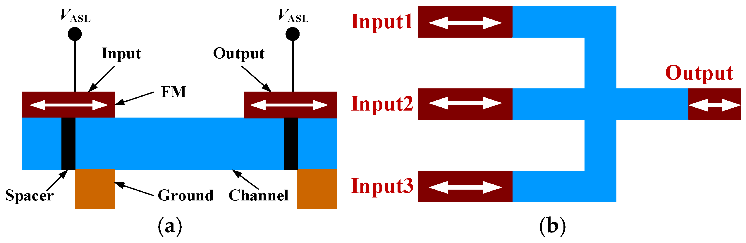
In addition, ASL circuits use the magnetization direction to represent binary information, so it is necessary to initialize the magnetization direction to determine the initial values of ASL circuits. Ref. [29] proposed a single-input single-fan-out (SISF) structure based on a magnetic tunnel junction (MTJ) to provide input signals for ASL circuits. The SISF structure can reduce the channel length in large-scale ASL circuits with multiple identical inputs, which in turn reduces the dissipation of spin current in the channel.
Unlike traditional CMOS technology, the basic logic gates in ASL circuits are no longer NAND/NOR gates but inverter/buffer and majority/minority gates, as shown in Figure 1. Each device consists of four parts, namely a ferromagnet (FM), channel, spacer, and ground. The magnetization of every FM has two stable states representing binary data, “1” and “0”, respectively. If the polarity of the supply voltage VASL is positive, as in Figure 1a, the magnetization direction of the output FM will be opposite to the magnetization of the input FM, and the inverter can be realized [11]. In Figure 1b, the magnetization direction of the output FM will be opposite to the majority of the magnetization directions of the three input FMs; that is, the minority gate is realized [27].
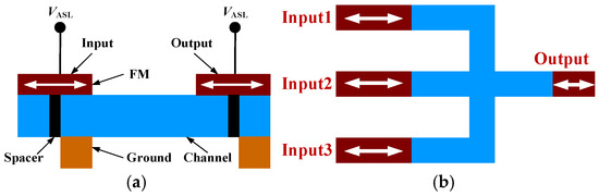
Figure 1.
Layout of ASL circuits: (a) main view of an inverter; (b) top view of a 3-input minority gate.
Based on the three-input minority gate as shown in Figure 1b, a two-input NOR gate can be implemented [27]. However, it would be more convenient to implement a 2–4 decoder using three-input NOR gates. Therefore, it is necessary to use a five-input minority gate to implement three-input NOR gates. Inspired by the above analysis, a 2–4 decoder based on ASL is proposed, which employs SISF structure and five-input minority gates.
2. Design of the Proposed 2–4 Decoder
The truth table of a 2–4 decoder is shown in Table 1. The decoder has an enable terminal S, two inputs A1 and A0, and four outputs Y0~Y3.

Table 1.
The truth table of 2–4 decoder.
According to Table 1, the expressions for each output can be written as follows:
Moreover, if two inputs are set to 1, the expression for the 5-input minority gate becomes
and the 3-input NOR logic function is realized. Therefore, to realize Y0 to Y3 with 5-input minority gates, the expression for Y0 to Y3 can be written as follows:
According to the Equation (3), the schematic of the 2–4 decoder is shown in Figure 2.
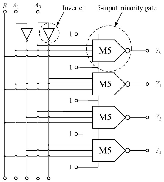
Figure 2.
Schematic of 2–4 decoder based on inverter and 5-input minority gate.
As shown in Figure 2, the 2–4 decoder consists of four 5-input minority gates, two inverters, and several connecting lines. Additionally, there are several minority gates that share the same input signal. In ASL circuits, a common method is to use channels to connect input ports and minority gates, resulting in the use of long channels to transmit spin signals. However, as the length of the channel increases, the spin current decays exponentially, leading to a large increase in energy dissipation. In particular, when the length of the channel exceeds the spin diffusion length, the spin current cannot effectively rotate the magnetization direction of the FM.
Moreover, it is necessary to initialize the magnetization direction of FMs in ASL circuits. To avoid the use of long channels and to initialize the magnetization direction of the 2–4 decoder, an SISF structure is used, as shown in Figure 3a. Here, an MTJ is used to realize the charge-to-spin conversion, and there is only one fan-out for each input. Figure 3b is the front view of Figure 3a. The white arrow indicates the magnetization direction of the FMs, where the magnetization direction of the fixed layer remains unchanged, while the magnetization direction of the free layer is determined by the polarity of current I.
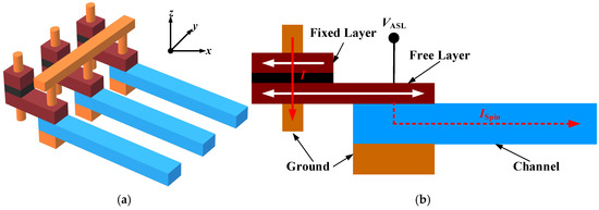
Figure 3.
Schematic of SISF structure: (a) three-dimensional schematic diagram of SISF structure; (b) front view of SISF structure.
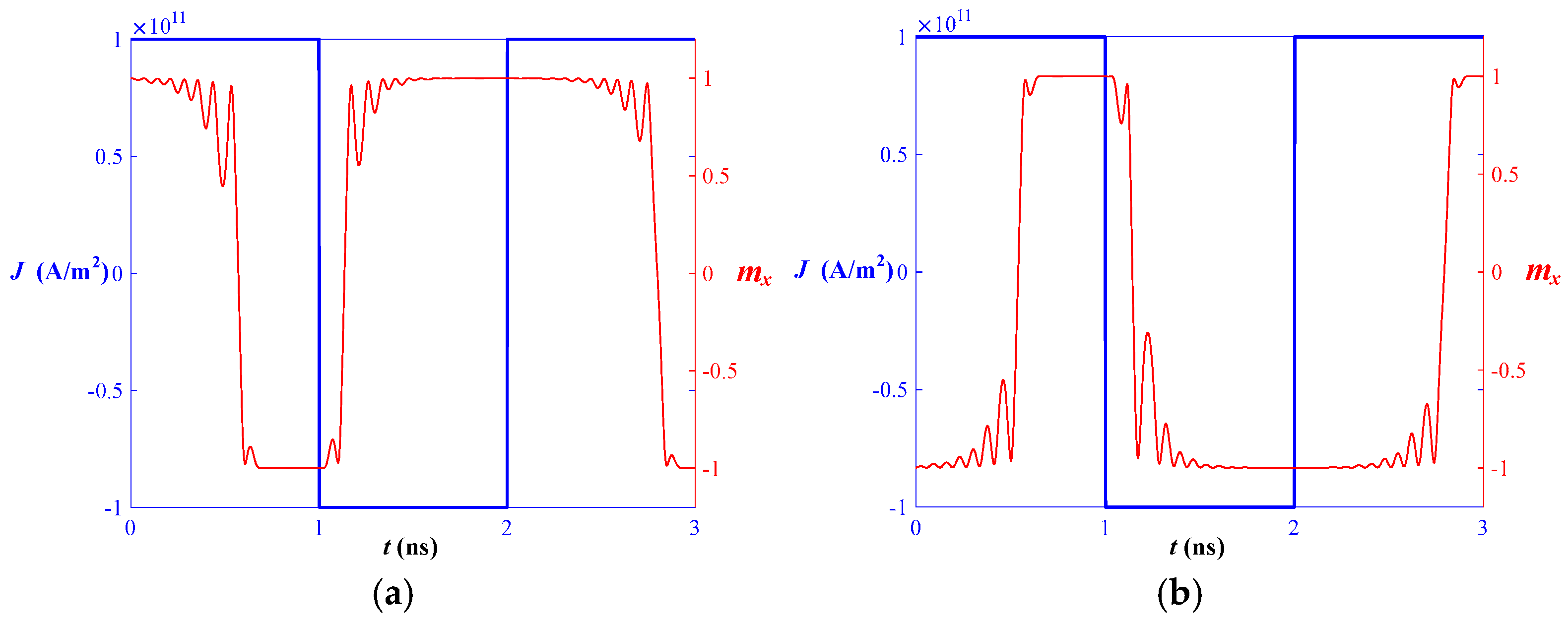
Figure 4 shows the variation of the magnetization of the free layer in the SISF with the polarity of the current density flowing into the MTJ. It can be seen that the magnetization direction of the free layer is opposite to the polarity of the current density when the magnetization direction of the fixed layer points to the +x axis, while the magnetization direction of the free layer is the same as the polarity of the current density when the magnetization direction of the fixed layer points to the −x axis. Based on this, an original or a reverse variable can be input by setting the initial magnetization direction of the fixed layer. Specifically, when the magnetization direction of the fixed layer is set to the +x axis, the inverse variable is input, and when the magnetization direction of the fixed layer is set to the −x axis, the original variable is input.
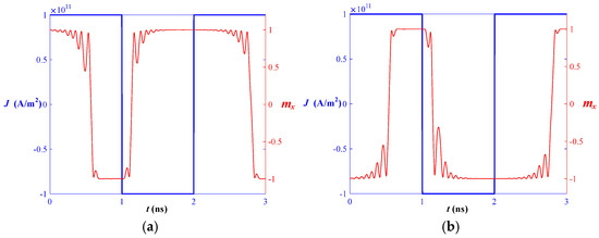
Figure 4.
The magnetization of the free layer varies with the polarity of the current density. From (a) to (b), the magnetization of the fixed layer is in the +x-axis and −x-axis directions, respectively.
According to Equation (3), the inputs of the original variable and the inverse variable are necessary for the decoder. The general practice is to use inverters to transform original variables into inverse variables, as shown in Figure 2. However, according to the above, it is possible to implement the inputs of the original and inverse variables by initializing the MTJ fixed layer in different directions, which eliminates the use of an inverter, thus reducing the signal transmission path and shortening the clock cycle.
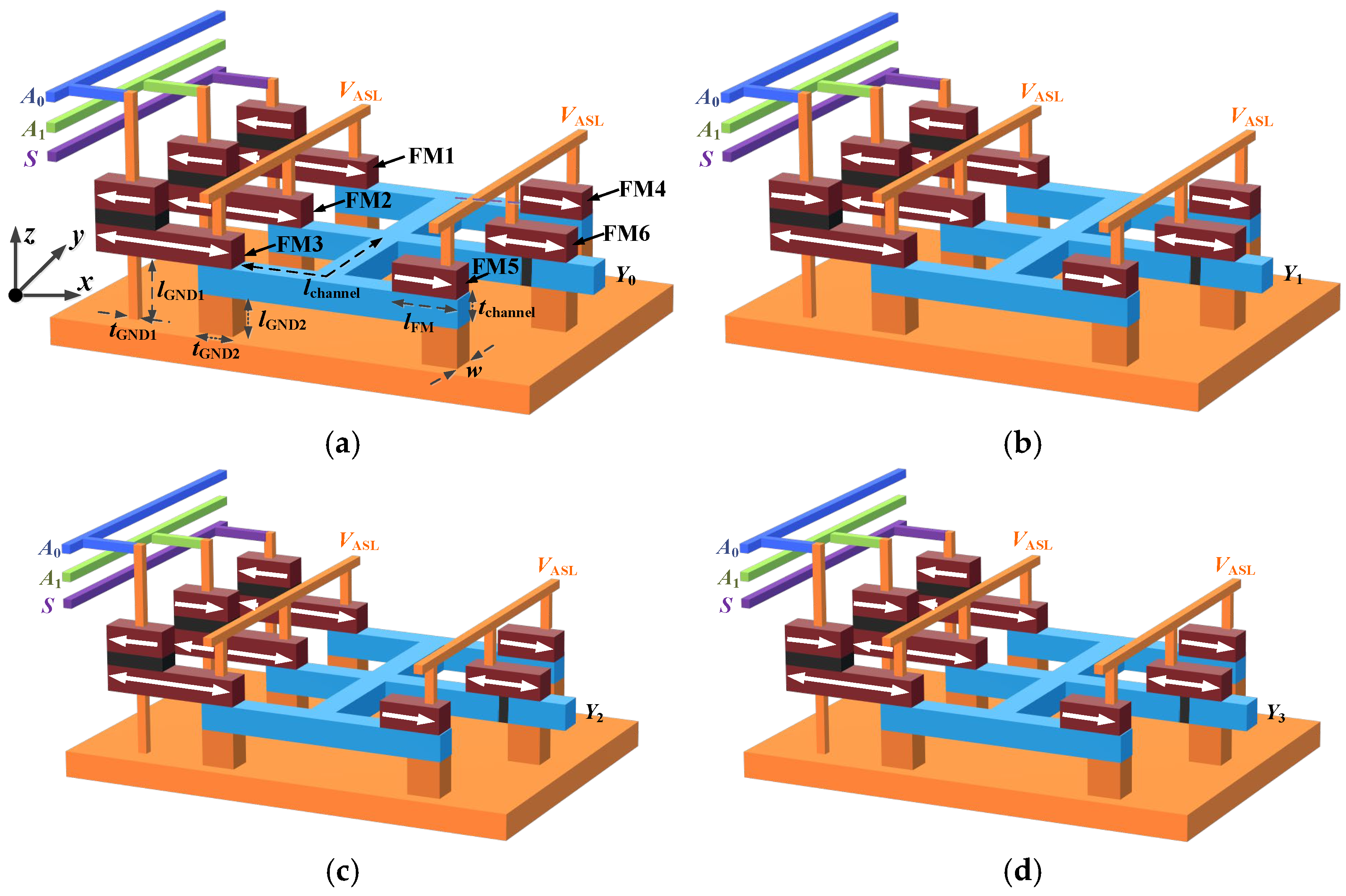
Based on the above description, Figure 5 shows the local layouts of Y0 to Y3, where each local layout is a 5-input minority gate with an SISM structure. FM1, FM2, and FM3 are both the free layers of the MTJ and the inputs of the 5-input minority gate. Their magnetization directions are determined by the input signals S, A1, and A0, respectively. FM4 and FM5 are the inputs of the minority gate, and their magnetizations are fixed to the +x axis direction, representing input logic 1. FM6 is the output of the minority gate, and its magnetization direction is determined by the magnetization direction of the five inputs. When a positive voltage VASL is applied, the 3-input NOR logic function shown in Equation (2) can be realized.
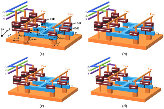
Figure 5.
The local layout of Y0 to Y3: (a) the magnetizations of all three MTJ fixed layers are initialized to the −x axis; (b) the magnetizations of the fixed layers connected to the S and A1 point to the −x axis, while the magnetization of the fixed layer connected to the A0 points to the +x axis; (c) the magnetizations of the fixed layers connected to the S and A0 point to the −x axis, and the magnetization of the fixed layer connected to the A1 points to the +x axis; (d) the magnetization of the fixed layer connected to the S points to the −x axis direction, while the magnetizations of the fixed layers connected to the A0 and A1 point to the +x axis.
It should be noted that although all four local layouts are structurally the same, the magnetization direction of the fixed layer is different in each local layout. If the input is an original variable, the magnetization of the fixed layer connected to that input is initialized to the −x axis direction, and if the input is an inverse variable, the magnetization of the fixed layer is initialized to the +x axis direction.
The four local layouts shown in Figure 5 are connected together to form a complete 2–4 decoder, as shown in Figure 6.
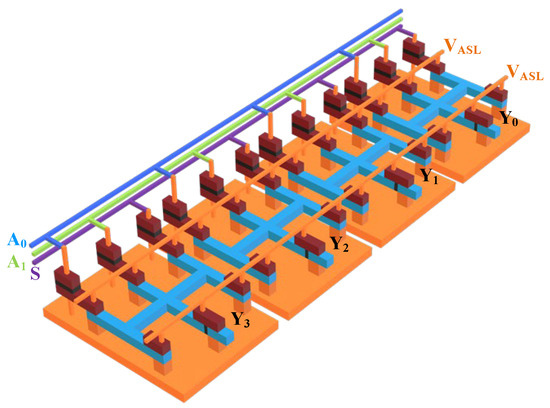
Figure 6.
The overall layout of the 2–4 decoder.
3. Functional Verification of the 2–4 Decoder
The proposed 2–4 decoder consists of four identical 5-input minority gates, and in each minority gate, the magnetizations of FM1~FM3 are affected by the current flowing through the MTJ and the operating voltage VASL, and their magnetization dynamic behavior can be described as follows [29]:
where γ, μ0, α, q, and Ns represent the electron gyromagnetic ratio, the free space permeability, the Gilbert damping of the magnetic material, the magnitude of the electron charge, and the number of Bohr magnetons of FMs, respectively; and are the normalized magnetization of the nth MTJ free-layer and fixed-layer magnets, respectively; and is the spin current flowing into the nth FM. is the effective magnetic field of FM, and is the asymmetric Slonczewski type torque coefficient [19,29].
FM4~FM6 are only affected by the spin current in channels, and their magnetization dynamic behavior can be described as follows [30]:
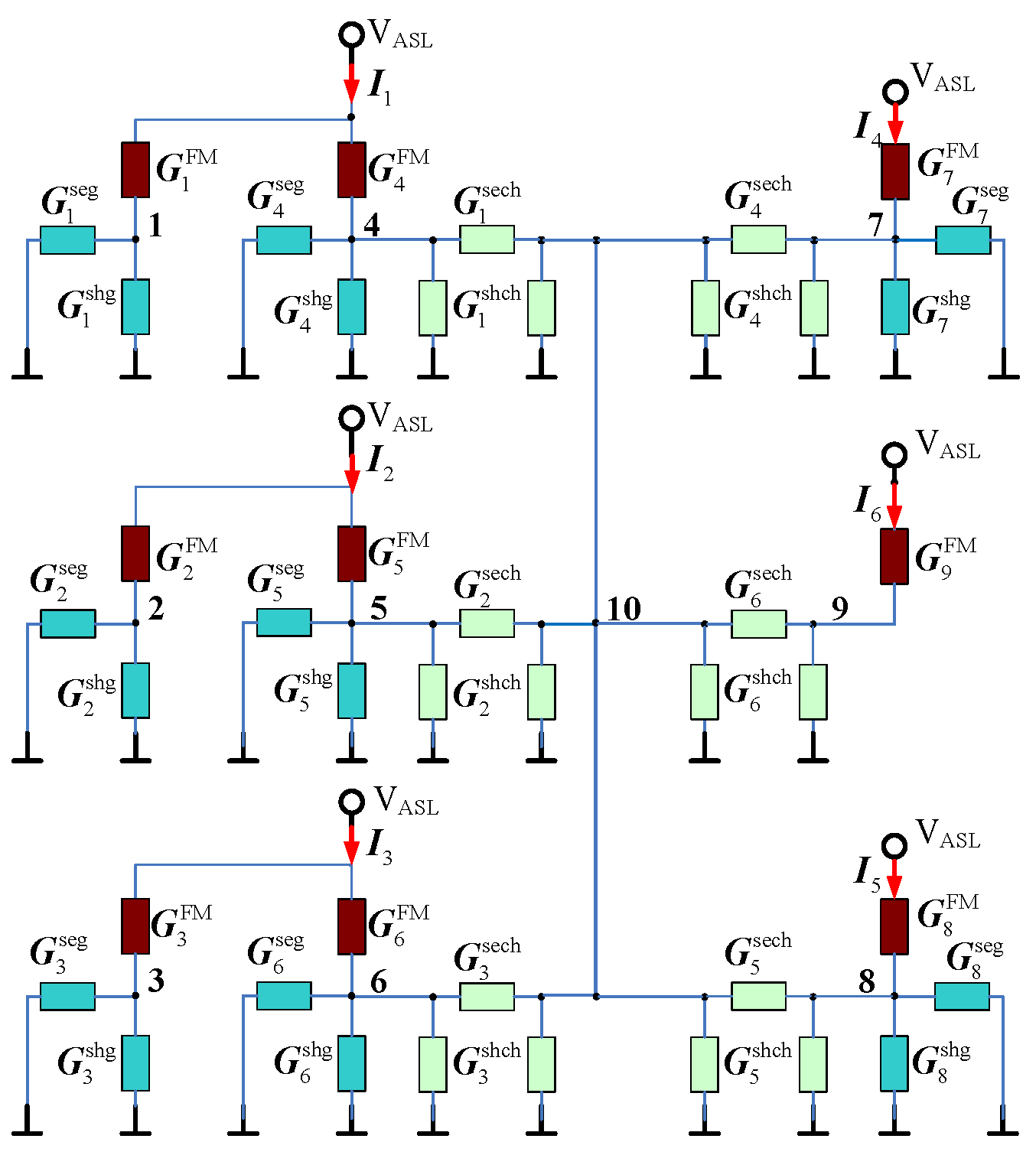
From Equations (4) and (5), it can be seen that to obtain the magnetization precession trajectory of the FMs, it is also necessary to know the spin current . This requires a spin transport model [30] to obtain the spin currents. The equivalent spin transport model for the 5-input minority gate is constructed as shown in Figure 7. is the interface conductance matrix of the interface, and are the series conductance matrix and shunt conductance matrix of the GNDs, and and are the series conductance matrix and shunt conductance matrix of channels [17].

Figure 7.
The equivalent spin transport model for 5-input minority gate.
The voltage vector of each node in Figure 7 can be obtained by a node analysis. And the currents flowing into the FMs can be obtained by the voltage vectors. With the obtained currents, the magnetizations of the FMs are obtained by Equations (4) and (5). By iteratively solving the spin transport model and the magnetization dynamics model, which is usually called the magnetization dynamics/spin transport simulation framework [25,30], the magnetization precession trajectory of the FMs can be obtained.
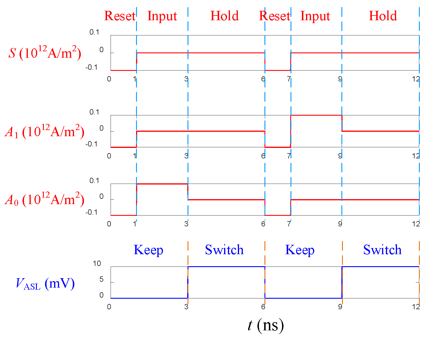
To make the 2–4 decoder work properly, an asynchronous clock control scheme is proposed, as shown in Figure 8, where the input signals are divided into three phases, called “Reset”, “Input”, and “Hold”, and the operating voltage is divided into two phases, called “Keep” and “Switch”. One clock cycle is assumed to be 6ns. It is important to note that the assumed clock period is merely a conservative estimate based on the parameters listed in Table 2, ensuring the decoder’s normal operation. By optimizing the magnet’s size or material [17], or opting for materials with long spin diffusion lengths, such as grapheme, as the channel [16], the clock period can be further shortened.
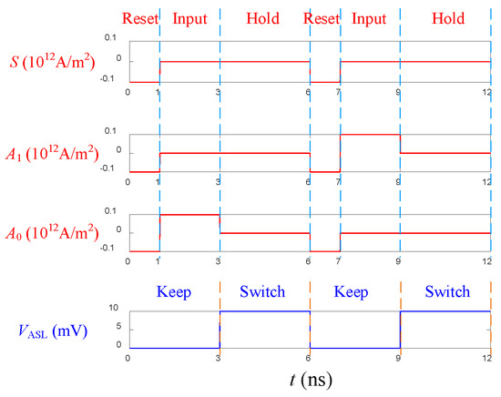
Figure 8.
The asynchronous clock control scheme for the 2–4 decoder.
Table 2.
Default dimension and material parameters for 2–4 decoder.
For the input signal, during the “Reset” phase, the current density is −0.1 × 10¹² A/m2, which causes the magnetization direction of the MTJ free layer to rotate from the initial state to the same direction as that of the MTJ fixed layer, which is called “Reset”.
In the “Input” phase, if the input is a logic “0”, the current density is 0, which causes the magnetization of the free layer to remain constant; if the input is a logic “1”, the current density is 0.1 × 10¹² A/m2, which causes the magnetization direction of the free layer to be opposite to that of the fixed layer.
In the “Hold” phase, the current densities of S, A1, and A0 are all zero, and the magnetizations of FM1, FM2, and FM3 remain unchanged in preparation for the minority gate operation.
For the operating voltage, during the “Keep” phase, the operating voltage VASL applied to the minority gate is 0, the minority gate does not operate, and the magnetization of the FM6 remains unchanged.
In the “Switch” phase, the operating voltage applied to the minority gate becomes 10 mV, and the minority gate starts to operate. The magnetization of FM6 depends on the magnetizations of the five inputs.
In the 2–4 decoder, the parameters of the four 5-input minority gates are completely identical except for the different magnetization directions of the fixed layer. The default parameters are shown in Table 2.
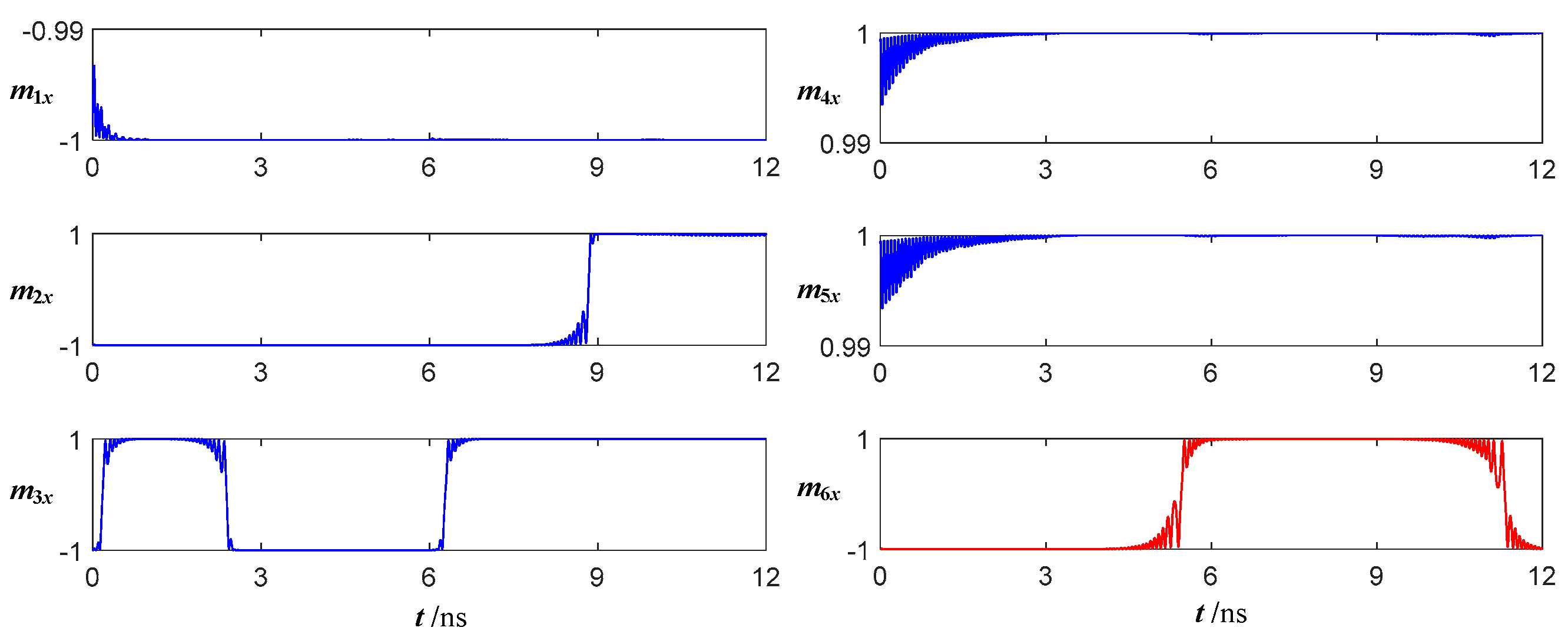
Suppose that the initial magnetization directions of FM4 and FM5 are both + x axis, and the initial magnetization directions of the other FMs are all −x axis. Figure 9 shows the time evolution of magnetization in the x-direction of the 2–4 decoder under the signals shown in Figure 8. Due to space limitations, Figure 9 shows only the time evolution of the x-direction magnetization of six FMs in Y1 (Figure 5b). Assume that when the x-direction magnetization is 1, it means logic 1, and when it is −1, it means logic 0.
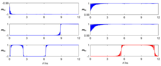
Figure 9.
Simulation result of the Y1.
During 0~1 ns, the input signals are in the “Reset” phase and the magnetization directions of the MTJ fixed layers are as shown in Figure 5b, so m1x and m2x basically remain at −1, while m3x rotates from −1 to +1. At this time, the operating voltage is in the “Keep” phase, the minority gate does not operate, and m4x, m5x, and m6x remain unchanged.
During 1~3 ns, the input signals are in the “Input” phase, the current density of S and A1 is 0, and the current density of A0 is 1 × 10¹¹ A/m2, so that m1x and m2x remain basically unchanged at −1, while m3x rotates from +1 to −1. At this time, the operating voltage is still in the “Keep” phase, and m4x, m5x, and m6x remain unchanged.
During 3~6 ns, the input signals are in the “Hold” phase, so that m1x, m2x, and m3x remain at −1. At this time, the operating voltage is in the “Switch” phase, and the minority gate begins to operate. Since two of the five input FMs’ magnetization directions point to the +x axis, which is a minority, m6x rotates from −1 to +1.
During the period of 6~12 ns, it is the next clock cycle, and the analysis is basically the same as above, so it does not need to be repeated here. In addition, as can be seen in Figure 9, m4x and m5x remain approximately +1 throughout the cycle, indicating that the magnetization directions of FM4 and FM5 always point to the +x axis direction, which is consistent with our expectations.
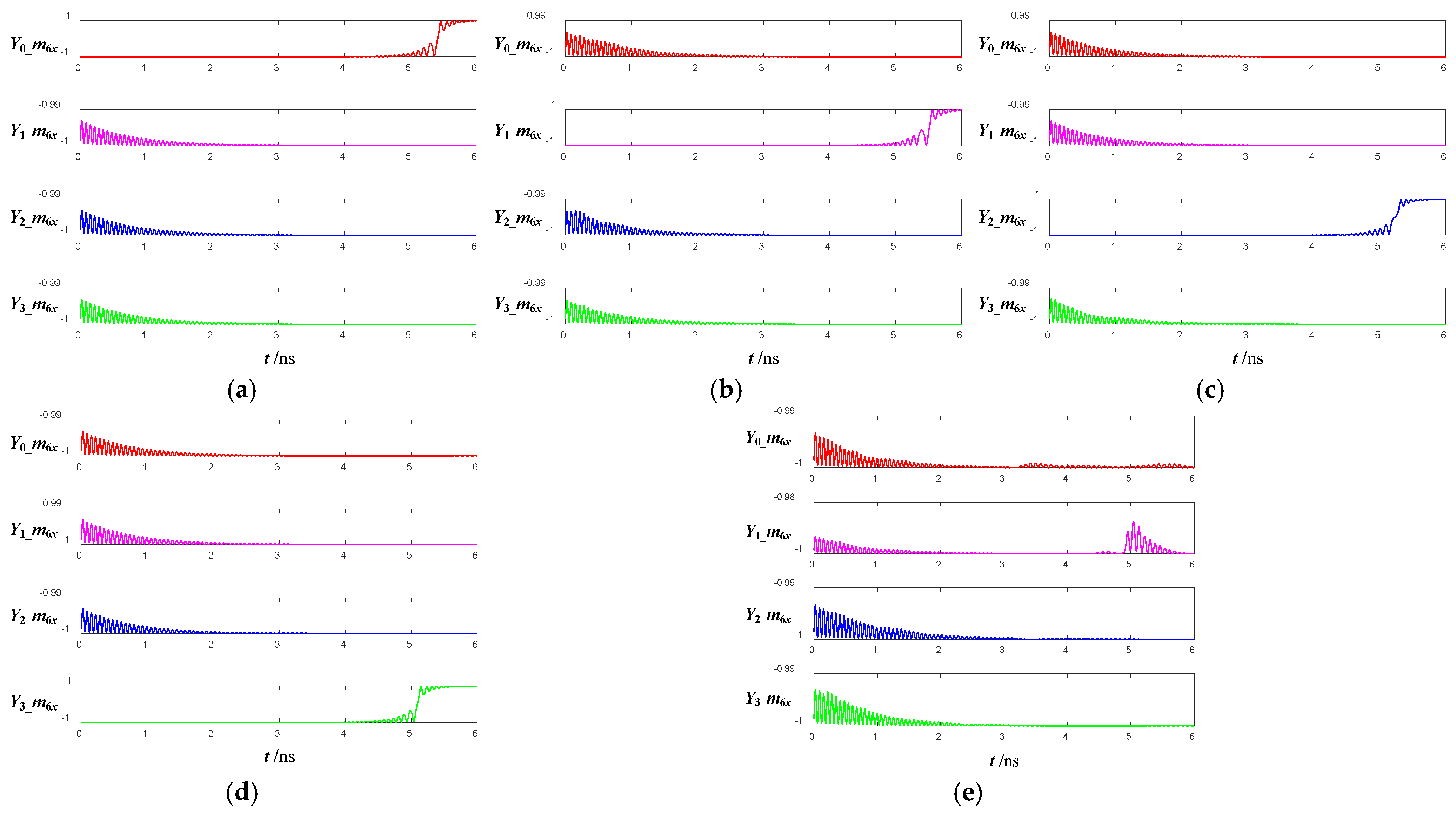
To verify the function of each subcircuit shown in Figure 5, Figure 10 shows the time evolution of the x-direction magnetization of outputs Y0, Y1, Y2, and Y3 under different inputs.
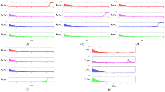
Figure 10.
The 2–4 decoder simulation results for different inputs. During 1~3 ns, the logic value of S, A1, and A0 in (a–d) is 000~011, respectively, and the logic value of S, A1, and A0 in (e) is 110.
From Figure 10a–d, in the “switch” phase, when SA1A0 = 000, Y0Y1Y2Y3 = 1000; when SA1A0 = 000 = 001, Y0Y1Y2Y3 = 0100; when SA1A0 = 000, Y0Y1Y2Y3 = 0010; and when SA1A0 = 000 = 011, Y0Y1Y2Y3 = 0001. Moreover, Figure 10e shows that there is Y0Y1Y2Y3 = 0000 when SA1A0=110. (Due to space limitations, only the simulation results of SA1A0 = 110 are shown. If SA1A0 = 100, SA1A0 = 101, or SA1A0 = 111, there is still Y0Y1Y2Y3 = 0000.) This is entirely consistent with Table 1, which verifies that the 2–4 decoder functions correctly.
4. The Results and Discussions
The total energy dissipation of the 2–4 decoder consists of the energy dissipation of the MTJs and the energy dissipation of the minority gates, as follows:
The energy dissipation of the MTJs is
where T is the clock cycle, is the cross-sectional area of the k-th MTJ, and is the resistance of the k-th MTJ, and can be expressed as
and are the MTJ resistances when the magnetization directions of the fixed layer and the free layer are parallel and anti-parallel, respectively. And θ(t) is the angle between the magnetization vectors of free layer and fixed layer, which varies with time.
The energy dissipation of minority gates is
where is the charge current flowing into the k-th FM in the i-th minority gate.
Table 3 shows the energy dissipation of the MTJs and minority gates under different inputs. It can be seen that the is basically the same under different inputs, which is about 9.30 pJ. This is because the energy dissipation of minority gates is mainly determined by the charge currents flowing into FMs and the operating voltage VASL applied to them, and the charge currents are not affected by the inputs, so different inputs have little effect on the energy dissipation of minority gates. However, the varies greatly under different inputs, because when the input signal changes, the current density flowing into the MTJs changes accordingly, and it can be seen from Equation (8) that the will be different.
Table 3.
The energy dissipation of MTJs and minority gates under different inputs.
The energy dissipation of the MTJ, which is also the energy dissipation of the SISF structure, only has an average value of about 0.23 pJ, which is about 1/40 of the energy dissipation of the MTJs and minority gate. This shows that the increase in the energy dissipation of the MTJs due to the increase in the number of MTJs resulting from the employment of the SISF structure is negligible.
In addition, according to the research findings presented in Refs. [31,32], replacing the insulating layer in the MTJ with Sr2RuO4, an unconventional superconducting material, could potentially eliminate the charge current and only retain the spin current within the MTJ, thereby further reducing its energy consumption. Consequently, the marginal increase in energy consumption resulting from an increase in the number of SISFs will become even more negligible.
To illustrate the advantages of the five-input minority gate and SISF structure in designing the 2–4 decoder, another 2–4 decoder designed using three-input minority gates, inverters, and a single-input multi-fan-out (SIMF) structure is given below and is called the second decoder for convenience. The logical expression for the second decoder is
where denotes a three-input minority gate, and when one of the inputs is set to 1, its logical expression becomes
According to Equation (11), the 2D schematic diagram of the second decoder is shown in Figure 11. To avoid the crossover of channels, the three inputs are not in the same plane. The channel connected to A1 is in the top layer, A0 is in the middle layer, and S is in the bottom layer. The white arrow indicates that the input FM of the three-input minority gate is magnetized in the +x-axis direction, representing logic 1.
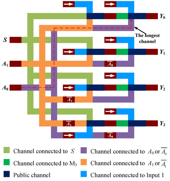
Figure 11.
The 2D schematic diagram of the second decoder.
Table 4 shows the performance comparison of the two types of 2–4 decoders. The dimensional parameters in Table 2 are used for both decoders, and in addition, the spacing between each minority gate is assumed to be 20 nm. Compared to the second decoder, the first decoder (decoder shown in Figure 5) reduces the total channel length to 40.8%, the layout area to 37.9%, and the number of clock cycles to one-third. In particular, the second decoder has a maximum channel length of 1430 nm, which exceeds the spin diffusion length of most currently known metallic materials, which would cause the decoder to fail. Therefore, the simulation results for the operation of the second decoder are not provided here. In addition, despite the increase in the number of FMs in the first decoder, mainly by nine MTJs, its impact on energy dissipation is negligible according to the previous description.
Table 4.
Performance comparison of the two decoders.
In summary, for logic circuits such as 2–4 decoders with multiple identical inputs, the use of the SISF structure and multiple-input minority gates can result in significant improvements in terms of layout area, clock cycles, and so on.
5. Conclusions
In this paper, a 2–4 decoder based on ASL and a MTJ is proposed, and its logic function is verified by a magnetization dynamics/spin transport self-consistent simulation framework. The proposed 2–4 decoder employs an SISF structure to provide input to the circuit, thus reducing the channel length of the circuit. At the same time, five-input minority gates are employed, which greatly simplifies the circuit scale. In addition, the original variables and the inverse variables are realized by setting the magnetization of the MTJ fixed layer in different directions, which avoids the use of inverters and further reduces the circuit scale. Compared to the 2–4 decoder using three-input minority gates, inverters, and the SIMF structure, the proposed 2–4 decoder shows significant improvement in maximum channel length, total channel length, layout area, and the number of clock cycles, except for the number of FMs. Most importantly, the design methods used in this paper, such as the SISF structure, multi-input majority/minority gate, and inverter-free structure, provide a way to design more large-scale ASL circuits in the future.
Author Contributions
Design, S.W.; Functional Verification, S.W. and Y.Z.; Writing, S.W.; Visualization, Y.Z. and D.S. All authors have read and agreed to the published version of the manuscript.
Funding
This research was funded by the Basic Research Program of the Liaoning Education Department, grant number JYTMS20231868.
Data Availability Statement
The data that support the findings of this study are available from the corresponding author upon reasonable request.
Conflicts of Interest
The authors declare no conflicts of interest.
References
- Rajput, P.J.; Bhandari, S.U.; Wadhwa, G. A review on—Spintronics an emerging technology. Silicon 2022, 14, 9195–9210. [Google Scholar] [CrossRef]
- Yakout, S.M. Spintronics: Future technology for new data storage and communication devices. J. Supercond. Nov. Magn. 2020, 33, 2557–2580. [Google Scholar] [CrossRef]
- Hu, G.; Xiang, B. Recent advances in two-dimensional spintronics. Nanoscale Res. Lett. 2020, 15, 226. [Google Scholar] [CrossRef]
- Liu, Y.; Zeng, C.; Zhong, J.; Ding, J.; Wang, Z.M.; Liu, Z. Spintronics in two-dimensional materials. Nano-Micro Lett. 2020, 12, 93. [Google Scholar] [CrossRef] [PubMed]
- Dattagupta, S. Two-dimensional spintronics in a magnetic field—An overview of salient theory. Pramana—J. Phys. 2022, 96, 23. [Google Scholar] [CrossRef]
- Hirohata, A.; Yamada, K.; Nakatani, Y.; Prejbeanu, I.L.; Diény, B.; Pirro, P.; Hillebrands, B. Review on spintronics: Principles and device applications. J. Magn. Magn. Mater. 2020, 509, 166711. [Google Scholar] [CrossRef]
- Barla, P.; Joshi, V.K.; Bhat, S. Spintronic devices: A promising alternative to CMOS devices. J. Comput. Electron. 2021, 20, 805–837. [Google Scholar] [CrossRef]
- Sugahara, S.; Tanaka, M. A spin metal–oxide–semiconductor field effect transistor using half-metallic-ferromagnet contacts for the source and drain. Appl. Phys. Lett. 2004, 84, 2307–2309. [Google Scholar] [CrossRef]
- Cowburn, R.P.; Welland, M.E. Room temperature magnetic quantum cellular automata. Science 2000, 287, 1466–1468. [Google Scholar] [CrossRef] [PubMed]
- Allwood, D.A.; Xiong, G.; Faulkner, C.C.; Atkinson, D.; Petit, D.; Cowburn, R.P. Magnetic domain-wall logic. Science 2005, 309, 1688–1692. [Google Scholar] [CrossRef]
- Behin-Aein, B.; Datta, D.; Salahuddin, S.; Datta, S. Proposal for an all-spin logic device with built-in memory. Nat. Nanotechnol. 2010, 5, 266–270. [Google Scholar] [CrossRef] [PubMed]
- Khitun, A.; Wang, K.L. Nano scale computational architectures with spin wave bus. Superlatt. Microstruct. 2005, 38, 184–200. [Google Scholar] [CrossRef]
- Nikonov, D.E.; Bourianoff, G.I. Spin gain transistor in ferromagnetic semiconductors: The semiconductor Bloch equations approach. IEEE Trans. Nanotechnol. 2005, 4, 206–214. [Google Scholar] [CrossRef]
- Chang, S.C.; Kani, N.; Manipatruni, S.; Nikonov, D.E.; Young, I.A.; Naeemil, A. Scaling limits on all-spin logic. IEEE Trans. Magn. 2016, 52, 3400404. [Google Scholar] [CrossRef]
- Su, L.; Zhao, W.S.; Zhang, Y.; Querlioz, D.; Zhang, Y.G.; Klein, J.O.; Dollfus, P.; Bournel, A. Proposal for a grapheme-based all-spin logic gate. Appl. Phys. Lett. 2015, 106, 072407. [Google Scholar] [CrossRef]
- Zhang, Z.Z.; Zhang, Y.; Zheng, Z.Y.; Wang, G.D.; Su, L.; Zhang, Y.G.; Zhao, W.S. Energy consumption analysis of graphene based all spin logic device with voltage controlled magnetic anisotropy. AIP Adv. 2017, 7, 055925. [Google Scholar] [CrossRef]
- Wang, S.; Cai, L.; Qi, K.; Yang, X.K.; Feng, C.W.; Cui, H.Q. Impact of nanomagnets size on switching behavior of all spin logic devices. Micro Nano Lett. 2016, 11, 508–513. [Google Scholar] [CrossRef]
- Manipatruni, S.; Nikonov, D.E.; Young, I.A. Material targets for scaling all-spin logic. Phys. Rev. Appl. 2016, 5, 014002. [Google Scholar] [CrossRef]
- Zhang, Y.; Zhang, Z.Z.; Wang, L.Z.; Nan, J.; Zheng, Z.Y.; Li, X.; Wong, K.; Wang, Y.; Klein, J.O.; Amiri, P.K.; et al. Partial spin absorption induced magnetization switching and its voltage-assisted improvement in an asymmetrical all spin logic device at the mesoscopic scale. Appl. Phys. Lett. 2017, 111, 052407. [Google Scholar] [CrossRef]
- Iraei, R.M.; Kani, N.; Dutta, S.; Nikonov, D.E.; Manipatruni, S.; Young, I.A.; Heron, J.T.; Naeemi, A. Clocked magnetostriction-assisted spintronic device design and simulation. IEEE Trans. Electron. Devices 2018, 65, 2040–2046. [Google Scholar] [CrossRef]
- Gao, T.Q.; Zeng, L.; Zhang, D.M.; Qin, X.W.; Long, M.Z.; Zhang, Y.; Lin, X.Y.; Zhang, Y.G.; Zhao, W.S. Negative capacitance enhanced all spin logic devices with an ultra-low 1 mV working voltage. IEEE J. Electron. Devices 2018, 6, 245–249. [Google Scholar] [CrossRef]
- Hassan, N.; Saha, D.; Linseisen, C.M.; Vyas, V.; Friedman, J.S. Energy efficiency challenges for all-spin logic. Microelectron. J. 2021, 110, 105008. [Google Scholar] [CrossRef]
- Patra, M.; Maiti, S.K. All-spin logic operations: Memory device and reconfigurable computing. Europhys. Lett. 2018, 121, 38004. [Google Scholar] [CrossRef]
- An, Q.; Beux, S.L.; O’Connor, I.; Klein, J.O. A comprehensive compact model for the design of all-spin-logic based circuits. Microelectron. J. 2019, 92, 104442.1–104442.10. [Google Scholar] [CrossRef]
- Calayir, V.; Nikonov, D.E.; Manipatruni, S.; Young, I.A. Static and clocked spintronic circuit design and simulation with performance analysis relative to CMOS. IEEE Trans. Circuits Syst. I 2014, 61, 393–406. [Google Scholar] [CrossRef]
- Augustine, C.; Panagopoulos, G.; Behin-Aein, B.; Srinivasan, S.; Sarkar, A.; Roy, K. Low-power functionality enhanced computation architecture using spin-based devices. In Proceedings of the 2011 IEEE/ACM International Symposium on Nanoscale Architectures, San Diego, CA, USA, 8–9 June 2011. [Google Scholar] [CrossRef]
- Wang, S.; Cai, L.; Feng, C.W.; Cui, H.Q.; Yang, X.K.; Zhao, H.Y. RS flip-flop implementation based on all spin logic devices. Micro Nano Lett. 2017, 12, 396–400. [Google Scholar] [CrossRef]
- Wang, S.; Yang, Y.; Song, W.B.; Cui, H.Q.; Li, C.; Cai, L. All-spin logic XOR gate implementation based on input interface. IET Circuits Device Syst. 2019, 13, 607–613. [Google Scholar] [CrossRef]
- Wang, S.; Zhang, Y.F.; Wang, X.Y.; Cong, G.T.; Zhang, X.X. Proposal for an input interface and multi output structures of all-spin logic circuits based on magnetic tunnel junction. IET Circuits Device Syst. 2020, 14, 838–845. [Google Scholar] [CrossRef]
- Manipatruni, S.; Nikonov, D.E.; Young, I.A. Modeling and design of spintronic integrated circuits. IEEE Trans. Circuits Syst. I Reg. Pap. 2012, 59, 2801–2814. [Google Scholar] [CrossRef]
- Kuboki, K.; Takahashi, H. Spontaneous spin current near the interface between unconventional superconductors and ferromagnets. Phys. Rev. B 2004, 70, 214524. [Google Scholar] [CrossRef]
- Kuboki, K.; Yano, K. Microscopic Derivation of Ginzburg–Landau Equations for Coexistent States of Superconductivity and Magnetism. J. Phys. Soc. Jpn. 2012, 81, 064711. [Google Scholar] [CrossRef]


Disclaimer/Publisher’s Note: The statements, opinions and data contained in all publications are solely those of the individual author(s) and contributor(s) and not of MDPI and/or the editor(s). MDPI and/or the editor(s) disclaim responsibility for any injury to people or property resulting from any ideas, methods, instructions or products referred to in the content. |
© 2025 by the authors. Licensee MDPI, Basel, Switzerland. This article is an open access article distributed under the terms and conditions of the Creative Commons Attribution (CC BY) license (https://creativecommons.org/licenses/by/4.0/).