Article

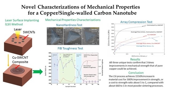
Novel Characterizations of Mechanical Properties for a Copper/Single-Walled Carbon Nanotube Nanocomposite Synthesized by Laser Surface Implanting

1
Department of Mechanical and Aerospace Engineering, North Carolina State University, Raleigh, NC 27695-8501, USA
2
Independent Consultant, Bengaluru 560002, Karnataka, India
3
Division of Mechanical Design Engineering, Jeonbuk National University, 664-14, Duckjin-dong, Duckjin-gu, Jeonju, Seoul 561-756, Korea
*
Author to whom correspondence should be addressed.
Submission received: 24 January 2020 / Revised: 14 February 2020 / Accepted: 25 February 2020 / Published: 29 February 2020
(This article belongs to the Special Issue Surface Modification of Carbons)

Abstract

:
In our previous studies, we have developed a wet process, denoted laser surface implanting (LSI), to synthesize a copper/single-walled carbon nanotube (Cu–SWCNT) metal nanocomposite as an implant onto the surface of a pure copper substrate. The nanostructure of this Cu–SWCNT composite was confirmed independently by several methods, including transmission electron microscope (TEM) images, which show discernable SWCNT clusters in nano sizes inside the copper matrix. The hardness was measured by micro-hardness tests to indicate over three times hardness over that of pure copper could be achieved. In this paper, we present several unique ways to further characterize the mechanical properties of the Cu-SWCNT nanocomposite. Nano-hardness tests are first performed to confirm that hardness improvement, about three times that of pure copper, is achieved, consistent with the micro-hardness test results. A new toughness measurement based on focus ion beam (FIB) bombardment was performed to demonstrate 2.5 times toughness improvement. Finally, a new compression test rig was designed to conduct plane strain compression test for an array of Cu-SWCNT implants. The results confirmed that the Cu-SWCNT nanocomposite exhibits a stress-strain behavior consistent with the results of the hardness and FIB tests.

Graphical Abstract

1. Introduction

Carbon nanotubes (CNTs), due to their exceptional structural properties, are ideal reinforcing elements to form composites for structural applications [1,2,3]. CNT-reinforced composite research first focused on polymer composites, and subsequently, metal composites. One major challenge in the synthesis of CNT–metal composites is the difficulty to achieve uniform dispersion of CNTs at small cluster sizes. This challenge is a result of CNTs’ tremendous surface area, up to 200 m2/g, for which van der Waals forces can lead to the formation of large clusters. Summaries and applications of metal–CNT composites can be found in several reviews, and one successful example is CNT-reinforced aluminum for high-frequency MEMS (Mechanical-Electrical Micro-Systems) resonators [4,5,6].
Copper is one of the most important industrial materials due to its excellent thermal and electric conductivities. However, copper is a soft material with poor wear resistance. Although copper alloys can offer higher strength over pure copper, they suffer substantial reductions in both thermal and electric conductivities. If copper could be strengthened without significant loss of these two properties, it could become an ideal material for many critical applications. In order to retain the thermal and electric properties of copper, the enforcement element for a copper composite must have better or equal thermal and electric conductivities than those of copper. One element which qualifies for this requirement is carbon nanotubes.
However, the synthesis of Cu–CNT composites is considered, in general, more difficult than Al–CNT composites because copper and carbon do not form intermetallic compounds, as in the case of aluminum and carbon, which form aluminum carbide. In addition, copper and carbon are not soluble. As a result, most Cu-CNT synthesis processes, reported in the literature, utilize powder metallurgy and sintering. A detailed review of this powder metallurgy-based process can be found in [7,8]. These powder-based processes are denoted as the dry process in this paper. The strength improvement using the dry process typically is less than 200% with 15–20% CNT volume fraction. The key obstacle is that, due to CNTs’ tremendous surface area to result in large van der Waals forces; as aresult, it is very difficult to break up CNT into sub-micron clusters, despite long hours of mixing by ball end mills [8].

1.1. Wet Synthesis of Cu–SWCNT Nanocomposite

A wet process, denoted as laser surface implanting (LSI), was reported in [7,8] for the synthesis of copper–single-walled carbon nanotube (Cu–SWCNT) nanocomposites. This process disperses single-walled carbon nanotube (SWCNTs) into molten copper, followed by rapid and non-equilibrium solidification to lock SWCNTs in positions without agglomerating into large clusters.
This wet process is different from the typical dry powder metallurgy method, commonly reported in the literature. Rapid and non-equilibrium solidification is achieved when the heat of the molten copper is rapidly conducted away into the copper substrate due to copper’s excellent heat conductivity.
As shown in Figure 1, described in details in [8], this novel synthesis process includes: Step (1): A 300 W single-mode fiber laser beam is focused to a 10 µm spot size to drill a number of microholes (17 µm in diameter and depth) arranged around a circle of 70 µm diameter (Figure 1a); Step (2): The microholes are filled with SWCNTs suspended in solution; Step (3): The same laser beam with the same spot size of 10 µm is used to irradiate at the center of the above microhole circle to create a well of molten copper. The molten copper advances radially outward to engulf the microholes with pre-deposited SWCNTs (Figure 1b) to form the Cu-SWCNT implant upon rapid and non-equilibrium solidification (Figure 1c). Rapid and non-equilibrium solidification is achieved due to copper’s excellent heat conductivity so that SWCNTs are locked in positions within copper matrix without agglomerating into large clusters. Detailed process parameters of LSI are presented in [8].
The nanostructure of the Cu–SWCNT composite is confirmed independently by energy-dispersive X-ray spectroscopy mapping, spectroscopy measurements, and TEM images with discernable SWCNT clusters in the nano-dimension, as shown in Figure 2c. Many detailed TEM images of the Cu-SWCNT with their refraction index patterns were presented in [9].
However, TEM images with discernable nano-sized SWCNT clusters are rare, the analysis of indirect TEM image patterns, such as moiré fringes, to infer the existence of SWCNT clusters within the copper matrix was presented in [10]. Moiré fringes or patterns in the TEM images of a Cu–SWCNT nanocomposite could be generated due to the overlapping of two or more thin crystals with similar periodic arrangements of atoms, promoted by SWCNT clusters. However, the presence of moiré patterns is not a sufficient or a necessary condition for the existence of SWCNT clusters. It was found that based on the overlapping angle of two periodic arrangements, it is feasible to distinguish the moiré fringes induced by SWCNT clusters from those by other factors, such as dislocations. The ability to identify SWCNTs within the copper matrix based on indirect TEM moiré patterns helps to widen the usability of TEM images.
The readers should refer to [8,9,10] for comprehensive review of the LSI process versus the dry process, as well as the nano-structure of the Cu-SWCNT nanocomposite synthesized by the LSI process.

1.2. Vickers Micro-Hardness Tests

Micro-harness test results for the Cu-SWCNT nanocomposite synthesized by the LSI were reported in [7,8]. A Tukon micro-hardness tester with a Vickers diamond square-based pyramid indenter was used to measure the hardness of Cu-SWCNT nanocomposite at 100 gmf load for ten seconds. The hardness for pure copper was found to be 74 kgf/mm2 (HV 74) (Figure 2a). On the perimeter of the Cu-SWCNT nanocomposite, the average hardness was found to be 464 kgf/mm2 (HV 464). This indicates it is 627% that of pure copper. It should be noted that typical H13 steel has a hardness of HV 372−412. These results are very consistent across several samples tested.
While the hardness measurements are consistent at the perimeter of the implant, the hardness measurements near the center show substantial variations. In some samples, a hardness of 210 kgf/mm2 (HV 210) was found, as shown in Figure 2b. This hardness value is less than the hardness measured at the perimeter; however, it still represents 285% that of pure copper, harder than the hardest brass (cold rolled, HV 180).
Although the micro-hardness test indicates excellent strength improvement, the results are not independently confirmed by other mechanical property tests, such as the standard tensile test. Due to the small size of the Cu-SWCNT nanocomposite and it being an implant onto a pure copper substrate, the sample is not homogeneous, required by the standard tensile test.
In Section 2, we present several unique methods to characterize the mechanical properties of the Cu-SWCNT nanocomposite. These methods include nano-indentation tests, focus ion beam bombardment tests, and plane strain compression tests.

2. Method and Results

2.1. Berkovich Nanoindentation Tests

In nano-indentation, as its name suggests, very small indentations are made on the surface with penetration depths ranging in the nanometer scale. The Berkovich indenter, which is designed to give the same area-to-depth ratio as the Vickers indenter, is most commonly used in this test. Since the calculation of actual contact area is very difficult to predict with this technique, the hardness of the material is calculated as Meyer hardness, which is based on a projected area instead of actual contact area [11]. For the Cu-SWCNT implant, due to its uneven surface profile, this projected area suffer from poor accuracy; therefore, the corresponding hardness measurement became unusable. To remedy this problem, SEM was used to determine the actual indentation area for hardness calculation.
Nano-indentation tests were performed using Hysitron Ubi-1 Triboindenter (Bruker Nano Surface Offices, Billerica, MA, USA) with the Berkovich indenter. During initial studies, a maximum load of 9000 µN was applied to the specimen. The loading and unloading rate of 250 µm/s was selected with a hold time of 10 s after maximum load had reached. Due to the limitations of the microscope on the indenter, it was difficult to choose the exact site of the indentation on the implant. As a result, the indenter was programmed to perform many indentations over a large area that contains the Cu-SWCNT implant. The entire indentation process could take several hours to complete. The sample was then examined by SEM to find valid indentation marks for hardness calculation.
Figure 3 shows some images of indentations from this test. Due to the uneven surface of the implant, it was difficult to get the signature triangular marks of the Berkovich indenter. It was found that implant surface at the middle region had a hardness of 1992 MPa (Figure 3c) which is about 306% that of pure copper of 652 MPa (Figure 3a). At the edge of the implant, the hardness was found to be 1282 MPa (Figure 3b), or 197% that of pure copper. While the center hardness is consistent with the micro-hardness test, the perimeter hardness is substantially lower.
The nano-indentation test was also repeated with a lower maximal load at 7000 µN. It was found that implant surface at the middle region had a hardness of 1972 MPa (Figure 3e), which is about 302% that of pure copper of 652 MPa. At the edge of the implant, the hardness was found to be 1663 MPa (Figure 3d), or 255% that of pure copper.
The hardness of a material is related to its yielding and ultimate strengths. However, the hardness measurement does not provide information regarding the toughness, ductility, and stress-strain curve of the material. A new method is presented in the next section to measure the toughness. The toughness of a material is the energy per unit volume a material can absorb before fracturing.

2.2. Toughness Test

A toughness characterization study of a nanocomposite implant was carried out using a focused ion beam (FIB) machine (FEI Quanta 3D FEG, ThermoFisher Scientific, Hillsboro, OR, USA). FIB is an effective method to process samples for TEM measurements. Detailed sample preparation for TEM imaging to obtain samples with a thickness about 40 nm and extremely smooth surface roughness can be found in [9].
The operation principle of the FIB is that energized ions, with programmed kinetic energy, are used to bombard the sample. Upon hitting the sample by an ion, a small amount of the material was removed. The material is removed because it absorbs the energy of the ion that exceeds the toughness of the material.
As a result, it can be assumed that if the kinetic energy of the bombardment ion is kept constant and the material is bombarded for a fixed amount of time, then the material removal will depend upon the toughness of the material.

2.2.1. Ion Bombardment Results

Before the FIB bombardment test could be performed, FIB was first used to cut into the Cu-SWCNT implant to expose its cross-section, as shown in Figure 4. This process can take over 10 hours to complete. As shown in Figure 4, the top surface of the implant can be seen in the back ground with similar bulging perimeter as shown in Figure 1c. The cross-section cut down is about 90 μm wide and a depth about 20 μm. The cross-section surface was then further polished by FIB to render it smooth.
The ion beam was then programed to bombard the smooth cross-section to form rectangular craters. Sixteen craters were produced at 16 different locations, covering different regions of the sample. Typical sizes of these rectangular craters are approximately 2 μm × 10 μm.
As shown in Figure 4, two craters (craters #1–#2) were produced in the region of pure copper, not irradiated by the laser. Seven craters (craters #3–#9) were produced in the perimeter of implant. Finally, seven more craters (craters #10–#16) were created in the inner region of the implant, where high concentration of SWCNT likely exists, based on Figure 1. The dimensional measurements shown in Figure 4 were generated by the FIB machine. The machine was pre-programmed with five significant digits. However, it should be noted that, despite the measurements being shown with three digits behind the decimal point (0.001 μm), we rounded these measurement to one digit behind the decimal point in our analysis.
These craters were further examined by SEM. The depth measurements were taken at different locations along their lengths of the rectangular craters. The close-up views of three craters are shown in Figure 5.
The FIB bombardment test also reveals the micro-structure of the material. For example, crater# 1 of Figure 5, is approximately 2 μm wide and 10 μm long and locates in the pure copper region, and it contains three large copper grains inside the rectangular crater. The grain boundaries can be distinguished clearly. The texture of two of these grains on the right is smooth, while the third grain shows a texture with longitudinal stripes. The large grain size is consistent with that of annealed copper substrate. The average depth of crater #1 is 425.7 μm.
Crater #8 in Figure 5 locates outer perimeter of the implant, likely with low concentration of SWCNTs. Crater #8 also contains three grains. However, the surface texture of these grains is not as smooth as that of crafter #1. The copper substrate of crater #8 was melted by the laser and resolidified. The average depth of crater #8 is 390.9 μm, but the depth variation is large.
Crater#16 is significant different from the other two craters of Figure 5. First, the average depth is 174.3 μm, substantially lower than those of craters #1 and #8. It also demonstrates a very different texture. It is difficult to identify any grain boundaries in this crater. The texture itself might indicate small grain sizes. Crater #16 locates in the region where high SWCNT concentration likely exists. It is conceivable that the fine texture and much shallower depth of crater #16 are due to the existence and the strengthening effect of SWCNTs.
In the next section, we propose a model to correlate the crater depth to the material property of each crater of Figure 4.

2.2.2. Ion Bombardment Model

As discussed above, when the FIB machine blasts an ion onto the sample, the ion removes the material by impact and energy absorption, similar to bombing. The toughness of the material is the energy absorbed by the material before fracturing. With respect to the stress-strain curve of a material obtained in a standard tensile test, the toughness is the area under the stress-strain curve before fracture. Therefore, it is expected, for the same ion energy, more material would be removed for a material with a lower toughness.
Let T i be the toughness of material i, and we define the energy, E 0 , deposited by the ion beam as
E 0 = P 0   Δ t = T i   A 0   d i  
where P 0 is the programmed power of the ion beam, Δ t is the time of the ion bombardment, A 0 is the area of the rectangular crater, and d i is the depth of the crater, observed in Figure 4 and Figure 5.
With the scanning rate of FIB specified by the operator as   S 0 , we have
A 0 = S 0   Δ t  
The expression for the toughness, T i , becomes
T i = P 0   Δ t S 0   Δ t   d i = P 0   S 0   d i  
From the stress-strain curve of a material, we also have
T i = Y ¯   ϵ f
where Y ¯ is the average flow stress of material during plastic deformation and ϵ f is the ductility of the material, or the plastic strain before fracture. Note that the plastic deformation is consider as a plastic flow; i.e., the stress during the plastic deformation is called flow stress. Y ¯ can be simply denoted as the average stress.
Combining Equations (3) and (4), we have
Y ¯ = P 0   S 0   d i   ϵ f = T i ϵ f
Equation (5) indicates that the average flow stress, Y ¯ , is proportional to the toughness, T i , if the ductility, ϵ f , remains the same. Typically, the ductility of a material is reduced when it is strengthened.
From Equation (3), if we keep the power and the scanning speed of the ion beam the same for every crater, then the material toughness is inversely proportional to the crater depth. We plot the measured depths and their average of each crater in Figure 6. The average depth of each crater is presented by the blue curve. Based on Equation (3), we also plot the normalized toughness of each crater with respect to the toughness of pure copper as the red curve in Figure 6.
From Figure 6, the average crater depths fluctuate about 425 nm for craters #1 to #8. The crater depths then exhibit drastic reduction from crater #8 to #10, down to about 180 nm for craters #11 to #16.
Figure 6 also shows that the normalized relative toughness increases from the perimeter of the implant towards its center. Close to the center, the toughness reaches nearly 2.5 times the toughness of pure copper.
Based on Equation (5), if we assume that the ductilities of the pure copper and the Cu-SWCNT nanocomposite are the same, then the average flow stress, Y ¯ of the Cu-SWCNT would be 2.5 times that of pure copper. Because the average flow stress is an indication of material hardness and strength, we can conclude that the material is strengthened by 2.5 times. Typically, the ductility is lower for a stronger material; therefore, the actual averaged flow stress would be higher than 2.5 times. It becomes clear that the toughness results of Figure 6 are consistent with the hardness measurements presented in Section 1.2 and Section 2.1 (Figure 2 and Figure 3).

2.3. Compressive Plane Strain Behavior of Implants

Tensile tests provides detailed stress-strain behavior of a material, beyond the hardness test. However, as discuss above, it is not feasible to conduct standard tensile tests for the Cu-SWCNT implant. The Cu-SWCNT nanocomposite can be used to enhance the surface strength of a copper plate by implanting arrays of the nanocomposite. Therefore, instead of attempting to measure the stress-strain behavior of one nanocomposite, we will measure the collective stress-strain behavior of an array of nanocomposite implants using an unique compression test.

2.3.1. Rig for Compression Tests

A rig was designed for the compression test using a load cell, a microstage, and a precision 4-pin wire cutter plier (Figure 7). The cutting edges of the precision 4-pin wire cutter plier is further machined to ensure their straightness and parallelism, confirmed by their fit condition when they are closed.
A linear array of nanocomposite was implanted onto a copper foil, as shown in Figure 8a. With the implant array aligned with the cutter edge, a compression force is applied to the implant array when the cutter handle is closed. The force applied to the handle is measured by the load cell, while the amount of compression is measured by the micro-stage. The force measurement is recorded by a 24-bit data acquisition system. The compression force is calculated from the force applied to the handle of the cutter multiplied by an amplification factor due to the mechanical leverage of the cutter.
Copper foils with 120 µm thickness was implanted with 53 nanocomposite implants. The distance between each circlular array of micro-holes was kept as 150 µm so that after implanting, the implants would be adjacent to each other, as shown in Figure 8a. The compression process is shown in Figure 8b with the principal stress axes identified.
Seven different compression forces were applied to the samples. After each compression force, the deformation image of the copper foil cross-section was observed via a microscope, as shown in Figure 9. The reduced thickness of the cross-section and the original thickness can be used to compute the true strain of the implant array. The compression force can be divided by the compression area to indicate the average compression stress.

2.3.2. Effective Stress and Strain under the Compression Tests

For a system under general stress conditions, each stress can contribute to yielding, not just the maximal shear stress as assumed in the Tresca yielding criterion. The von Mises yielding criterion is based on the work done to the material by each stress to provide a more accurate yielding model.
The von Mises criterion proposes an effective stress to demonstrate the combined stress effects. This effective stress, σ ¯ , expressed in the principle stresses is commonly known as
σ ¯ = 1 2   ( σ 1 σ 2 ) 2 + ( σ 2 σ 3 ) 2 + ( σ 3 σ 1 ) 2
where σ 1 , σ 2 , and σ 3 are principle stresses. Similarly, the effective strain, ϵ ¯ , is defined as
ϵ ¯ = 2 3   ( ϵ 1 ϵ 2 ) 2 + ( ϵ 2 ϵ 3 ) 2 + ( ϵ 3 ϵ 1 ) 2
where ϵ 1 , ϵ 2 , and ϵ 3   are principle strains.
Note that, based on the definitions of Equations (6) and (7), the effective stress and strain are the same as the axial stress and strain, respectively, in a tensile test. The effective stress is the collective flow stress during the plastic deformation flow.
As shown in Figure 8, the compression of the copper foil sample by the 4-pin cutter is a plane strain deformation process. As a result, we have
ϵ 3 = σ 2 = 0 .
From Equations (6)–(8), we have
ϵ ¯ = 2 3 ϵ 1 = 2 3 ϵ 2
σ ¯ = 3 2 σ 1 = 3 σ 3
The first principal stress is the compression stress as
σ 1 = F b w
where b is the width of the cutter edge and w is the width of the copper foil sample. The width of the copper sample is 8.0 mm, while the actual width of the cutter edge is estimated from the compression SEM images of Figure 9 as the width of the thinnest uniformly deformed section. It was found that b = 250   μ m . The principal strain ϵ 1 is found to be
ϵ 1 = l n h f h 0
where h 0 is the undeformed foil thickness and h f is the deformed foil thickness.
Based on the results of Figure 9 and Equations (10)–(12), we obtain the values of effective stress and effective strain under different loading conditions for the pure copper samples and the samples with nanocomposite implants, listed in Table 1.
For pure copper, the effective stress is 5.28 MPa at an effective strain of 0.0061. Typical estimation of yield strength for a ductile material without distinctive yielding point (as mild steel) is based on a true strain of 0.005. Compared with the published yield strength of anneal copper of about 46 MPa (6700 psi), the stress calculation of Table 1 is much lower, off by a factor of 9, approximately.
As discussed in Section 2.3.1, the compression force was measured at the cutter handle, not the cutter edge. Therefore, a cutter amplification factor of 9, as the mechanical amplification of the cutter, will be applied to make the compression results for the pure copper consistent with published data of anneal pure copper. However, it should be noted that this adjustment does not affect the main objective of this investigation to determine the strength improvement of the nanocomposite over the pure copper. The adjustment factor would be the same for the pure copper samples and the samples with nanocomposite. The relative improvement calculation would be the same with or without this amplification factor.
Because we will apply the power law to model the stress-strain curve, the data of amplified stress (the values in parenthesis in Table 1) will be more suitable for calculating the power law parameters.

2.3.3. Estimated Effective Stress and Strain Curve for the Nanocomposite

Table 1 lists the effective stresses and strains for both pure copper samples and copper foil sample implanted with an array of Cu-SWCNT nanocomposite. It should be noted that the cutter edge, used for the compression test, has a 250 µm width and implant centers are 150 µm apart, as shown in Figure 8. The implant diameter is 100 µm, as shown in Figure 1. This means that during compression tests of the composite samples, the indenter had deformed the implants as well as copper. We need to separate the strength contributions of the nanocomposites from those by the pure copper.
To make an estimate for the stress-strain behavior of the nanocomposite, we can assume the composite implants as a cylinder across the thickness of the copper foil. We can then estimate the volume fraction of the nanocomposite of the sample with nanocomposite implants. Also, from Figure 5, we know that the strengthened nanocomposite implant has a smaller diameter than the apparent implant diameter of 100 µm. However, we will still assume a strengthened implant cylinder to have a diameter of 100 µm, conservatively. As a result, the volume fraction can be calculated to be
V f = π 50 2 150 × 250 = 21 %
We then apply the rule of mixture to estimate the effective stress of the nanocomposite as
σ ¯ c o m p = σ ¯ C u + c o m p ( 1 V f ) σ ¯ C u V f
However, before we can apply Equation (14) to estimate the effective stress of the nanocomposite, we need to apply the power law to fit the stress-strain curve based on the data of Table 1. This is because the stresses involved in Equation (14) must be related to the same strain values for the pure copper sample and the sample treated with nanocomposite implants. The power law of a ductile material is expressed as
σ ¯ = K   ϵ ¯   n
where K is known as the strength coefficient and n as the strain-hardening exponent. The published values for K and n for annealed pure copper are 315 MPa and 0.54, respectively [12].
Fitting the power law of Equation (15) to the data of Table 1, the corresponding values of K and n for the pure copper sample and the copper sample treated with implants are listed in Table 2.
Using the values from Table 2, we can plot the fitted stress-strain curves, as shown in Figure 10. Based on the fitted curves, we can then apply Equation (14) to estimate the stress-strain curve of the Cu-SWCNT nanocomposite, also plotted in Figure 10. The values of K and n are then calculated and listed in Table 2. Based on the fitted power law curves, we can also calculate the toughness if we know the ductility. Because we conducted the compression tests, we do not have data to indicate the ductility, which is the tensile strain when fractures happens. Instead, we will only calculate the energy stored in the material of unit volume under the stress-strain curve, for strain up to 1.25. From the power law of Equation (15), the energy stored, Γ ^ , and the average flow stress, Y ¯ , are found to be
Γ ^ = σ ¯ d ϵ ¯ = K   ϵ ¯   n + 1 n + 1
Y ¯ = K   ϵ ¯   n n + 1
Note that Γ ^ is an indication of the toughness.
The calculated values of Γ ^ and Y ¯ are also listed in Table 2. We can now plot the effective stress-strain curve for pure copper, implanted copper foil, and nanocomposite using the values of Table 1 and the calculated value based on Equation (14), as shown in Figure 10.

3. Discussions

Because the Cu-SWCNT nanocomposite is synthesized on a pure copper substrate, we do not have a bulk and homogeneous material for the standard tensile test. In Section 2, we presented three new and unique ways of characterizing the mechanical properties of the Cu-SWCNT nanocomposite and compared them to those of pure copper. These properties include hardness, toughness, and the stress-strain curve. Because these properties are related, we need to examine if the results of these independent tests are consistent to each other.

3.1. Micro-Hardness vs. Nano-Hardness

In order to compare the results of micro-hardness and nano-hardness, the micro-hardness results are converted to the unit of MPa. The pure copper of 74 kgf/mm2 is equivalent to 726 MPa, compared with 652 MPa of the nano-indentation results, which is about 10% lower. For the Cu-SWCNT nanocomposite, the equivalent hardness from the micro-hardness tests are 2059 MPa (284%) and 4550 MPa (627%), respectively. The nano-hardness results are 1282 (197%), 1663 (255%), 1972 (302%), and 1992 MPa (306%). Based on both results, we can confidently confirm that 300% hardness improvement over that of pure copper is feasible.
The nano-hardness results tend to be lower. One reason for this can be attributed to the surface area affected by the test. In the case of micro-hardness tests, the area of the impression was larger, so there is higher chance of indenting strengthened regions. Lastly, there could be sample variations because the samples used for the micro-hardness test were produced at different times.

3.2. Hardness and Ultimate Strength

It is well known that the hardness of a material is closely related to the ultimate strength obtained by the tensile test. For many materials, this relationship is linear. Because we conducted the compression test, instead of the tensile test, the data of ultimate strength is not available. However, due to the well-known linear relationship between the hardness and the ultimate strength, we can confidently confirm that the ultimate strength of the Cu-SWCNT nanocomposite could have a 300% improvement over that of pure copper.

3.3. Power Law Stress-Strain Curve and Ultimate Strength

The compression test conducted in this study is a plane strain deformation process. The corresponding effective stress and strain provide a stress-strain behavior similar to the results obtained by the standard tensile test. However, because no fracture occurred during the compression test, we do not have the ductility or the ultimate strength data. However, one consequence of the power law model of the stress-strain curve is that the strain-hardening exponent, n , has an important meaning as the true strain which occurs when necking occurs during the tensile test. Based on this observation and Figure 9, we can use the effective stresses at ϵ ¯ = 0.54 , 0.45, 0.31, and 0.18, for published annealed copper model, copper foil sample, copper sample with implants, and estimated Cu-SWCNT, respectively, as estimates for the corresponding ultimate strengths; they are found to be 226, 270, 330, and 618 MPa , respectively. According to [13], the ultimate strength of annealed copper is 210 MPa , which is close to that based on the published stress-strain model. The ultimate strength of the pure copper sample at 270 MPa is in the same order of magnitude of the published data. The test data show that the ultimate strength improvement is 229% (= 618 MPa /270   MPa ).

3.4. Toughness Measurements and the Power Law Stress-Strain Curve

If we used the energy stored by an unit volume of the material up to a true strain of 1.25 as a measure for the toughness, the values Γ ^ of Table 2 indicate that the estimated toughness of the Cu-SWCNT nanocomposite is 293% (= 859.9 J m 3 /293.7   J m 3 ) that of pure copper. The results from the bombardment test (Figure 3, Figure 4 and Figure 5) show that a 250% improvement was achieved. These two results again are consistent despite that they were obtained from very different testing methods.

3.5. Strength Improvement Based on the Average Flow Stress

If we calculate the strength improvement of the nanocomposite based on the average flow stress, Y ¯ , of Table 2, for strain up to 1.25, the Cu-SWCNT nanocomposite has an improvement of 288% (= 676.8 MPa /235 MPa ). Again, this improvement value is consistent with those of the hardness test, toughness tests, and the ultimate strength estimates.

3.6. Cost of Strength Improvement

The strength improvement of the Cu-CNT composite achieved by the dry process via powder meturllgy is typically up to 200% at a volume fraction of 20%. The cost of CNT is about $400 per gram, while it is $0.06 per gram for copper. The material cost alone for the Cu-CNT composite is $80 per gram, which is a 133300% increase in cost but for only a 200% improvement in strength. The cost to strength improvement ratio is about 660 to 1.
For the Cu-SWCNT nanocomposite synthesized by the LTI process, the volume fraction is 0.23% [8]. The material cost is $0.93 per gram for the Cu-SWCNT nanocomposite, or 1550% increase in material cost for 300% improvement in strength. The cost vs. strength ratio is about 5 to 1.

4. Conclusions

We present several unique ways to characterize the mechanical properties of the Cu-SWCNT nanocomposite, synthesized by a wet process. The nanocomposite forms as an implant, about 100   μ m , on to the surface of a copper substrate, not as a bulk material with homogeneous properties. As a result, the standard tensile test could not be applied. Micro-hardness and nano-hardness tests are first performed to confirm that a hardness improvement three times that of pure copper could be achieved (Figure 2a,b and Figure 3). Hardness and strength of a material are typically linearly proportional to each other.
A new toughness measurement based on focus ion beam bombardment was performed to confirm that the 2.5 times toughness improvement was achieved (Figure 6), which is an indication of at least 2.5 times strength improvement if the ductility is assumed to be the same. Because the ductility typically reduces when the strength improves, the actual strength improvement should be higher than 2.5 times, consistent with the hardness measurement.
A new compression test rig (Figure 7) was designed to conduct plane strain compression test for pure copper samples and copper sample with an array of the nanocomposite implants (Figure 8). The results, presented in Figure 9 and Figure 10, confirmed that the Cu-SWCNT nanocomposite, exhibits a stress-strain behavior, consistent with the hardness and toughness tests.
Finally, this Cu-SWCNT nanocomposite synthesis process, denoted as the LSI process, uses only 0.23% volume fraction of SWCNT within the copper matrix [8]. It achieves a 1550% increase in material cost for 300% improvement in strength, or a cost to strength ratio of about five to one.

Author Contributions

J.F.T. was responsible for the original ideas of the tests, analysis, and the writing of the first and final drafts. N.R. was responsible for conducting tests, data analysis, and writing of many parts of the manuscript. S.D.M. was responsible for editing and sugestions to improve the data analysis. All authors have read and agreed to the published version of the manuscript.

Funding

This research was funded by NSF DMII Grant #0550734 as well Engineering On Line, Department of Mechanical and Aerospace Engineering of NCSU, the CHA!N group, and the Knowledge Foundation of Sweden.

Acknowledgments

The FIB and SEM tests were performed at the Analytical Instrumentation Facility (AIF) at North Carolina State University, which is supported by the State of North Carolina and the National Science Foundation (award number ECCS-1542015). The AIF is a member of the North Carolina Research Triangle Nanotechnology Network (RTNN), a site in the National Nanotechnology Coordinated Infrastructure (NNCI). Authors aslo would like to acknowledge Mangesh Champhekar for his work in nanoindentetion tests on SWCNT–Cu samples. The work was performed in part at Wendy E. Krause Lab at Textile Engineering, Chemistry, & Science Department in North Carolina State University.

Conflicts of Interest

The authors declare no conflicts of interest. The founding sponsors had no role in the design of the study; in the collection, analyses, or interpretation of data; in the writing of the manuscript, and in the decision to publish the results.

References

  1. Iijima, S. Helical microtubules of graphitic carbon. Nature 1991, 354, 56–58. [Google Scholar] [CrossRef]
  2. Ajayan, P.M.; Zhou, O.Z. Applications of Carbon Nanotubes. In Topics in Applied Physics, Carbon Nanotubes; Dresselhaus, M.S., Dresselhaus, G., Avouris, P., Eds.; Springer: Berlin/Heidelberg, Germany, 2001; pp. 391–425. [Google Scholar]
  3. Endo, M.; Strano, M.S.; Ajayan, P.M. Potential Applications of Carbon Nanotubes. In Topics in Applied Physics; Jorio, A., Dresselhaus, G., Dresselhaus, M.S., Eds.; Springer: Berlin/Heidelberg, Germany, 2007; pp. 13–62. [Google Scholar]
  4. Curtin, W.A.; Sheldon, B.W. CNT-reinforced ceramics and metals. Mater. Today 2004, 7, 44–49. [Google Scholar] [CrossRef]
  5. Carreño-Morelli, E. Carbon Nanotube–Metal Matrix Composites. In Dekker Encyclopedia of Nanoscience and Nanotechnology, 2nd ed.; Taylor & Francis: Abingdon, UK, 2009; pp. 611–619. [Google Scholar]
  6. Agarwal, A.; Bakshi, S.R.; Lahiri, D. Carbon Nanotubes: Reinforced Metal Matrix Composites; CRC Press: Boca, FL, USA, 2011. [Google Scholar]
  7. Rajule, N. Laser Synthesis and Characterization of Copper-Single Walled Carbon Nanotubes Nanocomposites. Ph.D. Thesis, North Carolina State University, Raleigh, NC, USA, 2014. [Google Scholar]
  8. Tu, J.F.; Rajule, R.; Molian, P.; Liu, Y. Laser synthesis of a copper–single-walled carbon nanotube nanocomposite via molecular-level mixing and non-equilibrium solidification. J. Phys. D Appl. Phys. 2016, 49, 495301. [Google Scholar] [CrossRef]
  9. Tu, J.F.; Rajule, N.; Liu, Y.; Martin, J. Nanostructure diffraction analysis of a copper/single walled carbon nanotube nanocomposite synthesized by laser surface implanting. Carbon 2017, 113, 1–9. [Google Scholar] [CrossRef] [Green Version]
  10. Tu, J.F. TEM Nano-Moiré Pattern Analysis of a Copper/Single Walled Carbon Nanotube Nanocomposite Synthesized by Laser Surface Implanting. J. Carbon Res. 2018, 4, 19. [Google Scholar] [CrossRef] [Green Version]
  11. Pethicai, B.J.; Hutchings, R.; Oliver, C.W. Hardness measurement at penetration depths as small as 20 nm. Philos. Mag. A 1983, 48, 593–606. [Google Scholar] [CrossRef]
  12. Kalpakjian, S.; Schmid, S.R. Manufacturing Engineering and Technology, 5th ed.; Pearson Education, Inc.: Beijing, China, 2006; ISBN 0-13-148965-8. [Google Scholar]
  13. Available online: http://www.matweb.com/search/datasheet.aspx?matguid=9aebe83845c04c1db5126fada6f76f7e&ckck=1 (accessed on 1 January 2020).
Figure 1. The laser surface implanting (LSI) process for synthesizing the copper–single-walled carbon nanotube (Cu-SWCNT) nano-composite. The LSI process contains (a) microhole drilling, (b) laser melting, and (c) rapid solidification. This is an improved image based on [8].
Carbon 06 00010 g001
Figure 2. (a) Micro-hardness for pure copper. (b) Micro-hardness test for one Cu/SWCNT implant sample. (c) TEM images obtained by JEOL 2010F STEM. The moire fringes are indicated by green arrows, while discernable SWCNT clusters in nano-sizes are indicated by the yellow arrow. This figure is an improved image based on [8,9].
Carbon 06 00010 g002
Figure 3. Nanoindentation SEM images: (a) Pure copper, (b) Cu-SWCNT near implant edge, and (ce) Cu-SWCNT near implant center. Test conditions for (ac): maximum load = 9000 µN, loading rate = 250 µN/s, and hold time = 10 s; test conditions for (d,e): maximum load = 7000 µN, loading rate = 250 µN/s, and hold time = 10 s.
Carbon 06 00010 g003
Figure 4. Focus ion beam (FIB) bombardment test showing 16 craters inside the Cu-SWCNT sample, spreading from the pure copper region (craters 1–2) to the nanocomposite region (craters 3–16).
Carbon 06 00010 g004
Figure 5. Close-up view of three FIB bombardment craters, including crater #1, #8, and #16.
Carbon 06 00010 g005
Figure 6. Close-up view of three FIB bombardment craters, including crater #1, #8, and #16.
Carbon 06 00010 g006
Figure 7. Compression test rig designed for the compression test using a load cell, a microstage, and a precision 4-pin wire cutter plier.
Carbon 06 00010 g007
Figure 8. A linear array of Cu-SWCNT nanocomposite implants on a copper foil (a) and how it is under compressive loading (b). In (b), the principal axes are identified.
Carbon 06 00010 g008
Figure 9. SEM images of the compression test for a pure copper foil and a copper foil with a linear implant array.
Carbon 06 00010 g009
Figure 10. Fitted power law curves for different samples.
Carbon 06 00010 g010
Table 1. Effective stress and strain values from the compression tests. The values in parenthesis are adjusted by a cutter amplification factor of 9.
Pure CopperCopper/Nanocmposite
ϵ ¯ σ ¯ C u   ( M P a ) ϵ ¯ σ ¯ C u + C o m p   ( M P a )
0.00615.28 (48.0)0.00034.85 (44.1)
0.067110.55 (95.9)0.026610.60 (96.4)
0.188213.73 (124.8)0.119718.68 (169.8)
0.347926.95 (245.0)0.252026.98 (245.2)
0.645147.28 (429.8)0.441047.38 (430.7)
1.390052.30 (475.5)0.688552.43 (476.6)
1.886556.45 (512.3)1.270656.33 (512.1)
Table 2. Power law parameters for different samples.
K (MPa)n Y ¯   ( MPa ) Γ ^   ( J m 3 )
Published data, copper [12]3150.54230.7288.4
Pure copper sample387.10.4481235.0293.7
Copper sample with implant475.30.3100331.9414.8
Estimated nanocomposite841.50.1805676.8859.9

