
Open and Collaborative Dataset for the Classification of Operational Transconductance Amplifiers for Switched-Capacitor Applications


Abstract
1. Introduction
2. Dataset Description
2.1. Data Source
2.2. Data Structure
2.3. Data Usage
- Expanding the Reference Pool: Continuously updating the spreadsheet to encompass future research works, as well as incorporating previously published works not currently included in the database, thereby enriching the perspective on the state of the art of OTA designs.
- Data Analysis: Employing simple Python scripts (or equivalent script tools) to visualize, rank, or classify the design instances using the methods outlined and described in Section 3. Additionally, there is the possibility of introducing new methods tailored to more specific analyses.
3. Methodology
- Ranking the top-10 designs in terms of each FoM;
- Ranking the top-10 designs in terms of FOMN/CLE;
- Mapping the best FoM against the OTA architecture (NS);
- Placing each design case in a FoM vs. CLE scatter plot;
- Visualizing each design case in an FoM vs. technological node (CMOS) scatter plot;
- Analyzing the correlations between the four FoMs.
4. Results and Discussion
- In the FOMT–FOMN plot of Figure 7a, a high degree of correlation is evident. This can be easily understood by directly elaborating Equations (3), (4) and (7), resulting in the following relation:Moreover, the maximum input range DVS is related to the supply range SUP: , where is determined by specific design choices (e.g., stage gain, employment of cascode configurations or complementary input pairs). Hence,Equation (10) linearly relates FOMN and FOMT for a given SUP, through a coefficient equal to . However, since SUP may vary from design to design, a band appears in the bilogarithmic plot of Figure 7a. Under the same FOMT performance, a better FOMN is achieved for larger supplies and larger input steps. The upper limit of this band is clearly determined by the interpolation of (10) to the design case with the highest , whereas the lower limit of the band corresponds to the design case with the smaller value. This phenomenon suggests that a specific design with a given FOMN scales with law, when FOMT is considered. Clearly, this argument has some practical limitations: excessively up-scaling SUP may incur a violation of devices’ safe operating region, whereas excessive down-scaling SUP may cause the devices to exit the usual saturation region, degrading the gain of the amplification stages and finally heavily affecting the settling precision, as well as other OTA functionalities based on feedback action (e.g., bandwidth and/or slew-rate-enhancing). The two design points determining the total width of the dispersion band have been marked with APA-style labels: “Gagliardi2023” [22] and “Naderi2018” [23]. For the latter, we have the following specifications: and (). For “Gagliardi2023”, and (). Consequently, and .
- The FOML–FOMN plot in Figure 7b follows a similar trend as that of Figure 7a. In [6], it has been demonstrated that, if the asymptotic condition of settling time dominated by slew-rate settling holds, then the following simple relationship can be considered:where is the maximum output current of the OTA and k is a constant related to the capacitive feedback network. On the other hand, since , we can relate Equations (2) and (11) to find the following:Both k and SUP are specific to each design point. Hence, a band-like dispersion similar to that in Figure 7a is observed. In this case, the band dispersion is determined by the “Hong2016” [27] and the “Gagliardi2023” [22] designs. The observed maximum and minimum values of are V and V, respectively.Figure 7. Annotated scatter plots for FoM interdependence analysis: Dots represent design entries in the dataset, while areas determined by dotted lines are meant to group and/or cluster design points with similar characteristics. (a) FOMT–FOMN plot; (b) FOML–FOMN plot; (c) FOMS–FOMN plot; (d) FOML–FOMS plot. The following references have been indicated in the plots: Gagliardi2023 [22], Naderi2018 [23], Gagliardi2024 [24], Hong2016 [27], Lopez2005 [28], Galan2007 [29], Lee2005 [30].Figure 7. Annotated scatter plots for FoM interdependence analysis: Dots represent design entries in the dataset, while areas determined by dotted lines are meant to group and/or cluster design points with similar characteristics. (a) FOMT–FOMN plot; (b) FOML–FOMN plot; (c) FOMS–FOMN plot; (d) FOML–FOMS plot. The following references have been indicated in the plots: Gagliardi2023 [22], Naderi2018 [23], Gagliardi2024 [24], Hong2016 [27], Lopez2005 [28], Galan2007 [29], Lee2005 [30].
![Data 09 00114 g007]()
- A different behavior is observed in the FOMS–FOMN plot of Figure 7c, where subgroups A and B have been encircled for easier visual identification. These groups demonstrate the existence of sub-optimal designs in terms of bandwidth (UGF), which, however, are marked by high FOMN scores due to more efficient large-signal characteristics, such as input range and slew rate. Depending on the intended application, it may be reasonable to opt for such OTA solutions, but it should be considered that enhanced large-signal performance is achieved at the expense of small-signal characteristics. This is a typical design situation where a low-power operation is achieved by reducing the static OTA power consumption and relying on efficient class AB operation, which temporarily and on demand increases the instantaneous current in the OTA internal branches [31]. Designs labeled “Lopez2005” [28] and “Galan2007” [29] follow this trend with specific circuit implementations based on Super-Class AB OTAs.
- In the FOML–FOMS plot of Figure 7d, a distinct disposition of the design instances is evident. There is no strong correlation between FOML and FOMS. This plot has been annotated with a square to highlight the partial orthogonality of FOML with respect to FOMS, exhibiting complementary characteristics as for what concerns small-signal and large-signal behaviors. This aspect is intriguing as it challenges the generally accepted rule of thumb that unequivocally correlates slew rate to unity-gain bandwidth for basic OTA topologies [32], and it helps identifying optimal solutions for different application cases (e.g., standard-voltage vs. low-voltage contexts [33]). This consideration could potentially stimulate the creation of new OTA topologies with the aim of combining different characteristics for enhanced performance as for both small-signal and large-signal features.

5. Conclusions
- Dataset Development: The creation of a collaborative and open dataset for the classification of OTAs represents a significant contribution to the field of analog and mixed-signal integrated circuit design. This dataset provides researchers with access to a comprehensive collection of OTA designs, facilitating benchmarking, analysis and innovation in OTA design methodologies.
- Evaluation Methodologies: The article discusses various evaluation methodologies, including the use of FoMs to assess OTA performances across different operating conditions and specifications. These methodologies enable researchers to systematically analyze and compare OTA designs, yielding a clearer picture of the state of the art and leading to insights into design trade-offs and performance optimization alternatives.
- Interdependence of FoMs: The study highlights the interdependence of FoMs and related implications for OTA design. Transitioning to a unified FoM, such as FOMN, offers advantages in terms of performance classification and correlation between performances and circuit architecture categories. Additionally, the proposed analysis reveals intriguing behaviors and correlations among FoMs, providing insights into design considerations.
- Open Access and Collaboration: By making the dataset openly available on platforms such as GitHub, the article promotes collaboration and knowledge sharing within the research community. This open access approach fosters transparency, reproducibility and innovation in OTA design research.
Author Contributions
Funding
Institutional Review Board Statement
Informed Consent Statement
Data Availability Statement
Conflicts of Interest
Appendix A
Appendix A.1. “display_sorted” Function

- sort_key (str): The column name by which to sort the data.
- number (int): The number of top entries to display. Default is 10.
- print_key_list (list): A list of column names to include in the displayed table. Default includes [’DOI’, ‘AU1’, ‘YEAR’, ‘CLE’, ‘PWR’]. Any field from those listed in Table 1 may be used.
- df (DataFrame): The DataFrame containing the dataset. Default is x, which corresponds to the data imported from the “OTA Settling Survey” xlsx file through the Pandas “read_excel” function [34].
Appendix A.2. “apa_style_annotations” Function

Appendix A.3. “ns_to_color” Function

Appendix A.4. “design_id_in_fom” Function

- fom: The array of Figure of Merit values. Defaults to FOMN.
- fom_range: A list specifying the lower and upper bounds of the FoM range. Defaults to [ , ].
Appendix A.5. “design_id_in_fom1_2” Function

- fom1: The first array of Figure of Merit values. Defaults to FOMN.
- fom2: The second array of Figure of Merit values. Defaults to FOMT.
- range1: A list specifying the lower and upper bounds of the first FoM range. Defaults to [0, 1].
- range2: A list specifying the lower and upper bounds of the second FoM range. Defaults to [0, 1].
References
- Parveen, T. Textbook of Operational Transconductance Amplifier and Analog Integrated Circuits; IK International Pvt Ltd.: Delhi, India, 2013. [Google Scholar]
- Sanchez-Sinencio, E.; Ramirez-Angulo, J.; Linares-Barranco, B.; Rodriguez-Vazquez, A. Operational transconductance amplifier-based nonlinear function syntheses. IEEE J. Solid-State Circuits 1989, 24, 1576–1586. [Google Scholar] [CrossRef]
- Geiger, R.L.; Sánchez-Sinencio, E. Active filter design using operational transconductance amplifiers: A tutorial. IEEE Circuits Devices Mag. 1985, 1, 20–32. [Google Scholar] [CrossRef]
- Ramus, X. Demystifying the Operational Transconductance Amplifier; Application Report SBOA117A; Texas Instruments Inc.: Dallas, TX, USA, 2013; pp. 1–12. [Google Scholar]
- Smith, D.N. The performance of integrated transconductance amplifiers as variable current sources for bio-electric impedance measurements. Clin. Phys. Physiol. Meas. 1992, 13, 25. [Google Scholar] [CrossRef] [PubMed]
- Dei, M.; Gagliardi, F.; Bruschi, P. Slew-Rate Enhancement Techniques for Switched-Capacitors Fast-Settling Amplifiers: A Review. Chips 2024, 3, 98–128. [Google Scholar] [CrossRef]
- Kumari, U.; Yadav, R. A Review About Analysis and Design Methodology of Two-Stage Operational Transconductance Amplifier (OTA). In Lecture Notes in Networks and Systems, Proceedings of the International Conference on Data Science and Applications; Saraswat, M., Chowdhury, C., Kumar Mandal, C., Gandomi, A.H., Eds.; Springer: Singapore, 2023; Volume 552. [Google Scholar]
- Poddar, V.; Ali, Z.K. A Review on Low Power Designs of Operational Transconductance Amplifier with Linearity Techniques. Int. J. Eng. Res. Technol. 2015, 4, 417–423. [Google Scholar]
- Choi, J.; Kweon, S.-J.; Jeon, H. Single-Stage CMOS Operational Transconductance Amplifiers (OTAs): A Design Tutorial. Electronics 2023, 12, 3833. [Google Scholar] [CrossRef]
- Da Silva Braga, R.A.; Silva, P.M.M.; Karolak, D.B. Are CMOS operational transconductance amplifiers old fashioned? A systematic review. J. Integr. Circuits Syst. 2022, 17, 1–7. [Google Scholar] [CrossRef]
- Riad, J.; Estrada-López, J.J.; Sánchez-Sinencio, E. Classification and Design Space Exploration of Low-Power Three-Stage Operational Transconductance Amplifier Architectures for Wide Load Ranges. Electronics 2019, 8, 1268. [Google Scholar] [CrossRef]
- Sharma, S.; Kaur, P.; Singh, T.; Kumar, M. A Review of Different Architectures of Operational Transconductance Amplifier. Int. J. Electron. Commun. Technol. 2012, 3, 384–388. [Google Scholar]
- Pandey, R.; Kumar, S.; Sonia, V.; Singh, P.; Ghangas, S.; Bisariya, S. A Review on CMOS Operational Transconductance Amplifier on Different Technology Node. Proc. Adv. Electron. Commun. Eng. 2022, 584–587. [Google Scholar] [CrossRef]
- Vadodaria, M.U.; Patel, R.; Popat, J. A Review on Operational Transconductance Amplifier (OTA) Using 180nm Technology. Int. J. Adv. Eng. Res. Dev. 2014, 1, 215–219. [Google Scholar]
- Freund, K. AI Is Reshaping Chip Design. But Where Will It End? Forbes. 2023. Available online: https://www.forbes.com/sites/karlfreund/2023/12/19/ai-is-reshaping-chip-design-but-where-will-it-end/?sh=2618b79e5bed (accessed on 20 April 2024).
- Fayazi, M.; Taba, M.T.; Afshari, E.; Dreslinski, R. AnGeL: Fully-Automated Analog Circuit Generator Using a Neural Network Assisted Semi-Supervised Learning Approach. IEEE Trans. Circuits Syst. I Regul. Pap. 2023, 70, 4516–4529. [Google Scholar] [CrossRef]
- Unleashing the Power of Generative AI in Chip, System, and Product Design, White Papers. Available online: https://www.cadence.com/en_US/home/resources/white-papers/unleashing-the-power-of-generative-ai-in-chip-system-and-product-design-wp.html (accessed on 20 April 2024).
- What Is AI Chip Design? Available online: https://www.synopsys.com/ai/what-is-ai-chip-design.html (accessed on 20 April 2024).
- Kuroda, T. Slashing IC Power and Democratizing IC Access for the Digital Age. IPSJ Trans. Syst. LSI Des. Methodol. 2023, 17, 2–6. [Google Scholar] [CrossRef]
- Murmann, B. ADC Performance Survey 1997–2023. Available online: https://github.com/bmurmann/ADC-survey (accessed on 20 April 2024).
- Gregorian, R.; Martin, K.W.; Temes, G.C. Switched-capacitor circuit design. Proc. IEEE 1983, 71, 941–966. [Google Scholar] [CrossRef]
- Gagliardi, F.; Catania, A.; Piotto, M.; Bruschi, P.; Dei, M. A Novel High-Performance Parallel-Type Slew-Rate Enhancer for LCD-Driving Applications. In Proceedings of the 2023 18th Conference on Ph.D Research in Microelectronics and Electronics (PRIME), Valencia, Spain, 18–21 June 2023; pp. 65–68. [Google Scholar] [CrossRef]
- Naderi, M.H.; Prakash, S.; Silva-Martinez, J. Operational Transconductance Amplifier With Class-B Slew-Rate Boosting for Fast High-Performance Switched-Capacitor Circuits. IEEE Trans. Circuits Syst. I Regul. Pap. 2018, 65, 3769–3779. [Google Scholar] [CrossRef]
- Gagliardi, F.; Catania, A.; Piotto, M.; Bruschi, P.; Dei, M. Parallel Slew-Rate Enhancer With Current-Recycling Core for Switched-Capacitors Circuits. IEEE Trans. Circuits Syst. II Express Briefs 2024. [Google Scholar] [CrossRef]
- NumPy Documentation. Available online: https://numpy.org/doc/stable/reference/generated/numpy.fmin.html (accessed on 23 April 2024).
- NumPy Documentation. Available online: https://numpy.org/doc/stable/reference/generated/numpy.fmax.html (accessed on 23 April 2024).
- Hong, S.-W.; Cho, G.-H. A Pseudo Single-Stage Amplifier With an Adaptively Varied Medium Impedance Node for Ultra-High Slew Rate and Wide-Range Capacitive-Load Drivability. IEEE Trans. Circuits Syst. I Regul. Pap. 2016, 63, 1567–1578. [Google Scholar] [CrossRef]
- Lopez-Martin, A.J.; Baswa, S.; Ramirez-Angulo, J.; Carvajal, R.G. Low-Voltage Super class AB CMOS OTA cells with very high slew rate and power efficiency. IEEE J. Solid-State Circuits 2005, 40, 1068–1077. [Google Scholar] [CrossRef]
- Galan, J.A.; Lopez-Martin, A.J.; Carvajal, R.G.; Ramirez-Angulo, J.; Rubia-Marcos, C. Super Class-AB OTAs With Adaptive Biasing and Dynamic Output Current Scaling. IEEE Trans. Circuits Syst. I Regul. Pap. 2007, 54, 449–457. [Google Scholar] [CrossRef]
- Lee, H.; Mok, P.K.T.; Leung, K.N. Design of low-power analog drivers based on slew-rate enhancement circuits for CMOS low-dropout regulators. IEEE Trans. Circuits Syst. II Express Briefs 2005, 52, 563–567. [Google Scholar] [CrossRef]
- Catania, A.; Cicalini, M.; Dei, M.; Piotto, M.; Bruschi, P. Performance Analysis and Design Optimization of Parallel-Type Slew-Rate Enhancers for Switched-Capacitor Applications. Electronics 2020, 9, 1949. [Google Scholar] [CrossRef]
- Solomon, J.E. The monolithic op amp: A tutorial study. IEEE J. Solid-State Circuits 1974, 9, 314–332. [Google Scholar] [CrossRef]
- Catania, A.; Cicalini, M.; Piotto, M.; Bruschi, P.; Dei, M. Energy Efficiency in Slew-Rate Enhanced Single-Stage OTAs for Switched-Capacitor Applications. J. Low Power Electron. Appl. 2021, 11, 1. [Google Scholar] [CrossRef]
- Pandas Documentation. Available online: https://pandas.pydata.org/docs/reference/api/pandas.read_excel.html (accessed on 27 July 2024).


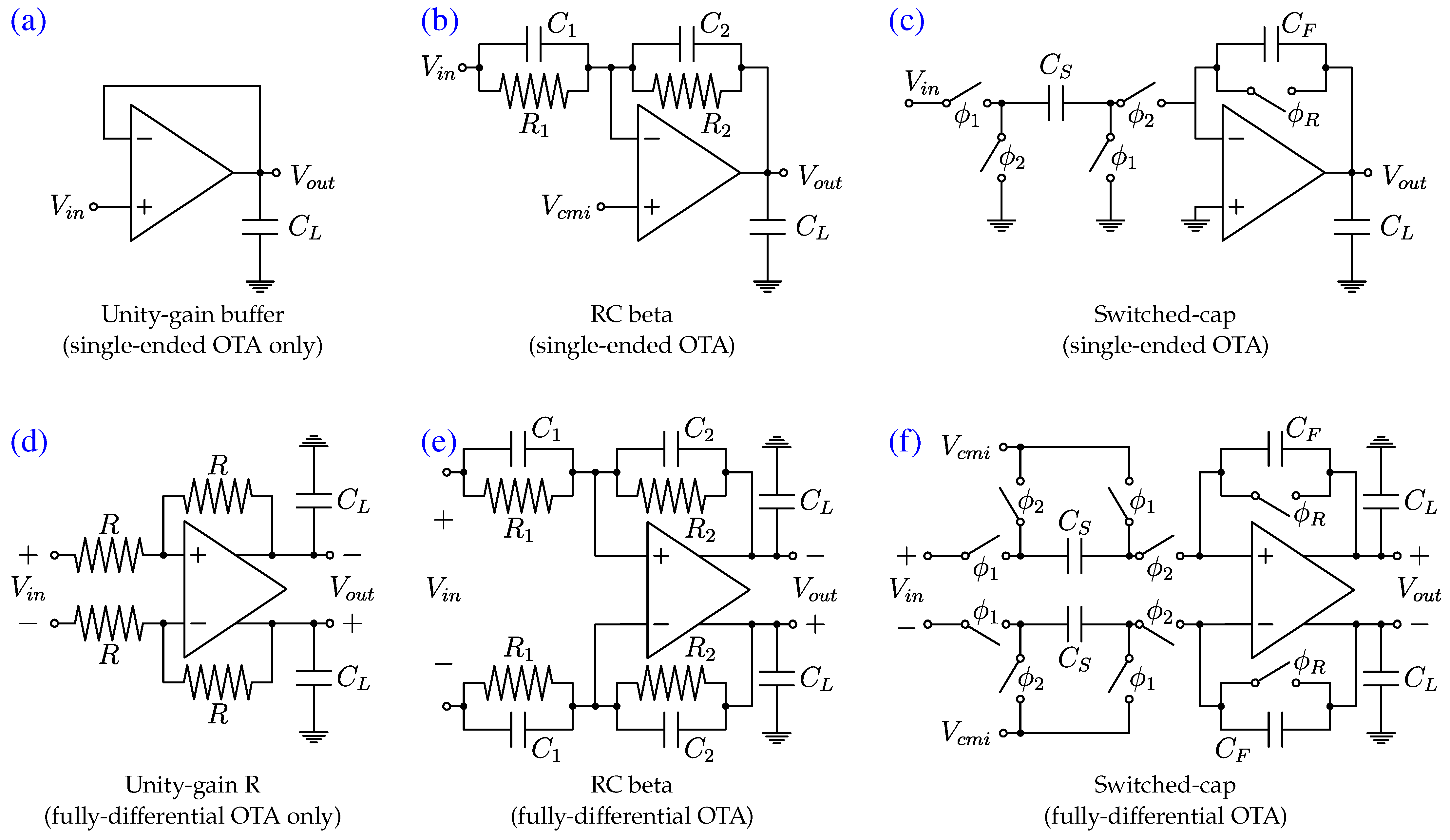
| Field | Variable | Units | Entry Type |
|---|---|---|---|
| Digital Object Identifier | DOI | Alphanumeric | |
| Title | TITL | Text | |
| First author | AU1 | Text | |
| Year | YEAR | Numeric (YYYY) | |
| CMOS technological node | CMOS | [nm] | Numeric |
| Number of gain stages | NS | Numeric | |
| Signal Configuration | SCFG | Either ‘Single-ended’ or ‘Fully-differential’ | |
| Test setup | TEST | Possible choices: ‘Not specified’, ‘RC-beta’, ‘Switched-cap configuration’, ‘Unity-gain buffer’, ‘Unity-gain R-beta’ | |
| Feedback factor () | BETA | Numeric | |
| Experimental method | EXPM | Either ‘Measured’ or ‘Simulated’ | |
| Effective capacitive load | CLE | [pF] | Numeric |
| Overall supply | SUP | [V] | Numeric |
| Input Voltage Step | DVS | [V] | Numeric |
| Positive Slew Rate | SRP | [V/µs] | Numeric |
| Negative Slew Rate | SRN | [V/µs] | Numeric |
| Unity-gain frequency | UGF | [MHz] | Numeric |
| Settling Time (positive step) | TSP | [ns] | Numeric |
| Settling Time (negative step) | TSN | [ns] | Numeric |
| Settling Error | SERR | [%] | Numeric |
| Power | PWR | [µW] | Numeric |
| Area | AREA | [mm2] | Numeric |
| Open-loop DC gain | A0 | [dB] | Numeric |
| Phase Margin | PM | [degree] | Numeric |
| Offset | OS | [mV] | Numeric |
| Spot Noise | SNOI | [nVrms/@kHz] | Numeric |
| Integrated Noise | INOI | [µVrms@kHz] | Numeric |
| (a) and (d) | (b) and (e) 1 | (c) and (f) | |
|---|---|---|---|
| BETA | 1 | ||
| CLE |
Disclaimer/Publisher’s Note: The statements, opinions and data contained in all publications are solely those of the individual author(s) and contributor(s) and not of MDPI and/or the editor(s). MDPI and/or the editor(s) disclaim responsibility for any injury to people or property resulting from any ideas, methods, instructions or products referred to in the content. |
© 2024 by the authors. Licensee MDPI, Basel, Switzerland. This article is an open access article distributed under the terms and conditions of the Creative Commons Attribution (CC BY) license (https://creativecommons.org/licenses/by/4.0/).
Share and Cite
Gagliardi, F.; Dei, M. Open and Collaborative Dataset for the Classification of Operational Transconductance Amplifiers for Switched-Capacitor Applications. Data 2024, 9, 114. https://doi.org/10.3390/data9100114
Gagliardi F, Dei M. Open and Collaborative Dataset for the Classification of Operational Transconductance Amplifiers for Switched-Capacitor Applications. Data. 2024; 9(10):114. https://doi.org/10.3390/data9100114
Chicago/Turabian StyleGagliardi, Francesco, and Michele Dei. 2024. "Open and Collaborative Dataset for the Classification of Operational Transconductance Amplifiers for Switched-Capacitor Applications" Data 9, no. 10: 114. https://doi.org/10.3390/data9100114
APA StyleGagliardi, F., & Dei, M. (2024). Open and Collaborative Dataset for the Classification of Operational Transconductance Amplifiers for Switched-Capacitor Applications. Data, 9(10), 114. https://doi.org/10.3390/data9100114