
In Silico Study of the Influence of Various Substrates on the Electronic Properties and Electrical Conductivity of Mono- and Bilayer Films of Armchair Single-Walled Carbon Nanotubes


Abstract
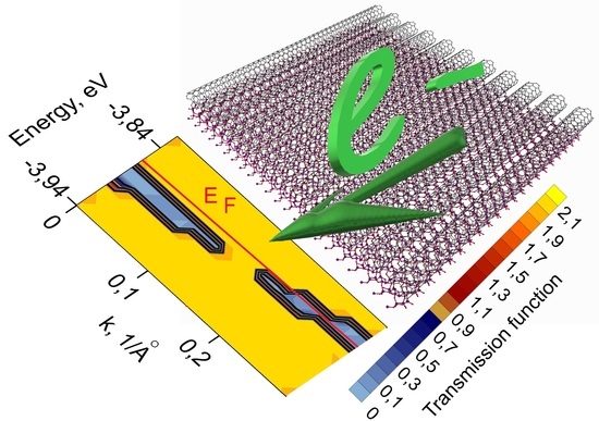
:
1. Introduction
2. Computational Details
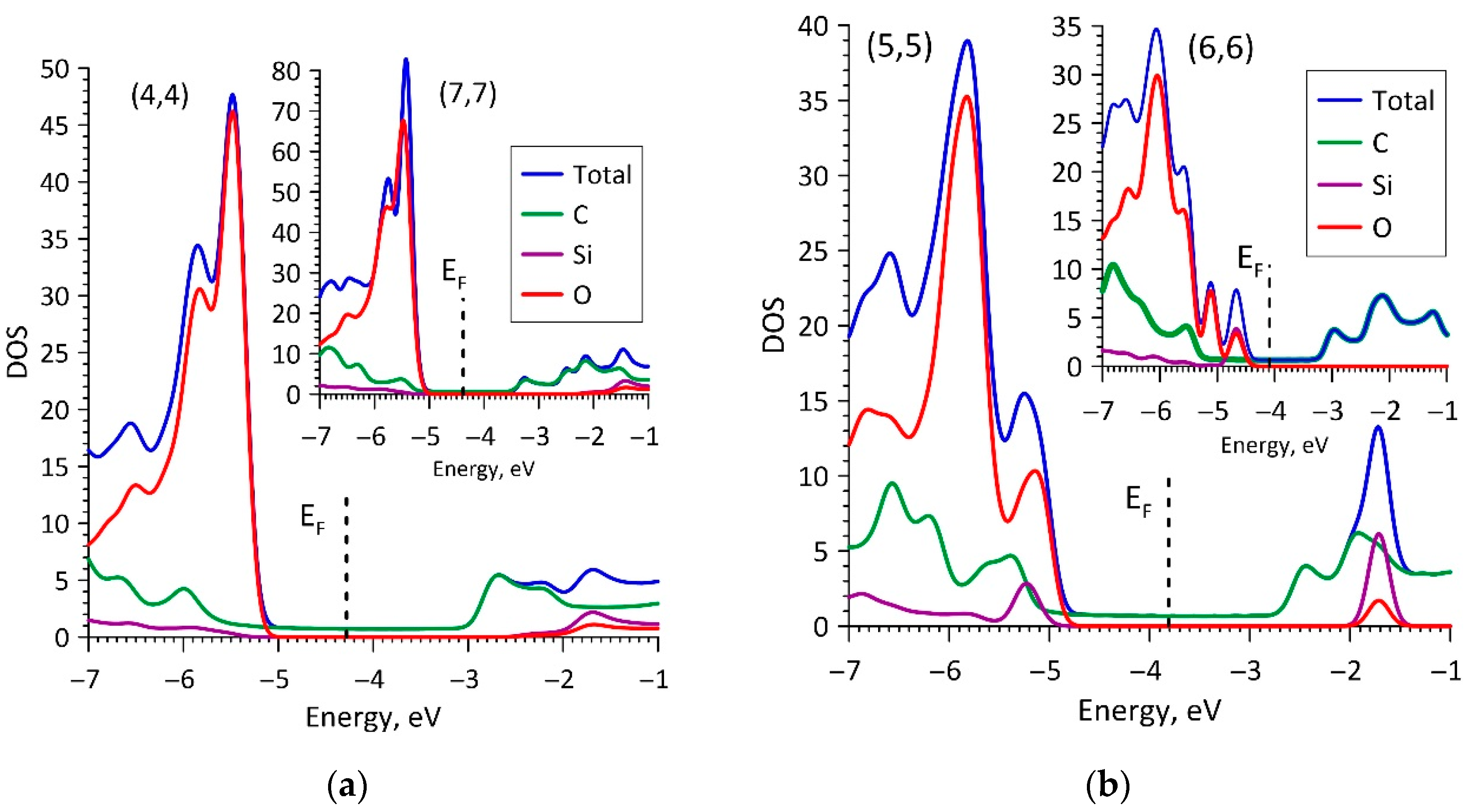
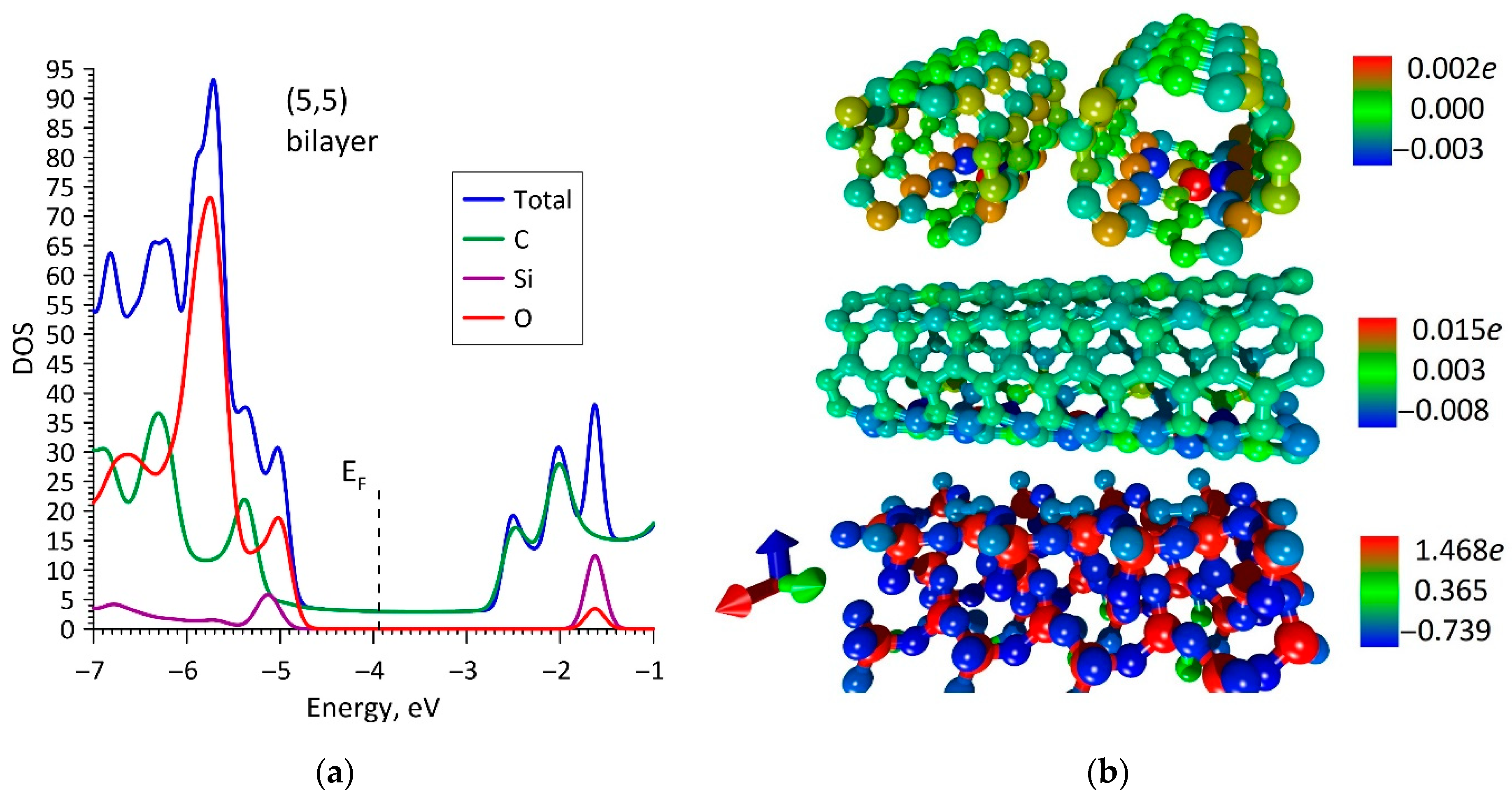
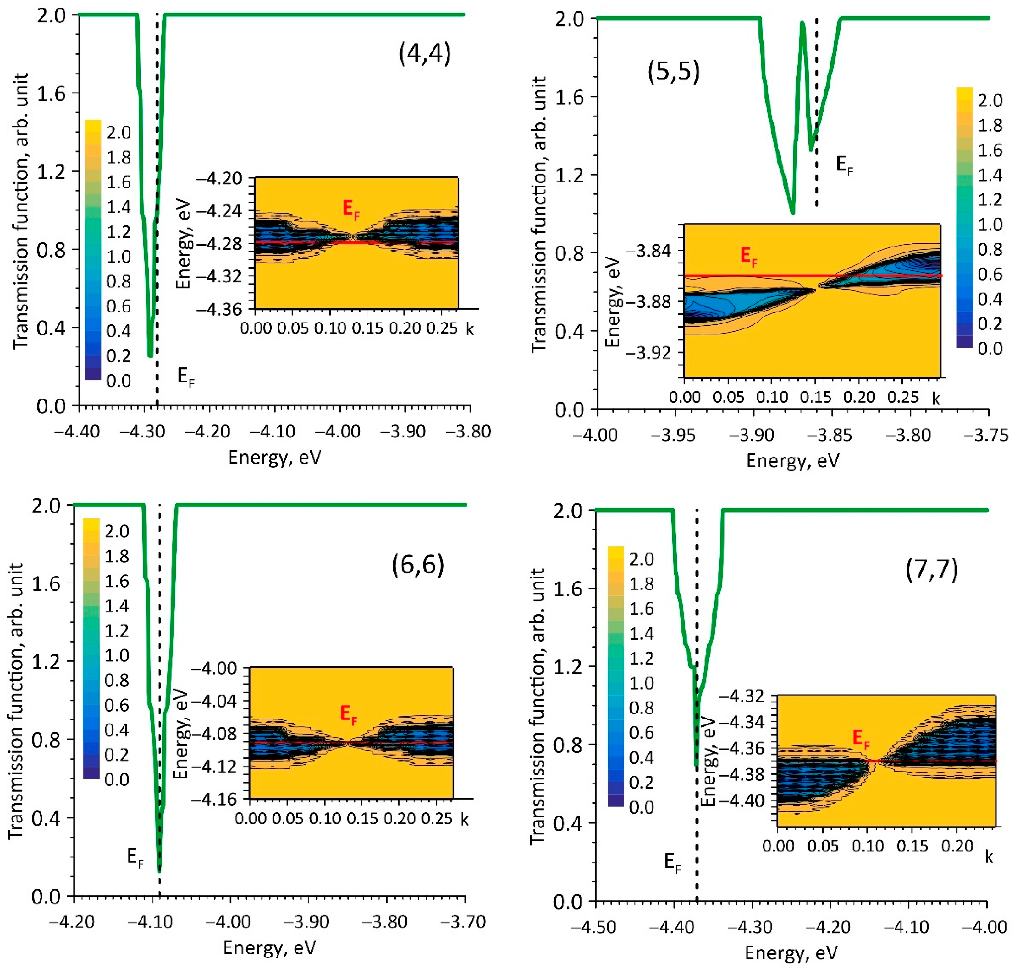
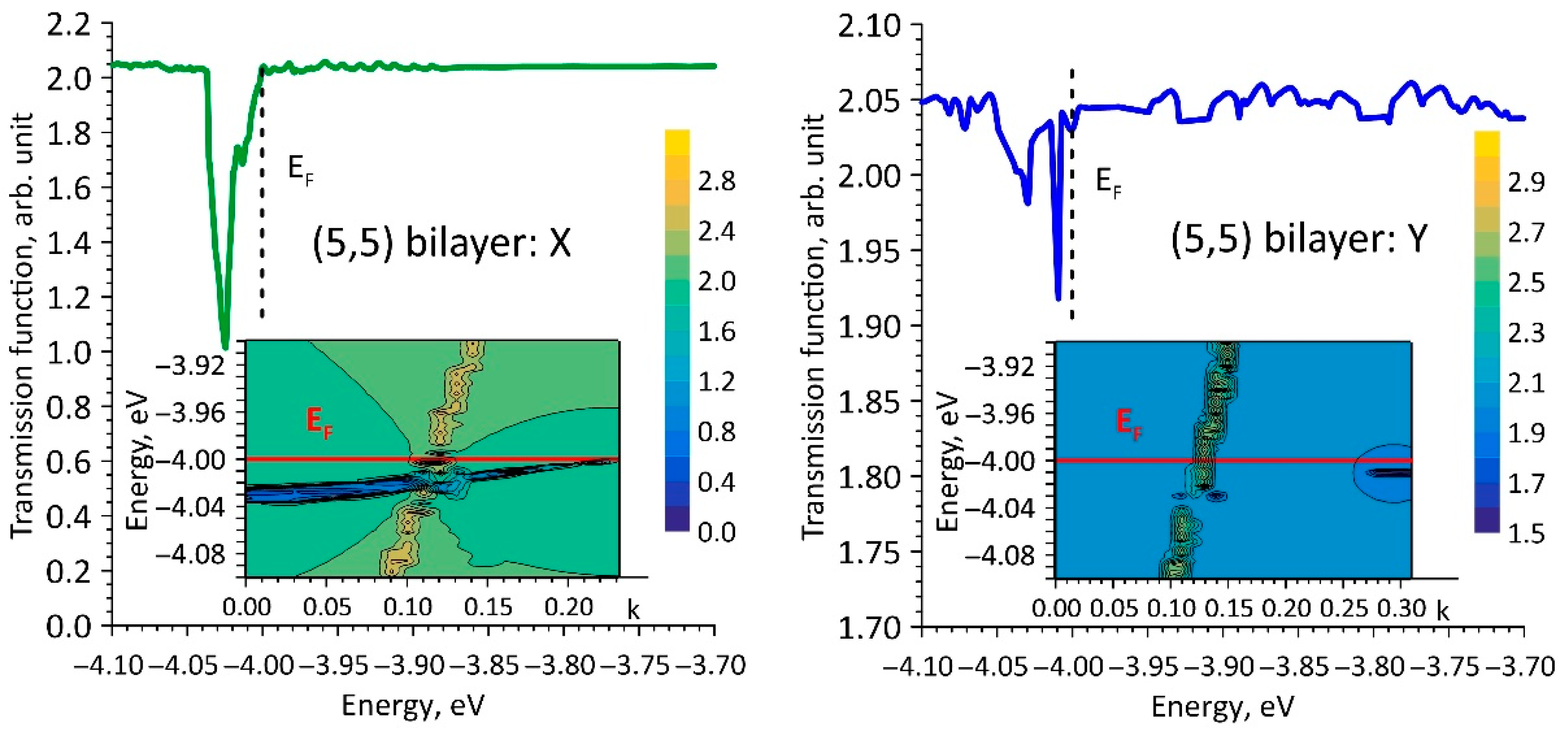
3. Results and Discussion
4. Conclusions
Author Contributions
Funding
Conflicts of Interest
References
- Jiang, S.; Hou, P.X.; Chen, M.L.; Wang, B.W.; Sun, D.M.; Tang, D.M.; Jin, Q.; Guo, Q.X.; Zhang, D.D.; Du, J.H.; et al. Ultrahigh-performance transparent conductive films of carbon-welded isolated single-wall carbon nanotubes. Sci. Adv. 2018, 4, eaap9264. [Google Scholar] [CrossRef] [PubMed] [Green Version]
- Devaraju, S.; Lee, T.; Mohanty, A.K.; Hong, Y.K.; Yoon, K.H.; Lee, Y.S.; Han, J.H.; Paik, H.J. Fabrication of durable and flexible single-walled carbon nanotube transparent conductive films. RSC Adv. 2017, 7, 19267–19272. [Google Scholar] [CrossRef] [Green Version]
- Siwal, S.S.; Saini, A.K.; Rarotra, S.; Zhang, Q.; Thakur, V. Recent advancements in transparent carbon nanotube films: Chemistry and imminent challenges. J. Nanostruct. Chem. 2021, 11, 93–130. [Google Scholar] [CrossRef]
- Qu, S.; Dai, Y.; Zhang, D.; Li, Q.; Chou, T.; Weibang, L. Carbon nanotube film based multifunctional composite materials: An overview. Funct. Compos. Struct. 2020, 2, 022002. [Google Scholar] [CrossRef]
- Zhang, Q.; Zhou, W.; Xia, X.; Li, K.; Zhang, N.; Wang, Y.; Xiao, Z.; Fan, Q.; Kauppinen, E.; Xie, S. Transparent and Freestanding Single-Walled Carbon Nanotube Films Synthesized Directly and Continuously via a Blown Aerosol Technique. Adv. Mater. 2020, 32, 2004277. [Google Scholar] [CrossRef] [PubMed]
- Mirri, F.; Ma, A.W.; Hsu, T.T.; Behabtu, N.; Eichmann, S.L.; Young, C.C.; Tsentalovich, D.E.; Pasquali, M. High-Performance Carbon Nanotube Transparent Conductive Films by Scalable Dip Coating. ACS Nano 2012, 6, 9737–9744. [Google Scholar] [CrossRef]
- Shimoni, A.; Azoubel, S.; Magdassi, S. Inkjet printing of flexible high-performance carbon nanotube transparent conductive films by “coffee ring effect”. Nanoscale 2014, 6, 11084–11089. [Google Scholar] [CrossRef] [PubMed]
- Yu, W.; Zhou, H.; Li, B.Q.; Ding, S. 3D Printing of Carbon Nanotubes-Based Microsupercapacitors. ACS Appl. Mater. Interfaces 2017, 9, 4597–4604. [Google Scholar] [CrossRef]
- Sweeney, C.B.; Lackey, B.A.; Pospisil, M.J.; Achee, T.C.; Hicks, V.K.; Moran, A.G.; Teipel, B.R.; Saed, M.A.; Green, M.J. Welding of 3D-printed carbon nanotube–polymer composites by locally induced microwave heating. Sci. Adv. 2017, 3, e1700262. [Google Scholar] [CrossRef] [PubMed] [Green Version]
- Mustonen, K.; Nasibulin, A.G.; Pudas, M.; Kauppinen, M.; Jiang, H.; Grigoras, K.; Raula, J.; Kauppinen, E.I. Reinforcing randomly oriented transparent freestanding single-walled carbon nanotube films. Carbon 2013, 62, 513–516. [Google Scholar] [CrossRef]
- Bu, Q.; Zhan, Y.; He, F.; Lavorgna, M.; Xia, H. Stretchable conductive films based on carbon nanomaterials prepared by spray coating. J. Appl. Polym. Sci. 2016, 133, 43243. [Google Scholar] [CrossRef]
- De Volder, M.F.; Tawfick, S.H.; Baughman, R.H.; Hart, A.J. Carbon nanotubes: Present and future commercial applications. Science 2013, 339, 535–539. [Google Scholar] [CrossRef] [Green Version]
- Zhou, Y.; Azumi, R. Carbon nanotube based transparent conductive films: Progress, challenges, and perspectives. Sci. Technol. Adv. Mater. 2016, 17, 493–516. [Google Scholar] [CrossRef] [Green Version]
- Huang, J.; Zhu, Y.; Jiang, W.; Yin, J.; Tang, Q.; Yang, X. Parallel carbon nanotube stripes in polymer thin film with remarkable conductive anisotropy. ACS Appl. Mater. Interfaces 2014, 6, 1754–1758. [Google Scholar] [CrossRef]
- Dong, C.; Hao, J. Ordered porous films of single-walled carbon nanotubes using an ionic exchange reaction. Colloids Surf. A Physicochem. Eng. Asp. 2019, 566, 207–217. [Google Scholar] [CrossRef]
- Sajed, F.; Rutherglen, C. All-printed and transparent single walled carbon nanotube thin film transistor devices. Appl. Phys. Lett. 2013, 103, 143303. [Google Scholar] [CrossRef]
- Bandodkar, A.J.; Jeerapan, I.; You, J.M.; Nuñez-Flores, R.; Wang, J. Highly Stretchable Fully-Printed CNT-Based Electrochemical Sensors and Biofuel Cells: Combining Intrinsic and Design-Induced Stretchability. Nano Lett. 2016, 16, 721–727. [Google Scholar] [CrossRef] [PubMed] [Green Version]
- Wang, C.; Takei, K.; Takahashi, T.; Javey, A. Carbon nanotube electronics—Moving forward. Chem. Soc. Rev. 2013, 42, 2592–2609. [Google Scholar] [CrossRef]
- Cai, L.; Wang, C. Carbon Nanotube Flexible and Stretchable Electronics. Nanoscale Res. Lett. 2015, 10, 320. [Google Scholar] [CrossRef] [PubMed] [Green Version]
- Cai, L.; Song, L.; Luan, P.; Zhang, Q.; Zhang, N.; Gao, Q.; Zhao, D.; Zhang, X.; Tu, M.; Yang, F.; et al. Super-stretchable, transparent carbon nanotube-based capacitive strain sensors for human motion detection. Sci. Rep. 2013, 3, 3048. [Google Scholar] [CrossRef] [Green Version]
- Dinh, T.; Phan, H.P.; Nguyen Tuan, K.; Qamar, A.; Md Foisal, A.; Viet, T.N.; Tran, C.D.; Zhu, Y.; Nguyen, N.T.; Dao, D. Environment-friendly carbon nanotube based flexible electronics for noninvasive and wearable healthcare. J. Mater. Chem. C 2016, 4, 10061–10068. [Google Scholar] [CrossRef]
- Lv, X.; Deng, J.; Wang, B.; Zhong, J.; Sham, T.K.; Sun, X.; Sun, X. γ-Fe2O3@CNTs Anode Materials for Lithium Ion Batteries Investigated by Electron Energy Loss Spectroscopy. Chem. Mater. 2017, 29, 3499–3506. [Google Scholar] [CrossRef]
- Franklin, A.D.; Chen, Z.H. Length scaling of carbon nanotube transistors. Nat. Nanotech. 2010, 5, 858–862. [Google Scholar] [CrossRef]
- Franklin, A.D.; Luisier, M.; Han, S.J.; Tulevski, G.; Breslin, C.M.; Gignac, L.; Lundstrom, M.S.; Haensch, W. Sub-10 nm carbon nanotube transistor. Nano. Lett. 2012, 12, 758–762. [Google Scholar] [CrossRef] [PubMed]
- Qiu, C.; Zhang, Z.; Xiao, M.; Yang, Y.; Zhong, D.; Peng, L. Scaling carbon nanotube complementary transistors to 5-nm gate lengths. Science 2017, 355, 271–276. [Google Scholar] [CrossRef]
- Xu, L.; Qiu, C.; Peng, L.-M.; Zhang, Z. Suppression of leakage current in carbon nanotube field-effect transistors. Nano Res. 2021, 14, 976–981. [Google Scholar] [CrossRef]
- Franklin, A.D. Te road to carbon nanotube transistors. Nature 2013, 498, 443–444. [Google Scholar] [CrossRef] [PubMed]
- Zhong, D.; Zhang, Z.; Ding, L.; Han, J.; Xiao, M.; Si, J.; Xu, L.; Qiu, C.; Peng, L. Gigahertz integrated circuits based on carbon nanotube films. Nat. Electron. 2018, 1, 40–45. [Google Scholar] [CrossRef]
- Xie, Y.; Zhang, Z.; Zhong, D.; Peng, L. Speeding up carbon nanotube integrated circuits through three-dimensional architecture. Nano Res. 2019, 12, 1810–1816. [Google Scholar] [CrossRef]
- Liu, L.; Ding, L.; Zhong, D.; Han, J.; Wang, S.; Meng, Q.; Qiu, C.; Zhang, X.; Peng, L.M.; Zhang, Z. Carbon Nanotube Complementary Gigahertz Integrated Circuits and Their Applications on Wireless Sensor Interface Systems. ACS Nano 2019, 13, 2526–2535. [Google Scholar] [CrossRef]
- Liu, Z.; Zhao, J.; Xu, W.; Qian, L.; Nie, S.; Cui, Z. Effect of surface wettability properties on the electrical properties of printed carbon nanotube thin-film transistors on SiO2/Si substrates. ACS Appl. Mater. Interfaces 2014, 6, 9997–10004. [Google Scholar] [CrossRef]
- Xiang, L.; Zhang, H.; Dong, G.; Zhong, D.; Han, J.; Liang, X.; Zhang, Z.; Peng, L.-M.; Hu, Y. Low-Power Carbon Nanotube-Based Integrated Circuits that Can be Transferred to Biological Surface. Nat. Electron. 2018, 1, 237–245. [Google Scholar] [CrossRef]
- Li, X.; Zhu, Y.; Cai, W.; Borysiak, M.; Han, B.; Chen, D.; Piner, R.D.; Colombo, L.; Ruoff, R.S. Transfer of Large-Area Graphene Films for High-Performance Transparent Conductive Electrodes. Nano Lett. 2009, 9, 4359–4363. [Google Scholar] [CrossRef] [PubMed]
- Liu, S.; Guo, X. Carbon nanomaterials field-effect-transistor-based biosensors. NPG Asia Mater. 2012, 4, e23. [Google Scholar] [CrossRef] [Green Version]
- Elstner, M.; Porezag, D.; Jungnickel, G.; Elsner, J.; Haugk, M.; Frauenheim, T.; Suhai, S.; Seifert, G. Self-consistent-charge density-functional tight-binding method for simulations of complex materials properties. Phys. Rev. B 1998, 58, 7260–7268. [Google Scholar] [CrossRef]
- Elstner, M.; Seifert, G. Density functional tight binding. Phil. Trans. R. Soc. A 2014, 372, 20120483. [Google Scholar] [CrossRef] [Green Version]
- Ghorbani-Asl, M.; Bristowe, P.D.; Koziol, K. A computational study of the quantum transport properties of a Cu-CNT composite. Phys. Chem. Chem. Phys. 2015, 17, 18273–18277. [Google Scholar] [CrossRef] [Green Version]
- Naumov, V.S.; Loginova, A.S.; Avdoshin, A.A.; Ignatov, S.; Mayorov, A.V.; Aradi, B.; Frauenheim, T. Structural, electronic, and thermodynamic properties of TiO2/organic clusters: Performance of DFTB method with different parameter sets. Int. J. Quantum Chem. 2021, 121, e26427. [Google Scholar] [CrossRef]
- Slepchenkov, M.M.; Shmygin, D.S.; Zhang, G.; Glukhova, O.E. Controlling anisotropic electrical conductivity in porous graphene-nanotube thin films. Carbon 2020, 165, 139–149. [Google Scholar] [CrossRef]
- Rappe, A.K.; Casewit, C.J.; Colwell, K.S.; Goddard III, W.A.; Skiff, W.M. UFF, a full periodic table force field for molecular mechanics and molecular dynamics simulations. J. Am. Chem. Soc. 1992, 114, 10024–10035. [Google Scholar] [CrossRef]
- DFTB+ Density Functional Based Tight Binding (and More). Available online: https://dftbplus.org/ (accessed on 10 October 2020).
- Hourahine, B.; Aradi, B.; Blum, V.; Bonafé, F.; Buccheri, A.; Camacho, C.; Cevallos, C.; Deshaye, M.Y.; Dumitrică, T.; Dominguez, A.; et al. DFTB+, a software package for efficient approximate density functional theory based atomistic simulations. J. Chem. Phys. 2020, 152, 124101. [Google Scholar] [CrossRef]
- Datta, S. Quantum Transport.: Atom. to Transistor, 2nd ed.; Cambridge University Press: New York, NY, USA, 2005; pp. 217–251. [Google Scholar]
- Glukhova, O.E.; Shmygin, D.S. The electrical conductivity of CNT/graphene composites: A new method for accelerating transmission function calculations. Beilstein. J. Nanotechnol. 2018, 9, 1254–1262. [Google Scholar] [CrossRef]
- Software Package Mizar. Available online: Nanokvazar.ru/ (accessed on 8 November 2020).

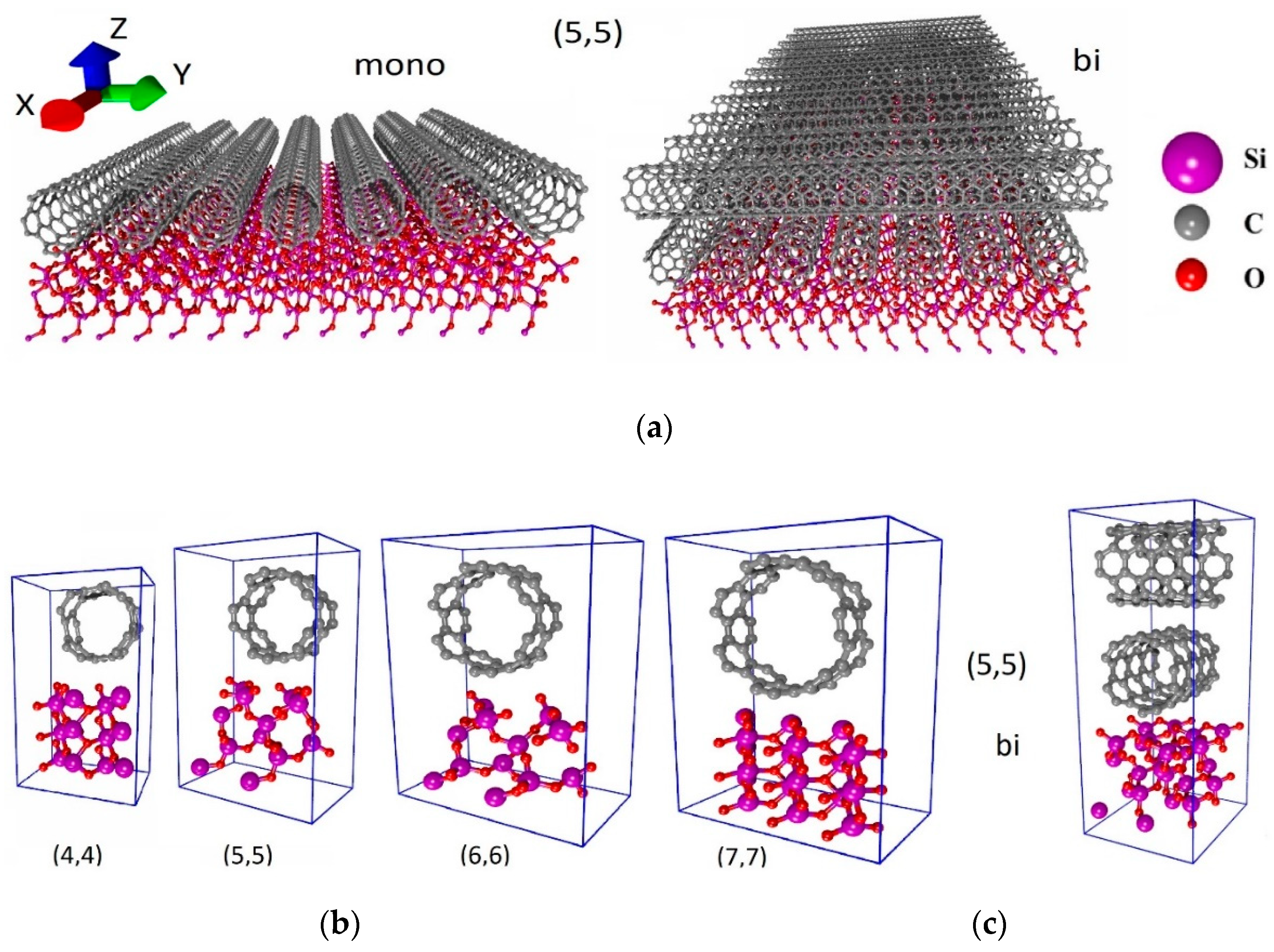
| Parameters | Qtube, |e| | Nat | Nat(SiO2) | |||
|---|---|---|---|---|---|---|
| Monolayer Film | ||||||
| (4,4) | 8.82 | 4.92 | −0.0021 | −4.28 | 68 | 36 |
| (5,5) | 10.18 | 4.92 | −0.0034 | −3.86 | 76 | 36 |
| (6,6) | 11.54 | 4.92 | −0.0023 | −4.09 | 84 | 36 |
| (7,7) | 12.9 | 4.92 | −0.0079 | −4.37 | 110 | 54 |
| Bilayer Film | ||||||
| (5,5) | 10.18 | 10.18 | −0.0229 | −3.98 | 232 | 72 |
| Parameters | (4,4) | (5,5) | (6,6) | (7,7) | (5,5)-X Bilayer | (5,5)-Y Bilayer |
|---|---|---|---|---|---|---|
| Films on a Substrate | ||||||
| G, μS | 123.824 | 132.686 | 144.638 | 123.528 | 148.005 | 155.312 |
| R, kOhm | 8.076 | 7.537 | 6.913 | 8.095 | 6.800 | 6.438 |
| Films without Backing | ||||||
| G, μS | 121.045 | 145.619 | 134.027 | 144.914 | 155.312 | 155.312 |
| R, kOhm | 8.261 | 6.867 | 7.461 | 6.900 | 6.438 | 6.431 |
Publisher’s Note: MDPI stays neutral with regard to jurisdictional claims in published maps and institutional affiliations. |
© 2021 by the authors. Licensee MDPI, Basel, Switzerland. This article is an open access article distributed under the terms and conditions of the Creative Commons Attribution (CC BY) license (https://creativecommons.org/licenses/by/4.0/).
Share and Cite
Slepchenkov, M.M.; Petrunin, A.A.; Glukhova, O.E. In Silico Study of the Influence of Various Substrates on the Electronic Properties and Electrical Conductivity of Mono- and Bilayer Films of Armchair Single-Walled Carbon Nanotubes. ChemEngineering 2021, 5, 48. https://doi.org/10.3390/chemengineering5030048
Slepchenkov MM, Petrunin AA, Glukhova OE. In Silico Study of the Influence of Various Substrates on the Electronic Properties and Electrical Conductivity of Mono- and Bilayer Films of Armchair Single-Walled Carbon Nanotubes. ChemEngineering. 2021; 5(3):48. https://doi.org/10.3390/chemengineering5030048
Chicago/Turabian StyleSlepchenkov, Michael M., Alexander A. Petrunin, and Olga E. Glukhova. 2021. "In Silico Study of the Influence of Various Substrates on the Electronic Properties and Electrical Conductivity of Mono- and Bilayer Films of Armchair Single-Walled Carbon Nanotubes" ChemEngineering 5, no. 3: 48. https://doi.org/10.3390/chemengineering5030048
APA StyleSlepchenkov, M. M., Petrunin, A. A., & Glukhova, O. E. (2021). In Silico Study of the Influence of Various Substrates on the Electronic Properties and Electrical Conductivity of Mono- and Bilayer Films of Armchair Single-Walled Carbon Nanotubes. ChemEngineering, 5(3), 48. https://doi.org/10.3390/chemengineering5030048