
Article

Balancing Conductive Network Continuity and Out-of-Plane Transport Barrier in PEDOT:PSS/Ga2O3 Self-Powered Solar-Blind Photoelectrochemical Photodetectors


1
State Key Laboratory of Luminescent Materials and Devices, Guangdong Basic Research Center of Excellence for Energy & Information Polymer Materials, School of Materials Sciences and Engineering, South China University of Technology, Guangzhou 510640, China
2
Huangpu Hydrogen Innovation Center, School of Chemistry and Chemical Engineering, Guangzhou University, Guangzhou 510006, China
3
Science and Technology on Reliability Physics and Application Technology of Electronic Component Laboratory, Guangzhou 511370, China
4
ShenZhen Yaham Optoelectronics, Co., Ltd., Shenzhen 518103, China
5
Department of Engineering, University of Cambridge, Cambridge CB3 OFA, UK
*
Authors to whom correspondence should be addressed.
Inorganics 2026, 14(8), 209; https://doi.org/10.3390/inorganics14080209
Submission received: 24 June 2026 / Revised: 28 July 2026 / Accepted: 3 August 2026 / Published: 6 August 2026
(This article belongs to the Special Issue Advanced Inorganic Semiconductor Materials, 4th Edition)

Abstract

To realize self-powered solar-blind ultraviolet (UV) photodetectors with high stability, high efficiency, and low cost, a self-powered photoelectrochemical (PEC)-type hybrid UV photodetector was constructed based on a poly(3,4-ethylenedioxythiophene):polystyrene sulfonate (PEDOT:PSS)/Ga2O3 organic–inorganic heterojunction. The PEDOT:PSS layer serves not only as a p-type hole transport layer but also as an interface modification layer to modulate charge separation and surface recombination in Ga2O3. As the spin-coating speed decreases, the PEDOT:PSS film thickness increases monotonically from 33.27 to 44.18 nm. Thicker films develop a more continuous conductive network, which favors hole transport. However, additional insulating PSS lamellae also accumulate in the vertical direction, creating a higher out-of-plane transport barrier that counteracts this improvement. The device with an intermediate film thickness of 36.50 nm achieves the optimal balance between these two competing factors, delivering a responsivity of 20.6 mA/W and a specific detectivity of 1.36 × 10¹⁰ Jones under 267 nm illumination at zero bias, along with a high UV/visible rejection ratio of 3.18 × 10⁵ and fast rise/decay times of 26/10 ms. This work provides a facile interface engineering strategy for low-cost, high-performance self-powered solar-blind UV photodetectors.

1. Introduction

The solar-blind ultraviolet (UV) band (200–280 nm) is strongly absorbed by atmospheric ozone and water vapor, resulting in negligible background light interference at the Earth’s surface. This unique property endows solar-blind UV photodetectors with ultrahigh sensitivity and strong anti-interference capability, making them highly valuable in civil, military, and scientific research fields [1,2,3,4]. Conventional UV detectors rely on external bias voltages to separate photogenerated carriers, which leads to high power consumption, large dark current, and complex circuitry, limiting their applications in remote areas and portable devices [5]. In contrast, self-powered detectors based on the built-in electric field of heterojunctions require no external power supply, aligning perfectly with the development trend of low power consumption and portability, and have thus become a current research hotspot [6,7,8,9].
Gallium oxide (Ga2O3), as an ultra-wide bandgap semiconductor with a bandgap of 4.5–5.3 eV, intrinsically covers the solar-blind UV band. It also possesses excellent chemical and thermal stability and can be fabricated via low-cost processes such as the hydrothermal method [10,11,12]. However, solution-processed Ga2O3 generally suffers from abundant surface defects and low carrier separation efficiency, which severely restrict its detection performance [13,14]. Most existing self-powered detectors based on inorganic heterojunctions are fabricated by high-vacuum and high-temperature techniques. These techniques require expensive equipment and are difficult to scale up for mass production. For example, Fang et al. prepared ZnO/Ga2O3 core–shell nanowire heterojunctions via a two-step chemical vapor deposition (CVD) method [15]; An et al. synthesized p-Si/n-Ga2O3 and p-Si/i-SiC/n-Ga2O3 heterojunctions using laser molecular beam epitaxy technology [16]. In comparison, organic–inorganic heterojunctions combine the low-cost advantage of solution processing with the excellent optoelectronic properties of inorganic materials, making them a highly promising development direction. For instance, Sun et al. reported a self-powered solar-blind photodetector based on a polyaniline/a-Ga2O3 hybrid heterojunction [17]; Wang et al. reported a multifunctional solar-blind photodetector based on p-type poly[N-90-heptadecanyl-2,7-carbazole-alt-5,5-(40,70-di-2-thienyl-20,10,30-benzothiadiazole)] (PCDTBT)/n-type a-Ga2O3 [18]. Although these solution-processed organic–inorganic heterojunctions have demonstrated the feasibility of low-cost self-powered detection, the organic layer thickness has typically been chosen empirically. The nanoscale quality of the organic–inorganic interface is a recognized determinant of charge transport and device performance in various optoelectronic and energy systems [19,20,21,22]. However, it has not been explicitly examined in Ga2O3-based photodetectors.
Among numerous organic functional materials, poly(3,4-ethylenedioxythiophene):polystyrene sulfonate (PEDOT:PSS) stands out due to its well-balanced comprehensive performance and is one of the most widely used conductive polymers today. It exhibits water solubility, high optical transparency, and tunable work function, making it an ideal hole transport material for constructing high-performance photodetectors [23,24]. When forming a heterojunction with n-type Ga2O3, PEDOT:PSS can simultaneously act as a hole transport layer and an interface modification layer, promoting charge separation and passivating surface defects. However, an excessively thick PEDOT:PSS film will increase the out-of-plane transport barrier, which rises monotonically with increasing film thickness; conversely, an overly thin film cannot form a continuous conductive network, leading to a decline in hole transport capability [25,26]. Therefore, we hypothesize that maximizing device performance requires a delicate balance between these two thickness-governed transport properties: the continuity of the conductive network and the out-of-plane transport barrier.
To test the hypothesis, we fabricated PEDOT:PSS/Ga2O3 organic–inorganic heterojunction photodetectors with systematically varied PEDOT:PSS thicknesses via controlled spin-coating. Our results confirm that the device performance exhibits a non-monotonic dependence on film thickness. The optimal device, fabricated at 4000 rpm with a thickness of 36.50 nm, achieves a responsivity of 20.6 mA/W and a specific detectivity of 1.36 × 10¹⁰ Jones under 267 nm illumination at zero bias, along with an excellent UV/visible rejection ratio R267/R405 of 3.18 × 10⁵, fast response speed of 26/10 ms, and good environmental stability.

2. Experimental

2.1. Preparation of PEDOT:PSS Thin Films

To characterize the intrinsic morphology, optical and structural properties of PEDOT:PSS films, pristine PEDOT:PSS single-layer films were first fabricated on bare indium tin oxide (ITO)/quartz substrates as reference samples. The PEDOT:PSS solution (Clevios P VP AI 4083, Heraeus, Hanau, Germany) was first ultrasonically dispersed in an ice-water bath for 10 min, and then filtered through a 0.45 μm aqueous syringe filter to remove insoluble impurities. The ITO or quartz substrate was treated with plasma for 15 min to introduce hydroxyl groups and improve the wettability of the substrate for PEDOT:PSS. Subsequently, 35 μL of the filtered solution was pipetted onto the substrate. Spin-coating was then performed at a low speed of 500 rpm for 6 s, followed by a high-speed step at 2000, 3000, 4000, or 5000 rpm for 40 s. Finally, the sample was annealed at 150 °C for 15 min to obtain the PEDOT:PSS thin film.

2.2. Preparation of the Ultraviolet Photodetector

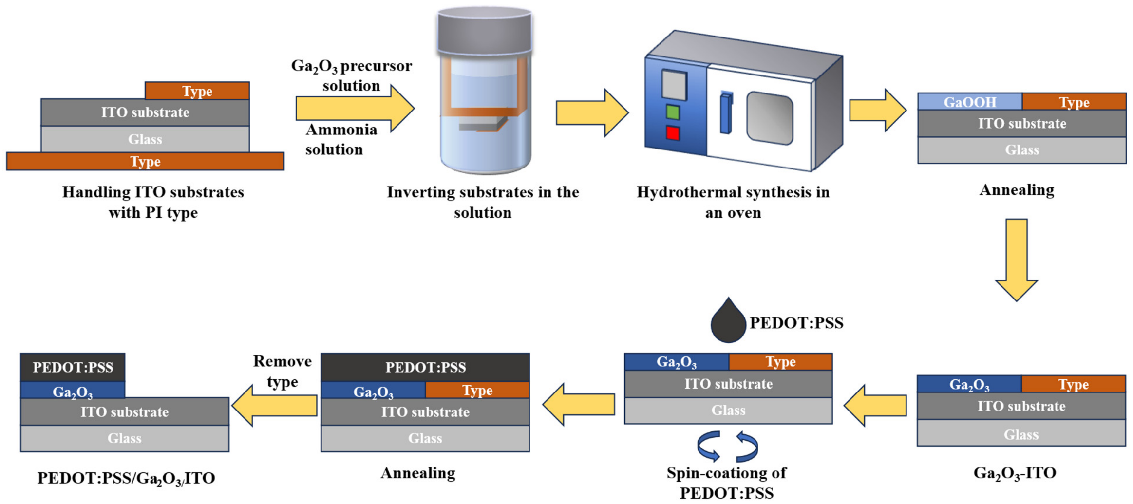
Ga2O3 thin films prepared from a 0.06 M precursor solution via 24 h hydrothermal treatment exhibit excellent photoelectric properties [27]. A schematic diagram of the complete fabrication process is given in Figure 1. 0.2302 g of gallium nitrate hydrate (Ga(NO3)3, Shanghai Macklin Biochemical Co., Ltd., Shanghai, China, 99.99% metals basis) was dissolved in 15 mL of deionized water. The pH of the solution was adjusted to 5 with ammonia solution, and the mixture was stirred for 1 h to obtain the precursor solution. The substrate was first subjected to plasma treatment for 10 min to promote the nucleation and growth of Ga2O3 on the ITO glass substrate (10 mm × 10 mm). The treated substrate was then placed face-down in a glass vial; half of its front surface was covered with polyimide (PI) tape to keep a portion of the ITO exposed as the electrode. The vial was transferred to a drying oven (DGG 9030A, Shanghai Pain Laboratory Instrument Co., Ltd., Shanghai, China) and kept at 90 °C for 24 h. After the hydrothermal reaction, the substrate was removed, rinsed with deionized water, and blown dry with nitrogen. The resulting film was dried at 150 °C for 10 min and subsequently annealed at 500 °C for 2 h to obtain the Ga2O3 thin film. Finally, the Ga2O3-coated substrate was subjected to a brief plasma treatment for 10 min to improve the wettability of the oxide surface. A PEDOT:PSS layer was then deposited onto the treated Ga2O3 film by spin-coating, using the same coating parameters as those described in Section 2.1, forming the PEDOT:PSS/Ga2O3 heterojunction device.

2.3. Characterization of Thin Films

The surface morphology of the PEDOT:PSS thin films was observed by atomic force microscopy (AFM, CSPM 5500, Benyuan Nano-Instruments, Ltd., Guangzhou, China) and confocal laser scanning microscopy (LCSM, LEXT OLS 5000, Olympus Corporation, Tokyo, Japan). The absorbance of the PEDOT:PSS thin films was measured by an ultraviolet-visible spectrophotometer (Shimadzu UV2860, Shimadzu Corporation, Kyoto, Japan). The Fourier-transform infrared spectroscopy (FTIR) of the PEDOT:PSS thin films were recorded on a SHIMADZU IR Prestige21 in transmission mode using quartz substrates. The crystallinity of the PEDOT:PSS thin films and Ga2O3 films was characterized by X-ray diffraction (XRD, Empyrean DY1577, PANalytical B.V., Almelo, Netherlands) with Cu Kα radiation (0.1542 nm). Scanning electron microscopy (SEM) and energy-dispersive X-ray spectroscopy (EDS) were performed using a Thermo Scientific Helios 5 DualBeam system (Thermo Fisher Scientific, Hillsboro, OR, USA). X-ray photoelectron spectroscopy (XPS) measurements were performed on a Thermo Scientific Nexsa spectrometer (Thermo Fisher Scientific, Waltham, MA, USA) using monochromatic Al Kα radiation (1486.6 eV).

2.4. Photoelectrochemical (PEC) Measurements of PEDOT:PSS/Ga2O3 Heterojunction Devices

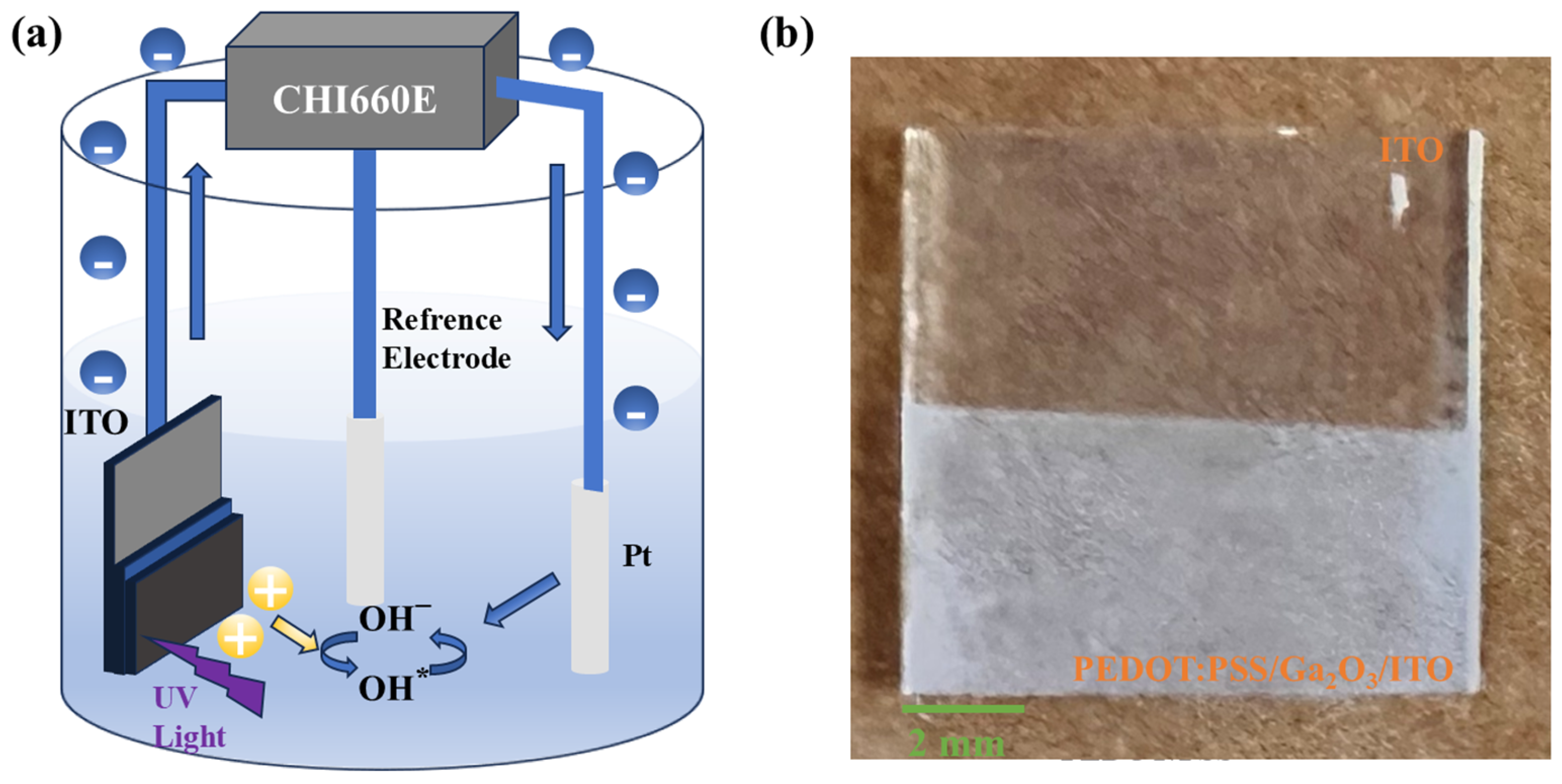
As shown in Figure 2a, an electrochemical setup was constructed to test the photoelectric performance of the prepared device. In this setup, the ITO glass substrate coated with the PEDOT:PSS/Ga2O3 heterojunction served as the photoanode, and a platinum (Pt) wire served as the counter electrode. A silver/silver chloride (Ag/AgCl) electrode was used as the reference, and a 0.1 M Na2SO4 solution was chosen as the electrolyte to ensure the stability of the electrochemical test system and the reliability of the test results. The electrical properties of the PEDOT:PSS/Ga2O3 heterojunction devices (Figure 2b) were investigated using an electrochemical workstation (CHI660E, Shanghai Chenhua Instrument Co., Ltd., Shanghai, China). The 267 nm light source used in the test was divided into four intensity levels (I, II, III, IV), corresponding to optical irradiances of 0.866, 1.847, 3.310, and 4.350 mW/cm2, respectively; in the spectral selectivity test, the light intensities of the 267, 365, 385, and 405 nm LED light sources were set to 4, 108, 46, and 680 mW/cm2, respectively. All photoelectrochemical measurements were performed under zero external bias (0 V vs. Ag/AgCl), with the device operating in the self-powered mode. The device-level performance metrics reported in the text (responsivity, detectivity) were based on three repeated measurements on the same representative device for each fabrication condition.

3. Results and Discussion

3.1. Phase and Morphology of α-Ga2O3 and PEDOT:PSS/α-Ga2O3 Heterostructures

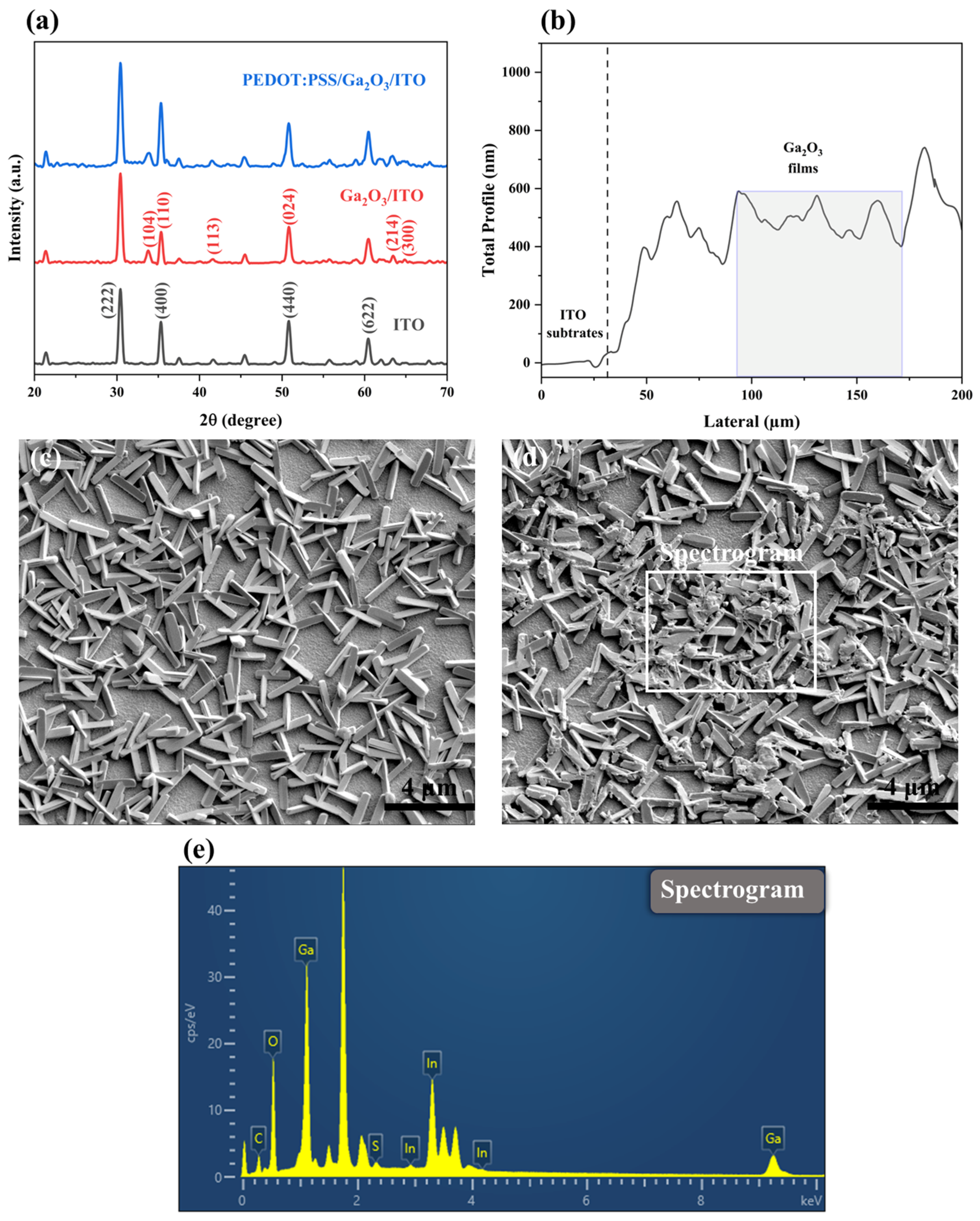
As shown in Figure 3a, the XRD pattern of the hydrothermally prepared film exhibits diffraction peaks that are in good agreement with the standard patterns of rhombohedral α-Ga2O3 (PDF#06-0503) and cubic In2O3 (PDF#06-0416). The peaks observed at 2θ values of 33.8°, 36.0°, 41.4°, 50.2°, 63.3°, and 64.7° are indexed to the (104), (110), (113), (024), (214), and (300) planes of α-Ga2O3, respectively. The additional peaks at 30.6°, 35.4°, 51.0°, and 60.7° originate from the (222), (400), (440), and (622) planes of the cubic In2O3 phase present in the ITO substrate. These assignments, based on the standard PDF cards, confirm that the as-prepared Ga2O3 film is single-phase α-Ga2O3. After the deposition of PEDOT:PSS, all characteristic diffraction peaks of α-Ga2O3 are fully retained without any peak shift or the appearance of additional reflections, indicating that the spin-coating process does not alter the crystal structure of Ga2O3 and that the amorphous PEDOT:PSS layer introduces no extra crystalline phases.
The thickness of the Ga2O3 film was characterized using a stylus profiler, and a representative profile is shown in Figure 3b. Averaging over the shaded region yields a mean thickness of 497 ± 87 nm, where the deviation reflects the intrinsic surface roughness and thickness undulation of the hydrothermally grown film.
Figure 3c shows a top-view SEM image of the bare α-Ga2O3 nanorods grown on the ITO substrate. The nanorods exhibit smooth surfaces and sharp edges, and are randomly distributed, mostly lying flat or inclined on the substrate. Statistical analysis of 30 randomly selected nanorods gives an average diameter of 338 ± 36 nm and an average length of 1770 ± 74 nm.
After PEDOT:PSS coating (Figure 3d), aggregates appear on most nanorod surfaces. EDS spectra from both the aggregated and flat regions were similar. The survey spectrum (Figure 3e) shows Ga and O peaks from α-Ga2O3, C and S signals confirming PEDOT:PSS, and In from the underlying ITO substrate. These results verify that PEDOT:PSS is successfully loaded onto the Ga2O3 nanorod film.
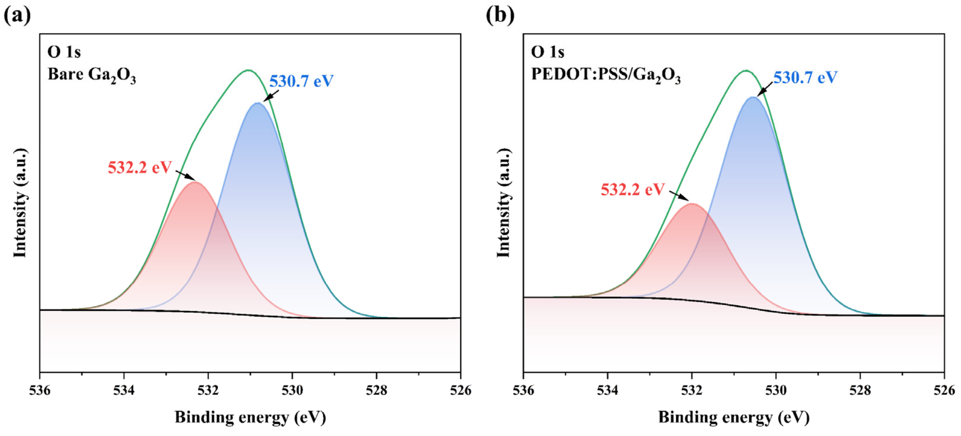
As shown in Figure 4, the XPS asymmetric O 1s peak can be divided into two subpeaks located at 530.7 and 532.2 eV by Gaussian fitting. The subpeak at the lower binding energy is assigned to metal-oxide Ga-O bonds, while the peak at higher binding energy originates from residual hydroxide groups coupled with oxygen vacancies [28,29]. After PEDOT:PSS coating, the relative area of the Ga-O peak increases from 59.2% to 68.5%, while that of the defect-related peak decreases from 40.8% to 31.5%. It is worth noting that the sulfonate groups of PSS also contribute an O 1s signal in the 531.5–532.5 eV region [30]. Therefore, the defect-peak area obtained for the heterostructure represents an upper bound. This clear reduction in the defect-related O 1s component indicates that PEDOT:PSS effectively passivates the oxygen-vacancy defects on the Ga2O3 surface.

3.2. Spin-Speed-Dependent Properties of PEDOT:PSS Films

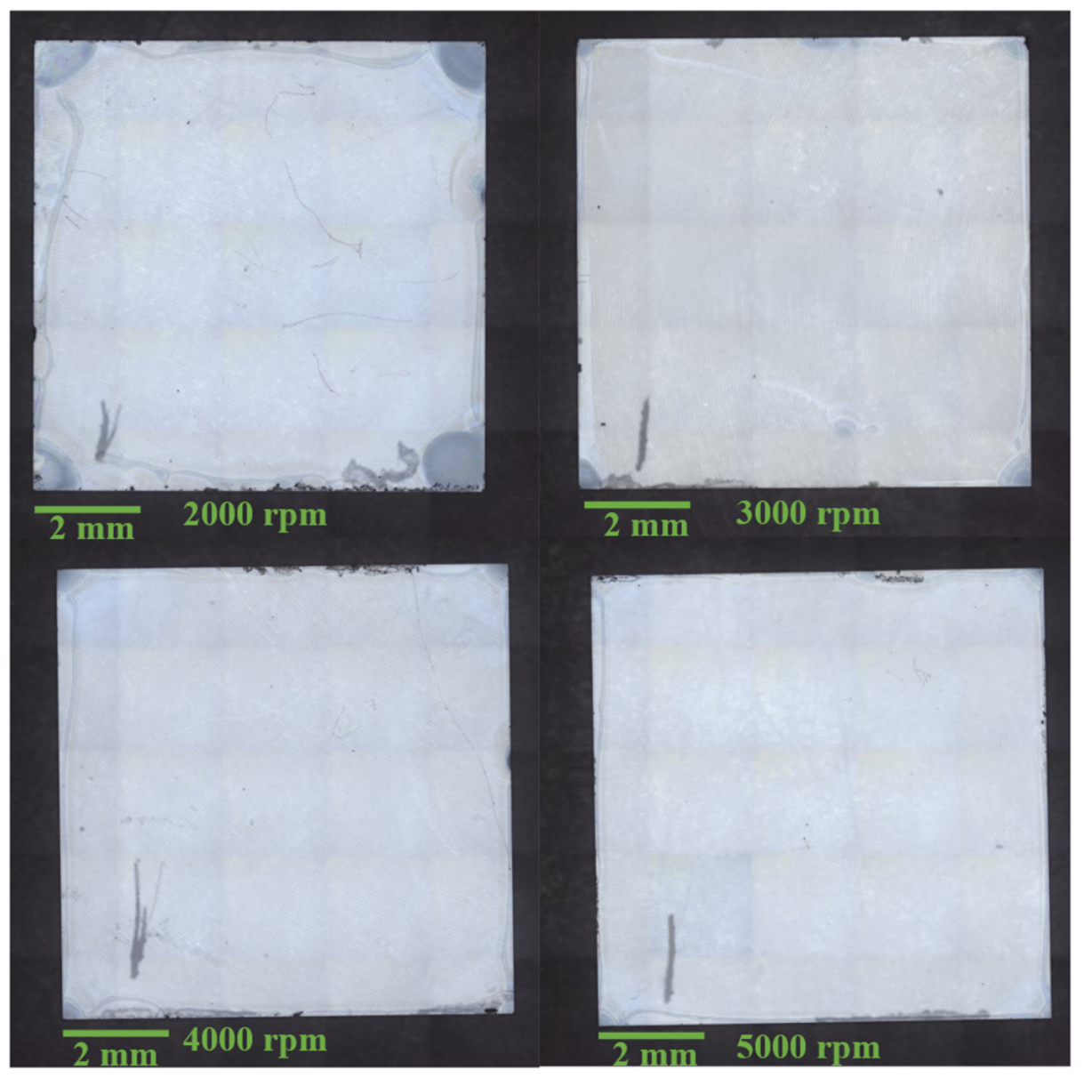
The LCSM characterization results of the PEDOT:PSS thin films are presented in Figure 5. During spin-coating, a typical edge bead effect was observed at the substrate edge due to solvent residues and thickness protrusions, which is an inherent edge effect jointly induced by centrifugal force, surface tension, and hydrodynamics [31]. With the increase in spin-coating speed, the centrifugal force is significantly enhanced, promoting sufficient detachment of the solvent at the edge, which remarkably weakens the edge bead effect, substantially reduces solvent residues, and gradually improves the surface uniformity of the PEDOT:PSS thin film.
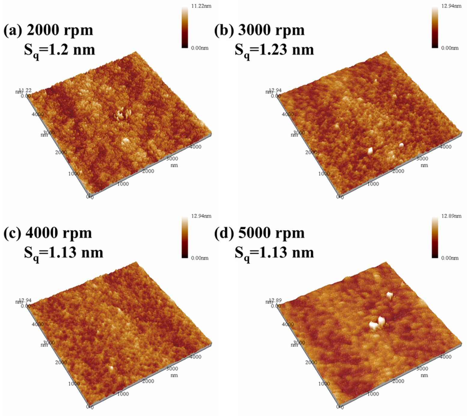
Figure 6 displays the three-dimensional AFM morphologies of the PEDOT:PSS films. All samples were scanned over an area of 5 × 5 μm. The root-mean-square roughness (Sq) shows a slight but systematic trend with spin speed: from 1.20 nm (2000 rpm) and 1.23 nm (3000 rpm) to 1.13 nm (4000 rpm) and 1.13 nm (5000 rpm). This mild decrease suggests that higher spin speeds favor a marginally smoother surface, likely due to more efficient removal of solvent and a reduced edge-bead effect, leading to improved film planarity. Despite this trend, all Sq values remain below 1.3 nm, confirming atomically ultra-smooth surfaces that provide excellent contact quality for the heterojunction interface.
The thickness of the PEDOT:PSS films was determined by X-ray reflectivity (XRR) measurements. The XRR curves were fitted using a Parratt recursive model to simultaneously extract the film thickness and density. As shown in Table 1, with increasing spin speed, the film thickness decreases monotonically from 44.18 nm to 33.27 nm, following the conventional behavior of spin coating. More notably, the XRR-derived film density also exhibits a monotonic decline from 1.84 g/cm3 to 1.75 g/cm3. This trend suggests a progressively looser molecular packing at higher spin speeds, which is consistent with the incomplete percolation network inferred for the thinnest films (Section 3.5).
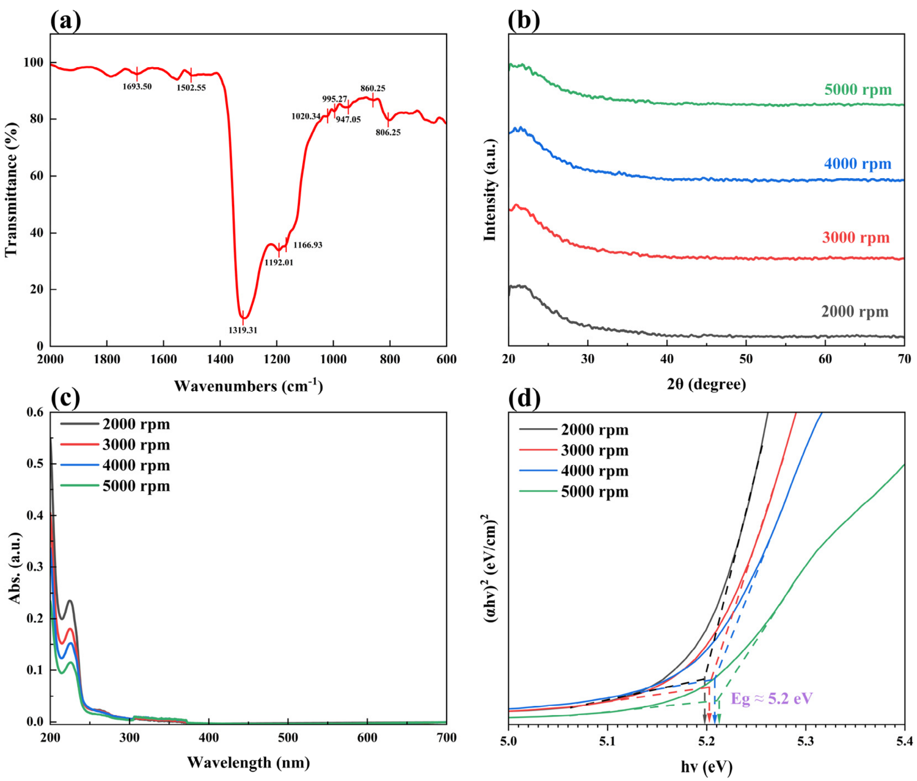
The full FTIR spectrum was recorded over the range of 400–4000 cm−1. Figure 7a shows the fingerprint region (600–2000 cm−1) where all characteristic vibrational modes of PEDOT:PSS are concentrated. The vibration at 1693.50 cm−1 is assigned to the C=C stretching vibration. The absorption band at 1192.08 cm−1 is attributed to the SO3H group of PSS. The peaks at 1502.55 cm−1 and 1319.31 cm−1 correspond to the C=C and C-C stretching vibrations in the thiophene ring of PEDOT, respectively. The absorption band in the range of approximately 840–1000 cm−1 originates from the C-S stretching vibration in the quinoid structure of the thiophene ring. The peaks between 1000 and 1200 cm−1 can be tentatively assigned to the ethylenedioxy group.
Figure 7b displays the X-ray diffraction (XRD) patterns of single-layer PEDOT:PSS thin films prepared at different spin-coating speeds, with all films grown on quartz glass substrates. Except for a broad diffraction peak near 20° (attributed to the quartz substrate), no obvious diffraction peaks are observed. This result indicates that the PEDOT:PSS thin films annealed at 150 °C for 15 min are amorphous.
Figure 7c presents the UV-vis absorption spectra of the PEDOT:PSS films. The films exhibit high transparency in the visible region but show non-negligible absorption in the solar-blind UV region. As the spin-coating speed increases, the absorbance in the solar-blind UV region decreases accordingly.
The transmittance (T) of PEDOT:PSS at 267 nm was calculated using the Beer-Lambert Equation (1):
T = 10 A
where A is the absorbance. The transmittance at 267 nm decreases from approximately 97.03% to 95.24% as the film thickness increases from 33.27 nm to 44.18 nm. This indicates that a thicker PEDOT:PSS layer induces stronger parasitic solar-blind UV absorption, thereby reducing the photon flux reaching the Ga2O3 absorption layer.
The corresponding optical band gap can be estimated by the Tauc Equation (2):
α h v n = A h v E g
where α is the optical absorption coefficient, hv is the photon energy ( h is Planck’s constant, v is the frequency), E g is the optical band gap, A is a constant, and n is determined by the transition type. For PEDOT:PSS, n = 2 (corresponding to direct allowed transition). As shown in Figure 7d, the optical absorption edge of the PEDOT:PSS films was analyzed using the Tauc method with the proper extrapolation (PE) technique [32,33]. The extracted effective optical band gap values lie within a narrow range centered around ~5.2 eV across all four spin-coating speeds. This indicates that the fundamental electronic structure of PEDOT:PSS is essentially independent of the film thickness, and the observed variation falls within the uncertainty of the graphical extrapolation method.

3.3. Energy-Level Alignment and Carrier-Transfer Mechanism

To understand the separation process of photogenerated electron–hole pairs in the device, it is necessary to determine the conduction band (CB) and valence band (VB) potentials of each component. These energy levels are calculated by the following empirical Equations (3) and (4):
E CB = χ E e E g / 2
E VB = E CB + E g
where E CB and E VB represent the conduction band and valence band potentials, respectively, and E g is the optical band gap of the semiconductor. In addition, E e denotes the energy difference in free electrons relative to hydrogen atoms (4.5 eV) [34]. Finally, χ represents the electronegativity of the semiconductor, which is calculated by the following Equation (5):
χ = [ ( χ A a χ B b ] 1 / a + b
where a and b are the number of atoms in the compound, respectively [35]. The electronegativities of Ga and O are 3.20 eV and 7.54 eV, respectively [36]. Therefore, the electronegativity of Ga2O3 can be calculated as 5.35 eV. Under the experimental conditions, the optical band gap E g of Ga2O3 is 5.06 eV [27]. Further calculations show that VB potential and CB potential positions of Ga2O3 relative to the normal hydrogen electrode (NHE) are 3.38 eV and −1.68 eV, respectively. The lowest unoccupied molecular orbital (LUMO) and highest occupied molecular orbital (HOMO) positions of PEDOT:PSS relative to NHE are −1.5 eV and 0.7 eV, respectively [37].
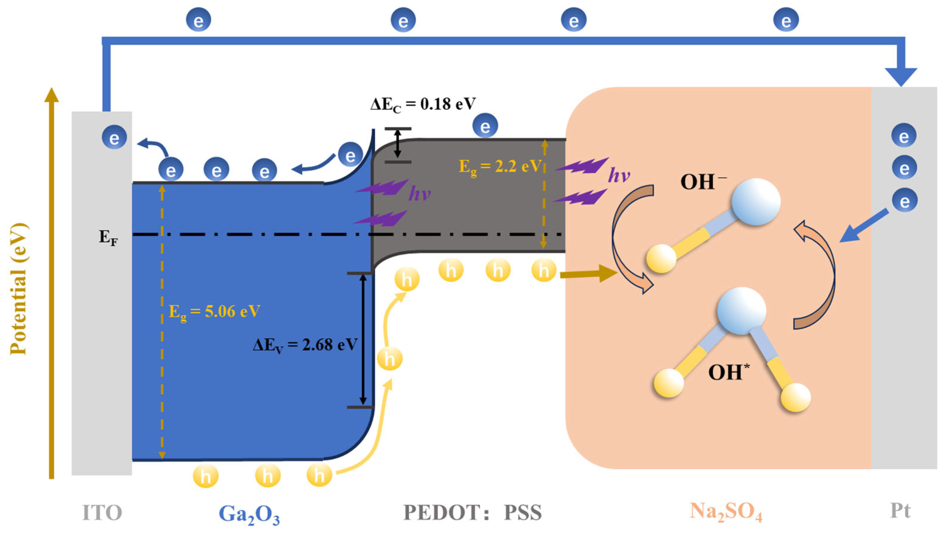
When PEDOT:PSS is in contact with Ga2O3, a heterojunction is formed with a valence band offset Δ E V of 2.68 eV and a conduction band offset Δ E C of 0.18 eV. As shown in Figure 8, to maintain the Fermi level equilibrium, the energy bands of p-type PEDOT:PSS shift upward and bend downward at the interface, while those of n-type Ga2O3 shift downward and bend upward. Consequently, a space charge region is formed on both sides of the interface, and a built-in electric field is established.
Under solar-blind UV illumination, incident photons pass through the semitransparent PEDOT:PSS layer before being absorbed by Ga2O3. Because PEDOT:PSS exhibits non-negligible absorption in the 200–280 nm range, an excessively thick PEDOT:PSS film attenuates the photon flux that reaches the Ga2O3 active region, thereby reducing the photon utilization efficiency η t r .
The absorption coefficient of Ga2O3 at 267 nm is estimated to be approximately 2.5 × 104 cm−1 [38,39,40], corresponding to a penetration depth (1/α) of about 400 nm. Since the average thickness of the Ga2O3 film is ∼497 nm, the majority of photons are absorbed in the near interface region, and photogenerated carriers are predominantly created in the vicinity of the heterojunction. The built in field subsequently drives electrons toward the ITO electrode and extracts holes toward the PEDOT:PSS/electrolyte interface.
For a bare Ga2O3 film, the high density of surface defects captures photogenerated carriers rapidly, causing severe surface recombination and therefore a weak photocurrent. In the PEDOT:PSS/Ga2O3 heterojunction, however, the strong built in field greatly facilitates charge separation. Holes are swiftly extracted by PEDOT:PSS, facilitated by the large valence band offset ( Δ E V = 2.68   eV ), and participate in the oxidation reaction at the semiconductor/electrolyte interface (h+ + OH → OH*). Simultaneously, photogenerated electrons drift toward the Ga2O3/ITO contact. Although a small conduction band offset ( Δ E C = 0.18   eV ) exists, it is small enough to allow efficient electron transfer via tunneling and thermionic emission, enabling collection by the ITO anode. From there, electrons travel through the external circuit to the Pt counter electrode and drive the reduction reaction (e + OH* → OH), completing the current loop. The entire process proceeds without any external bias, endowing the PEDOT:PSS/Ga2O3 heterojunction PEC detector with self-powered operation.
It is worth noting that the Ga2O3/ITO interface, although not a deliberately engineered junction in this work, warrants a brief discussion. Due to the work function mismatch between ITO and α-Ga2O3, a Schottky barrier could in principle form at this interface. However, two factors render the contact essentially Ohmic. First, ITO is degenerately doped with a carrier concentration of ~1020 cm−3, which creates an ultrathin space-charge region that allows efficient electron tunneling. Second, the low-temperature hydrothermal growth introduces a high density of interface states, which can pin the Fermi level and effectively reduce the barrier height. Experimentally, the bare Ga2O3 device delivers a measurable photocurrent under zero bias (Figure 9), confirming that photogenerated electrons are efficiently collected by the ITO electrode. Therefore, the Ga2O3/ITO interface is not the performance-limiting junction in our device; the charge separation and self-powered operation are predominantly governed by the PEDOT:PSS/Ga2O3 heterojunction.
Consequently, the overall device performance is governed by the product of three efficiencies as shown in Equation (6):
R d e v i c e   η p h o t o · η s e p · η t r
where η s e p is primarily determined by the energy-band alignment and interfacial quality of the heterojunction and, once a complete PEDOT:PSS coating is formed, shows little dependence on the organic film thickness. As for η p h o t o , the transmittance of all PEDOT:PSS films at the operating wavelength of 267 nm exceeds 95% (Figure 7c), meaning the variation in parasitic absorption across the thickness range is marginal. Therefore, the non-monotonic thickness dependence observed in this work originates predominantly from the competition between conductive network continuity and out-of-plane transport barrier within η t r ; the optimal device performance is attained at the thickness where these two factors are best balanced.

3.4. Self-Powered Photoresponse and Thickness-Dependent Optimization

All device performances were characterized in 0.1 M Na2SO4 electrolyte using a three-electrode configuration. The current density (J), responsivity (R), and specific detectivity (D*) were calculated by the following Equations (7)–(9):
J = ( I λ I d ) / S
R = ( I λ I d ) / P λ S
D * = R S / 2 e I d
where I λ is the photocurrent, I d is the dark current, S is the effective illumination area (0.5 cm2), P λ is the light intensity, and e is the electron charge.
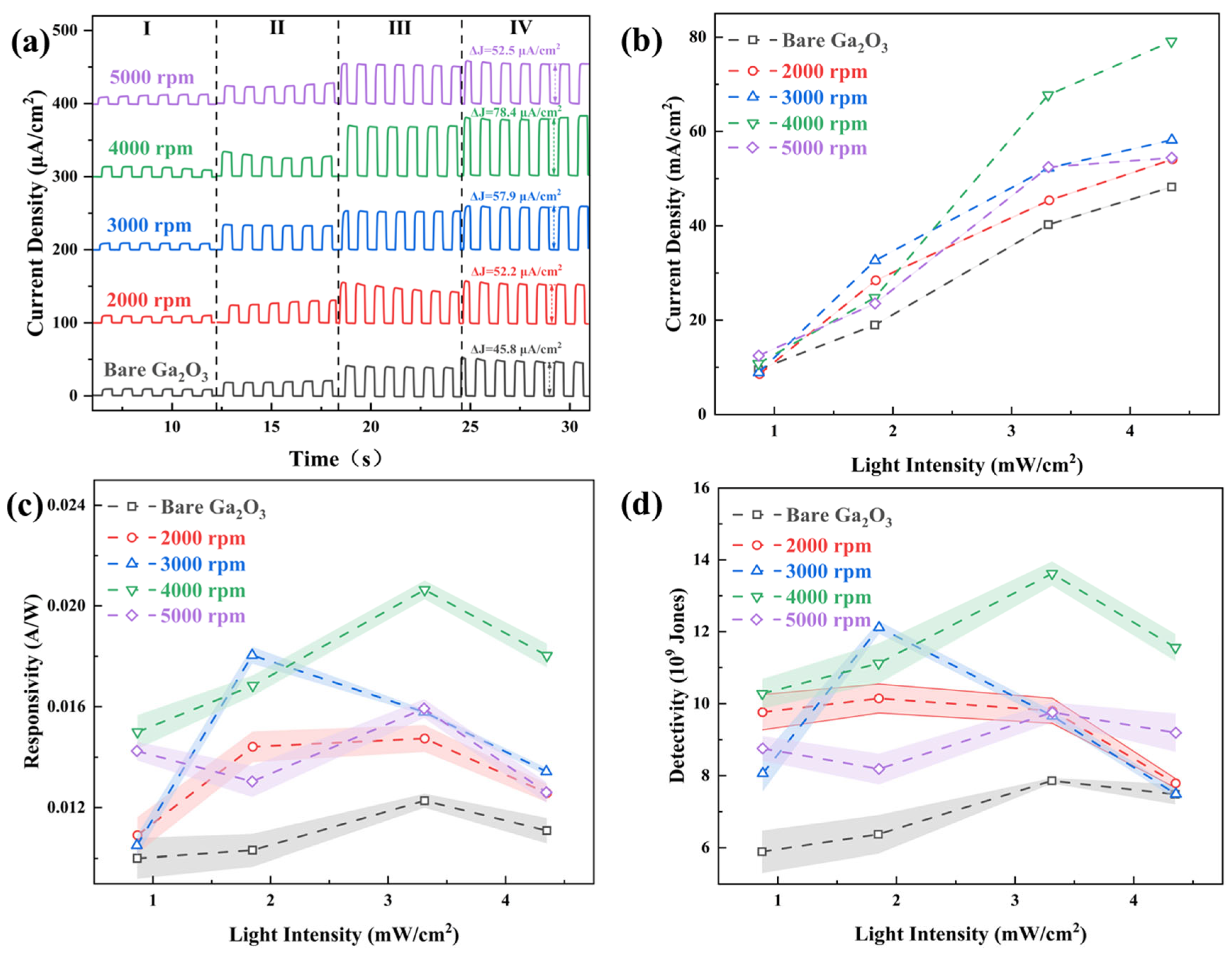
Figure 9a,b show the transient photocurrent responses of the devices under periodic on/off switching (1 s interval, 50% duty cycle) of 267 nm UV light with four different optical irradiances (I-IV: 0.866, 1.847, 3.310, and 4.350 mW/cm2, respectively). The photocurrent density of each device increases monotonically with the irradiance. All PEDOT:PSS/Ga2O3 devices produce significantly higher photocurrent densities than the bare Ga2O3 reference, and the device fabricated at 4000 rpm delivers the largest value of 78.4 μA/cm2 under the maximum irradiance of 4.350 mW/cm2.
As shown in Figure 9c,d the responsivity and specific detectivity of all PEDOT:PSS/Ga2O3 devices are much higher than those of the bare Ga2O3 device. Both parameters initially increase and then slightly decrease with increasing light intensity. The 4000 rpm device (36.50 nm) achieves peak values of R = 20.6 mA/W and D* = 1.36 × 10¹⁰ Jones at an irradiance of 3.310 mW/cm2. The slight decrease in responsivity at higher intensities can be attributed to enhanced electron–hole recombination in the nanorods under higher carrier densities.
The photoresponse varies non monotonically with PEDOT:PSS thickness, peaking at an intermediate value and thereby confirming the trade-off inherent in thickness regulation. At 5000 rpm, the film thickness decreases to 33.27 nm, which falls within the percolation transition region (typically about 30 nm) recognized for spin-coated PEDOT:PSS films [25]. In this regime, a fully dense and continuous conductive network has not yet been established, significantly reducing the hole extraction and transport efficiency η t r . The density trend obtained from XRR fitting (Table 1) is consistent with this incomplete connectivity: a monotonic decrease in film density from 1.84 to 1.75 g/cm3 indicates progressively looser molecular packing, which further impairs the formation of a continuous percolation network and thus degrades η t r .
By contrast, the films with thicknesses of 44.18 and 42.66 nm are well above the critical percolation threshold and form stable, continuous conductive networks. However, these thicker films exhibit diminished photoresponse. This can be understood from the layered microstructure of PEDOT:PSS. As proposed by Nardes et al. [26], spin-coated PEDOT:PSS comprises alternating PEDOT-rich conductive layers and insulating PSS lamellae, with one complete “PEDOT + PSS” period of approximately 6 nm. Given that the 36.50 nm film already establishes a continuous percolation network, any additional thickness mainly introduces extra PSS lamellae. These insulating lamellae act as barriers to out-of-plane hole transport, thereby reducing the effective hole extraction efficiency η t r . Consequently, the optimal device performance is realized at an intermediate thickness that balances conductive network continuity against the accumulation of vertical transport barriers.

3.5. Electrochemical Impedance Spectroscopy

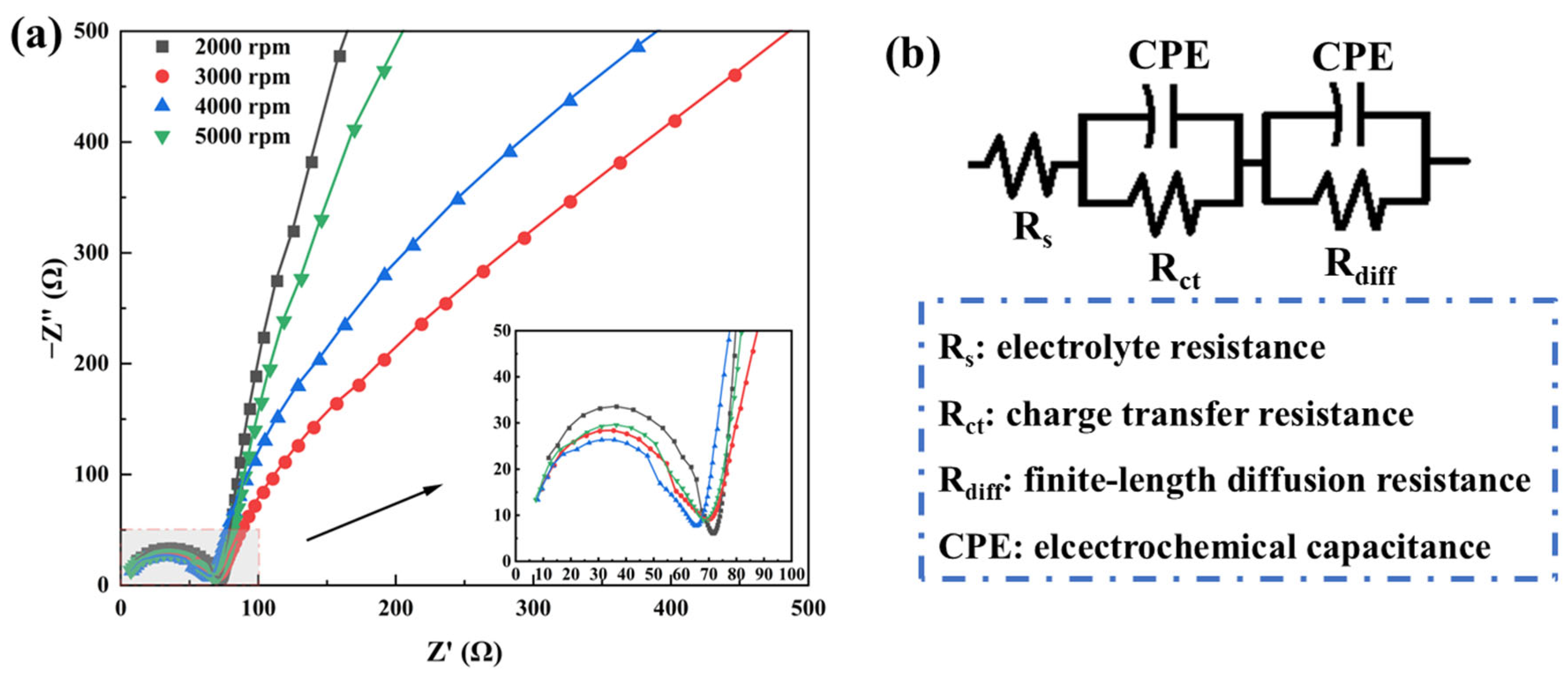
To further verify the thickness-dependent hole-transfer mechanism proposed in Section 3.4, electrochemical impedance spectroscopy (EIS) measurements were performed on all PEDOT:PSS/Ga2O3 devices at 0 V vs. Ag/AgCl in the dark. Figure 10a shows the Nyquist impedance plots of the devices with different PEDOT:PSS thicknesses, and Figure 10b presents the equivalent circuit used for fitting, with the extracted parameters summarized in Table 2.
The high-frequency semicircle in the Nyquist plots is attributed to the charge-transfer resistance Rct at the PEDOT:PSS/electrolyte interface [41]. The variation of Rct across the four devices is generally consistent with the photoresponse trend observed in Figure 9. Given that interfacial charge transfer is the rate-limiting step for hole collection in the PEC configuration, the observed changes in Rct, though modest in magnitude, are sufficient to account for the corresponding variation in η t r .
The Rct effectively integrates the two competing transport factors examined in this work. When the PEDOT:PSS film is too thin, the incomplete percolation network restricts the effective interfacial area available for hole transfer, leading to a larger Rct. When the film is too thick, additional insulating PSS lamellae create a higher kinetic barrier for hole extraction, which similarly increases Rct. The lowest Rct is therefore observed at the intermediate thickness of 36.50 nm, where percolation continuity and the accumulation of insulating PSS lamellae are optimally balanced, yielding the highest η t r .

3.6. Spectral Selectivity, Response Speed, and Storage Stability

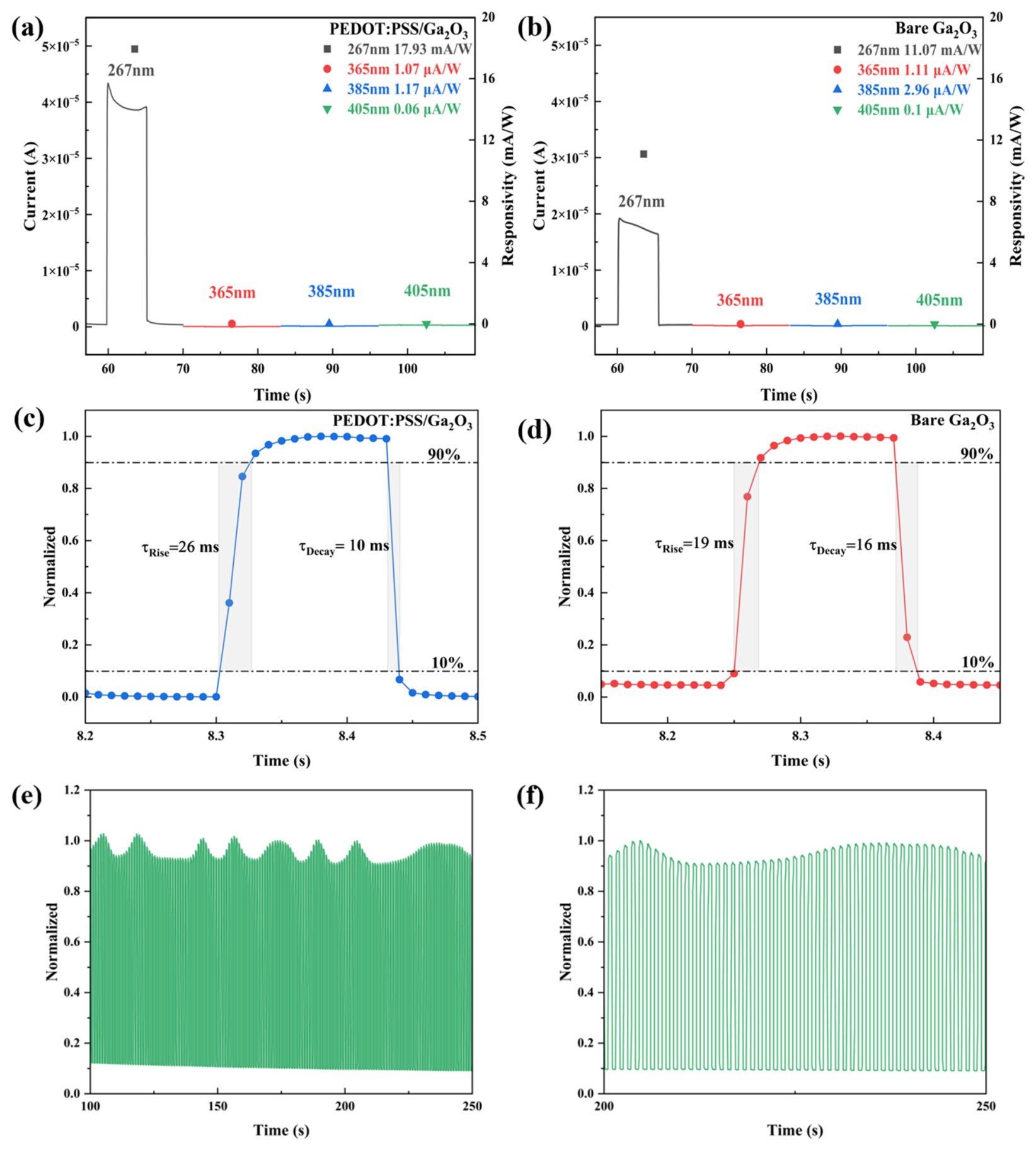
Figure 11a,b compare the spectral selectivity of the optimized PEDOT:PSS/Ga2O3 device and the bare Ga2O3 device. The PEDOT:PSS/Ga2O3 device exhibits a UV/visible rejection ratio R267/R405 as high as 3.18 × 10⁵, and the R267/R365 reaches 1.67 × 10⁴. In contrast, the bare Ga2O3 device shows values of only 1.12 × 10⁵ and 1.00 × 10⁴, respectively. This significant enhancement is attributed to the surface passivation effect of PEDOT:PSS, which reduces surface oxygen vacancies and defect states in Ga2O3, thereby suppressing the band-tail absorption of 365 nm near-UV light and resulting in purer solar-blind characteristics.
Response time was evaluated under 267 nm illumination (intensity IV). The rise time ( τ r i s e , 10–90%) and decay time ( τ d e c a y , 90–10%) of the PEDOT:PSS/Ga2O3 device are 26 ms and 10 ms, respectively, while those of the bare Ga2O3 device are 19 ms and 16 ms (Figure 11c,d). The slightly longer τ r i s e (26 ms vs. 19 ms) can be explained by the additional RC time constant introduced by the limited hole injection rate at the PEDOT:PSS/electrolyte and organic–inorganic interfaces. The clearly shorter τ d e c a y (10 ms vs. 16 ms) reflects the efficient hole extraction capability of PEDOT:PSS, which prevents the accumulation of photogenerated carriers on the Ga2O3 surface and suppresses the slow trap-assisted recombination process that dominates the decay of the bare device.
The stability of the PEDOT:PSS/Ga2O3 device was examined by cycling under 267 nm light (intensity IV) after storage in ambient air for 2 months. Figure 11e shows 150 consecutive on-off cycles (from 100 to 250 s) with normalized current, demonstrating good operational repeatability and environmental storage stability. A magnified view of the 200–250 s cycles is shown in Figure 11f.
The performance of our device is compared with representative Ga2O3-based self-powered solar-blind photodetectors in Table 3. These benchmarks span various strategies, including elemental doping, inorganic heterojunctions, and organic–inorganic hybrid structures. The present PEDOT:PSS/α-Ga2O3 device delivers a competitive responsivity of 20.6 mA/W and fast rise/decay times of 26/10 ms at zero bias. While several devices in the table exhibit higher responsivity or detectivity, they often rely on high-temperature epitaxy, vacuum deposition, or complex multilayer engineering. The approach demonstrated here is distinct in that it combines a low-temperature hydrothermal process with a simple spin-coated organic layer, achieving a favorable balance between performance and fabrication simplicity through thickness-controlled interface engineering.

4. Conclusions

In summary, a self-powered PEC solar-blind ultraviolet photodetector was constructed using a PEDOT:PSS/Ga2O3 organic–inorganic heterojunction. The PEDOT:PSS layer simultaneously acts as a hole transport layer and an interface passivation layer. The heterojunction provides efficient charge separation η s e p . The photoresponse shows a non-monotonic thickness dependence governed mainly by the trade-off between conductive network continuity and out-of-plane transport barrier within the hole transport efficiency η t r , with parasitic absorption playing only a minor role. The device optimized at 4000 rpm (36.50 nm) achieves the best balance, yielding a responsivity of 20.6 mA/W and a detectivity of 1.36 × 10¹⁰ Jones at 267 nm under zero bias, along with an R267/R405 of 3.18 × 10⁵ and fast 26/10 ms rise/decay times. This work highlights a balance-oriented hole transport engineering strategy that avoids the complexity of doping or high-vacuum processes, offering a practical route for low-cost, high-performance self-powered Ga2O3 based solar-blind photodetectors.

Author Contributions

Conceptualization, J.X. and R.Y.; data curation, J.X.; methodology, H.C.; formal analysis, J.X.; validation, J.X., H.C. and H.N.; investigation, C.Y. and H.Z.; resources, H.N.; writing—original draft preparation, J.X.; writing—review and editing, R.Y., H.N. and W.X.; visualization, J.X.; supervision, X.Z. and X.L.; project administration, J.P.; funding acquisition, H.N., R.Y. and D.L. All authors have read and agreed to the published version of the manuscript.

Funding

This research was funded by National Key R&D Program of China (Grant No. 2024YFB3614400), National Natural Science Foundation of China (Grant No. 62375057), Guangdong S&T Program (Grant No. 2024B0101040006), Guangzhou Science and Technology Plan (Grant No. 2025B01J4004), the Opening Project of Science and Technology on Reliability Physics and Application Technology of Electronic Component Laboratory (25D05), Guangdong Natural Science Foundation (No. 2024A1515012216 and 2026A1515012681), the Open Foundation of the Guangdong Provincial Key Laboratory of Electronic Information Products Reliability Technology (GDDZXX202504) and State Key Lab of Luminescent Materials and Devices (Skllmd-2024-05 and Skllmd-2025-07).

Institutional Review Board Statement

Not applicable.

Informed Consent Statement

Not applicable.

Data Availability Statement

The data are contained within the article.

Acknowledgments

We thank all the participants, institutions, editors, and reviewers for enabling us to conduct this research.

Conflicts of Interest

Authors Haitao Zhu, Xu Zhou and Xiaojie Li were employed by the company Shenzhen Yaham Optoelectronics Co., Ltd. The remaining authors declare that the research was conducted in the absence of any commercial or financial relationships that could be construed as potential conflicts of interest.

References

  1. Su, L.X.; Yang, W.; Cai, J.; Chen, H.Y.; Fang, X.S. Self-Powered Ultraviolet Photodetectors Driven by Built-In Electric Field. Small 2017, 13, 1701687. [Google Scholar] [CrossRef] [PubMed]
  2. Xu, H.; Weng, Y.; Chen, K.; Wu, C.; Hu, H.; Guo, D. Ultra-Low BER Encrypted Communication Based on Self-Powered Bipolar Photoresponse Ultraviolet Photodetector. Adv. Opt. Mater. 2025, 13, 2402238. [Google Scholar] [CrossRef]
  3. Varshney, U.; Aggarwal, N.; Gupta, G. Current advances in solar-blind photodetection technology: Using Ga2O3 and AlGaN. J. Mater. Chem. C 2022, 10, 1573−1593. [Google Scholar] [CrossRef]
  4. Peng, Z.; Hou, X.; Han, Z.; Gan, Z.; Li, C.; Wu, F.; Bai, S.; Yu, S.; Liu, Y.; Yang, K.; et al. Ga2O3 Photon-Controlled Diode for Sensitive DUV/X-Ray Detection and High-Resolution Array Imaging Application. Adv. Funct. Mater. 2024, 34, 2405277. [Google Scholar] [CrossRef]
  5. Boruah, B.D. Zinc oxide ultraviolet photodetectors: Rapid progress from conventional to self-powered photodetectors. Nanoscale Adv. 2019, 1, 2059–2085. [Google Scholar] [CrossRef] [PubMed]
  6. Suchikova, Y.; Nazarovets, S.; Popov, A.I. Ga2O3 solar-blind photodetectors: From civilian applications to missile detection and research agenda. Opt. Mater. 2024, 157, 116397. [Google Scholar] [CrossRef]
  7. Lin, H.; Jiang, A.; Xing, S.; Li, L.; Cheng, W.; Li, J.; Miao, W.; Zhou, X.; Tian, L. Advances in Self-Powered Ultraviolet Photodetectors Based on P-N Heterojunction Low-Dimensional Nanostructures. Nanomaterials 2022, 12, 910. [Google Scholar] [CrossRef] [PubMed]
  8. Goel, V.; Kumar, Y.; Rawat, G.; Kumar, H. Self-powered photodetectors: A device engineering perspective. Nanoscale 2024, 16, 9235–9258. [Google Scholar] [CrossRef] [PubMed]
  9. Ahsan, U.; Elahi, E.; Sattar, A.; Sarkar, K.J.; Asad, M.; Mustafa, H.; Irfan, M.; Sabar, M.A.; Sofer, Z. Advances in visible and ultraviolet self-powered photodetectors: Exploring 2D materials and Janus heterostructures. Nanoscale 2026, 18, 537–574. [Google Scholar] [CrossRef] [PubMed]
  10. Shi, C.; Lv, Q.; Ren, R.; Xiong, W.; Wang, Z.; Yin, Y.; Liu, J. Challenges and opportunities in Ga2O3 solar-blind photodetectors: From material engineering to device realization. Mater. Sci. Semicond. Process. 2026, 208, 110547. [Google Scholar] [CrossRef]
  11. Xu, Y.; Cheng, Y.; Li, Z.; Feng, Q.; Zhang, Y.; Chen, D.; Zhu, W.; Zhang, J.; Zhang, C.; Hao, Y. High performance gate tunable solar blind ultraviolet phototransistors based on amorphous Ga2O3 films grown by mist chemical vapor deposition. Nano Sel. 2021, 2, 2112–2120. [Google Scholar] [CrossRef]
  12. Lu, Y.; Zou, X.; Krishna, S.; Tang, X.; Liu, Z.; Nong, M.; Liao, C.-H.; Yuvaraja, S.; Hassine, M.B.; Fariborzi, H.; et al. Thermal mismatch engineering induced freestanding and ultrathin Ga2O3 membrane for vertical electronics. Mater. Today Phys. 2023, 36, 101181. [Google Scholar] [CrossRef]
  13. Chiang, J.-L.; Yadlapalli, B.K.; Chen, M.-I.; Wuu, D.-S. A Review on Gallium Oxide Materials from Solution Processes. Nanomater. 2022, 12, 3601. [Google Scholar] [CrossRef] [PubMed]
  14. Tian, W.; Wang, Y.; Chen, L.; Li, L. Self-Powered Nanoscale Photodetectors. Small 2017, 13, 1701848. [Google Scholar] [CrossRef] [PubMed]
  15. Zhao, B.; Wang, F.; Chen, H.; Zheng, L.; Su, L.; Zhao, D.; Fang, X. An Ultrahigh Responsivity (9.7 mA W−1) Self-Powered Solar-Blind Photodetector Based on Individual ZnO-Ga2O3 Heterostructures. Adv. Funct. Mater. 2017, 27, 1700264. [Google Scholar] [CrossRef]
  16. An, Y.; Zhi, Y.; Wu, Z.; Cui, W.; Zhao, X.; Guo, D.; Li, P.; Tang, W. Deep ultraviolet photodetectors based on p-Si/i-SiC/n-Ga2O3 heterojunction by inserting thin SiC barrier layer. Appl. Phys. A 2016, 122, 1036. [Google Scholar] [CrossRef]
  17. Sun, X.Y.; Chen, X.H.; Hao, J.G.; Wang, Z.P.; Xu, Y.; Gong, H.H.; Zhang, Y.J.; Yu, X.X.; Zhang, C.D.; Ren, F.-F.; et al. A self-powered solar-blind photodetector based on polyaniline/α-Ga2O3 p−n heterojunction. Appl. Phys. Lett. 2021, 119, 141601. [Google Scholar] [CrossRef]
  18. Wang, Y.; Lin, Z.; Ma, J.; Wu, Y.; Yuan, H.; Cui, D.; Kang, M.; Guo, X.; Su, J.; Miao, J.; et al. Multifunctional solar-blind ultraviolet photodetectors based on p-PCDTBT/n-Ga2O3 heterojunction with high photoresponse. InfoMat 2024, 6, e12503. [Google Scholar] [CrossRef]
  19. Naponiello, G.; Venditti, I.; Zardetto, V.; Saccone, D.; Di Carlo, A.; Fratoddi, I.; Barolo, C.; Dini, D. Photoelectrochemical characterization of squaraine-sensitized nickel oxide cathodes deposited via screen-printing for p-type dye-sensitized solar cells. Appl. Surf. Sci. 2015, 356, 911–920. [Google Scholar] [CrossRef]
  20. Bonomo, M.; Naponiello, G.; Venditti, I.; Zardetto, V.; Di Carlo, A.; Dini, D. Electrochemical and Photoelectrochemical Properties of Screen-Printed Nickel Oxide Thin Films Obtained from Precursor Pastes with Different Compositions. J. Electrochem. Soc. 2017, 164, H137. [Google Scholar] [CrossRef]
  21. Al-Amiery, A.A.; Fayad, M.A.; Wahhab, H.A.A.; Al-Azzawi, W.K.; Mohammed, J.K.; Majdi, H.S. Interfacial Engineering for Advanced Functional Materials: Surfaces, Interfaces, and Applications. Results Eng. 2024, 22, 102125. [Google Scholar] [CrossRef]
  22. Venditti, I.; Barbero, N.; Russo, M.V.; Di Carlo, A.; Decker, F.; Fratoddi, I.; Barolo, C.; Dini, D. Electrodeposited ZnO with squaraine sentisizers as photoactive anode of DSCs. Mater. Res. Express 2014, 1, 015040. [Google Scholar] [CrossRef]
  23. Bedeloglu, A.; Demir, A.; Bozkurt, Y.; Sariciftci, N.S. A Photovoltaic Fiber Design for Smart Textiles. Text. Res. J. 2010, 80, 1065–1074. [Google Scholar] [CrossRef]
  24. Xiao, Z.; Chen, H.; Ning, H.; Luo, D.; Fang, X.; Li, M.; Su, G.; He, H.; Yao, R.; Peng, J. Self-Powered Ultraviolet Photodetectors Based on Conductive Polymers/Ga2O3 Heterojunctions: A Review. Polymers 2025, 17, 1384. [Google Scholar] [CrossRef] [PubMed]
  25. Nardes, A.M. On the Conductivity of PEDOT:PSS Thin Films. Ph.D. Thesis, Technische Universiteit Eindhoven, Eindhoven, The Netherlands, 2007. [Google Scholar] [CrossRef]
  26. Nardes, A.M.; Kemerink, M.; Janssen, R.A.J. Anisotropic hopping conduction in spin-coated PEDOT:PSS thin films. Phys. Rev. B 2007, 76, 085208. [Google Scholar] [CrossRef]
  27. Zhang, Y.; Chen, H.; Yao, R.; Su, G.; He, H.; Zheng, J.; Tang, H.; Lu, Y.; Ning, H.; Peng, J. High-Responsivity Self-Powered Photoelectrochemical Solar-Blind Ultraviolet Detector Based on (104)-Oriented Ga2O3 Nanorods. Surf. Interfaces 2025, 75, 107844. [Google Scholar] [CrossRef]
  28. He, F.; Wang, Y.; Lin, Z.; Su, J.; Zhang, J.; Chang, J.; Hao, Y. Aqueous solution-deposited aluminum-gallium-oxide alloy gate dielectrics for low voltage fully oxide thin film transistors. Appl. Phys. Lett. 2021, 119, 112102. [Google Scholar] [CrossRef]
  29. He, F.; Qin, Y.; Wan, L.; Su, J.; Lin, Z.; Zhang, J.; Chang, J.; Wu, J.; Hao, Y. Metal oxide heterojunctions for high performance solution grown oxide thin film transistors. Appl. Surf. Sci. 2020, 527, 146774. [Google Scholar] [CrossRef]
  30. Greczynski, G.; Kugler, T.; Salaneck, W.R. Characterization of the PEDOT-PSS system by means of X-ray and ultraviolet photoelectron spectroscopy. Thin Solid Films 1999, 354, 129–135. [Google Scholar] [CrossRef]
  31. Mahmoodi, S.; Weidner, D.E. Reduction in edge beading defects using two-axis spin coating technology: An analytical, numerical, and experimental study. J. Coat. Technol. Res. 2023, 20, 1759–1771. [Google Scholar]
  32. Brik, M.G.; Srivastava, A.M.; Popov, A.I. A few common misconceptions in the interpretation of experimental spectroscopic data. Opt. Mater. 2022, 127, 112276. [Google Scholar] [CrossRef]
  33. Jubu, P.R.; Yam, F.K.; Igba, V.M.; Beh, K.P. Tauc-plot scale and extrapolation effect on bandgap estimation from UV–vis–NIR data—A case study of β-Ga2O3. J. Solid State Chem. 2020, 290, 121576. [Google Scholar] [CrossRef]
  34. Schmickler, W.S. Roy Morrison: Electrochemistry at Semiconductor and Oxidized Metal Electrodes. Plenum Press, New York, London 1980. Berichte Der Bunsenges. Für Phys. Chem. 1981, 85, 621–622. [Google Scholar] [CrossRef]
  35. Yuan, Q.; Chen, L.; Xiong, M.; He, J.; Luo, S.L.; Au, C.T.; Yin, S.F. Cu2O/BiVO4 heterostructures: Synthesis and application in simultaneous photocatalytic oxidation of organic dyes and reduction of Cr (VI) under visible light. Chem. Eng. J. 2014, 255, 394–402. [Google Scholar] [CrossRef]
  36. Pearson, R.G. Absolute Electronegativity and Hardness: Application to Inorganic Chemistry. Inorg. Chem. 1988, 27, 734–740. [Google Scholar] [CrossRef]
  37. Fan, X.; Stott, N.E.; Zeng, J.; Li, Y.; Ouyang, J.; Chu, L.; Song, W. PEDOT:PSS materials for optoelectronics, thermoelectrics, and flexible and stretchable electronics. J. Mater. Chem. A 2023, 11, 18561. [Google Scholar] [CrossRef]
  38. Penman, L.T.; Johnston, Z.M.; Edwards, P.R.; Oshima, Y.; McAleese, C.; Mazzolini, P.; Bosi, M.; Seravalli, L.; Fornari, R.; Martin, R.W.; et al. Comparative Study of the Optical Properties of α-, β-, and κ-Ga2O3. Phys. Status Solidi B 2025, 262, 2400615. [Google Scholar] [CrossRef]
  39. Nicol, D.; Reynolds, S.; Barr, K.; Roberts, J.W.; Jarman, J.J.; Chalker, P.R.; Massabuau, F.C.-P. Constant Photocurrent Method to Probe the Sub-Bandgap Absorption in Wide Bandgap Semiconductor Films: The Case of α-Ga2O3. Phys. Status Solidi B 2024, 261, 2300470. [Google Scholar] [CrossRef]
  40. Segura, A.; Artús, L.; Cuscó, R.; Goldhahn, R.; Feneberg, M. Band Gap of Corundumlike α-Ga2O3 Deter-mined by Absorption and Ellipsometry. Phys. Rev. Mater. 2017, 1, 024604. [Google Scholar] [CrossRef]
  41. Meher, S.K.; Justin, P.; Rao, G.R. Nanoscale morphology dependent pseudocapacitance of NiO: Influence of intercalating anions during synthesis. Nanoscale 2011, 3, 683–692. [Google Scholar] [CrossRef] [PubMed]
  42. Zhang, B.; Wu, H.; Feng, C.; Zhang, Z.; Yu, H.; Zhang, C.; Lin, S.; Xu, C.; Bai, H.; Guo, F. Self-Powered Solar-Blind Photodetectors Based on α-Ga2O3 Nanorod Arrays. ACS Appl. Nano Mater. 2022, 5, 11956–11963. [Google Scholar] [CrossRef]
  43. Guo, J.C.; Sun, G.W.; Fan, M.M.; Fu, X.C.; Yao, J.J.; Wang, Y.D. Hydrothermal Growth of an Al-Doped α-Ga2O3 Nanorod Array and Its Application in Self-Powered Solar-Blind UV Photodetection Based on a Photoelectrochemical Cell. Micromachines 2023, 14, 1336. [Google Scholar] [CrossRef] [PubMed]
  44. Zhou, X.; Ye, L.; Yuan, L.; Zhang, D.; Zhang, H.; Pang, D.; Tang, Y.; Li, H.; Li, W.; Zeng, H. Mg-Doped α-Ga2O3 Nanorods for the Construction of Photoelectrochemical-Type Self-Powered Solar Blind UV Photodetectors and Underwater Imaging Application. Adv. Sci. 2025, 12, 2413074. [Google Scholar] [CrossRef] [PubMed]
  45. Feng, S.; Liu, Z.; Feng, L.; Wang, J.; Xu, H.; Deng, L.; Zhou, O.; Jiang, X.; Liu, B.; Zhang, X. High-performance self-powered ultraviolet photodetector based on Ga2O3/GaN heterostructure for optical imaging. J. Alloys Compd. 2023, 945, 169274. [Google Scholar] [CrossRef]
  46. Li, S.; Yan, Z.; Liu, Z.; Chen, J.; Zhi, Y.; Guo, D.; Li, P.; Wu, Z.; Tang, W. A self-powered solar-blind photodetector with large Voc enhancing performance based on the PEDOT:PSS/Ga2O3 organic–inorganic hybrid heterojunction. J. Mater. Chem. C 2020, 8, 1292–1300. [Google Scholar] [CrossRef]
  47. Park, S.; Yoon, Y.; Kim, H.; Park, T.; Kim, K.; Hong, J. A Self-Powered High-Responsivity, Fast-Response-Speed Solar-Blind Ultraviolet Photodetector Based on CuO/β-Ga2O3 Heterojunction with Built-In Potential Control. Nanomaterials 2023, 13, 954. [Google Scholar] [CrossRef] [PubMed]
  48. Wu, D.; Zhao, Z.; Lu, W.; Rogée, L.; Zeng, L.; Lin, P.; Shi, Z.; Tian, Y.; Li, X.; Tsang, Y.H. Highly sensitive solar-blind deep ultraviolet photodetector based on graphene/PtSe2/β-Ga2O3 2D/3D Schottky junction with ultrafast speed. Nano Res. 2021, 14, 1973–1979. [Google Scholar] [CrossRef]
  49. Wang, H.; Chen, H.; Li, L.; Wang, Y.; Su, L.; Bian, W.; Li, B.; Fang, X. High Responsivity and High Rejection Ratio of Self-Powered Solar-Blind Ultraviolet Photodetector Based on PEDOT:PSS/β-Ga2O3 Organic/Inorganic p–n Junction. J. Phys. Chem. Lett. 2019, 10, 6850–6856. [Google Scholar] [CrossRef] [PubMed]
  50. Yan, Z.; Li, S.; Liu, Z.; Zhi, Y.; Dai, J.; Sun, X.; Sun, S.; Guo, D.; Wang, X.; Li, P.; et al. High sensitivity and fast response self-powered solar-blind ultraviolet photodetector with a β-Ga2O3/spiro-MeOTAD p-n heterojunction. J. Mater. Chem. C 2020, 8, 4502–4509. [Google Scholar] [CrossRef]
  51. Zhang, X.; Liu, N.; Lin, H.; Han, D.; Zhang, W.; Ye, J. Interface-Engineered High-Performance Self-Powered Solar-Blind Photodetector Based on NiO/ε-Ga2O3 Heterojunctions. ACS Appl. Mater. Interfaces 2025, 17, 17117–17126. [Google Scholar] [CrossRef] [PubMed]
  52. Guo, D.; Su, Y.; Shi, H.; Li, P.; Zhao, N.; Ye, J.; Wang, S.; Liu, A.; Chen, Z.; Li, C.; et al. Self-Powered Ultraviolet Photodetector with Superhigh Photoresponsivity (3.05 A/W) Based on the GaN/Sn:Ga2O3 pn Junction. ACS Nano 2018, 12, 12827–12835. [Google Scholar] [CrossRef] [PubMed]
Figure 1. Fabrication flow chart of the poly(3,4-ethylenedioxythiophene):polystyrene sulfonate (PEDOT:PSS)/Ga2O3 heterojunction device.
Inorganics 14 00209 g001
Figure 2. PEDOT:PSS/Ga2O3 UV photodetector (PD) devices: (a) Schematic illustration of the photoelectrochemical (PEC) measurement setup. (b) Photograph of the devices.
Inorganics 14 00209 g002
Figure 3. (a) XRD patterns of the bare Ga2O3 film and the PEDOT:PSS/Ga2O3 heterostructure on ITO substrates. (b) Thickness profile of the Ga2O3 film obtained by a stylus profiler; (c) surface SEM image of bare Ga2O3 nanorods; (d) surface SEM image after PEDOT:PSS coating; (e) EDS survey spectrum of the PEDOT:PSS/Ga2O3 heterostructure film.
Inorganics 14 00209 g003
Figure 4. XPS O 1s spectra of (a) bare Ga2O3 film and (b) PEDOT:PSS/Ga2O3 heterostructure.
Inorganics 14 00209 g004
Figure 5. LCSM images of the PEDOT:PSS thin films prepared with different spin-coating speed.
Inorganics 14 00209 g005
Figure 6. 3D AFM topography image of the PEDOT:PSS thin films prepared with different spin-coating speed: (a) 2000 rpm; (b) 3000 rpm; (c) 4000 rpm; (d) 5000 rpm.
Inorganics 14 00209 g006
Figure 7. PEDOT:PSS thin film: (a) FTIR spectrum; (b) XRD spectra; (c) UV-vis absorption spectra; (d) ( α hv ) 2 - hv curves.
Inorganics 14 00209 g007
Figure 8. Schematic diagram of energy bands and charge transfer process in PEDOT:PSS/Ga2O3 heterojunction.
Inorganics 14 00209 g008
Figure 9. Performance of PEDOT:PSS/Ga2O3 PEC UV PDs with various light intensities: (a) Transient responses. (b) Photocurrent density Jph. (c) Responsivity. (d) Detectivity. The shaded bands represent the standard deviation from three repeated measurements on the same device.
Inorganics 14 00209 g009
Figure 10. PEDOT:PSS/Ga2O3 PEC UV PDs: (a) Nyquist impedance plots; (b) equivalent circuit used for fitting.
Inorganics 14 00209 g010
Figure 11. PEDOT:PSS/Ga2O3 and bare Ga2O3 devices: (a,b) Spectral selectivity; (c,d) Response time; (e) Cycling stability of PEDOT:PSS/Ga2O3 UV PD; (f) Amplifying I-T curves in the range of 200–250 s.
Inorganics 14 00209 g011
Table 1. poly(3,4-ethylenedioxythiophene):polystyrene sulfonate (PEDOT:PSS) film density and thickness determined by XRR fitting.
Spin-Coating Speed (rpm)Fitting Density (g/cm3)Fitting Thickness (nm)
20001.8444.18
30001.8042.66
40001.7736.50
50001.7533.27
Table 2. EIS fitting parameters for different PEDOT:PSS/Ga2O3 PEC UV photodetectors (PDs).
Spin-Coating Speed (rpm)Rs (Ω)Rct (Ω)
20002.8968.44
30002.9063.72
40003.4659.68
50003.3065.71
Table 3. The comparison of device parameters of Ga2O3-based self-powered photodetector.
Devices
Structures
Wavelength (nm)/Intensity (mW/cm2)Responsivity (mA/W)Detectivity
(Jones)
Rise/Decay
Time
Ref.
α-Ga2O3254/3.87 3.87-230/150 ms[42]
Al:α-Ga2O3/FTO260/0.311.466 × 109421/139 ms[43]
Mg:α-Ga2O3254/0.535.546.36 × 1011290/140 ms[44]
Ga2O3/GaN254/-44.985.33 × 1011383/96 ms[45]
PEDOT:PSS/Ga2O3254/-37.49.2 × 10123.3/71.2 μs[46]
CuO/β-Ga2O3254/0.130.31.1 × 101212/14 ms[47]
graphene/PtSe2/β-Ga2O3245/-76.21.93 × 101312/212 μs[48]
PEDOT:PSS/β-Ga2O3245/-26002.2 × 10130.34/3 ms[49]
spiro-MeOTAD/β-Ga2O3254/-653.95 × 10112.98/28.49 μs[50]
NiO/ε-Ga2O3254/2.51603.7 × 101238/67 ms[51]
GaN/Sn:Ga2O3254/0.0530501.69 × 1013-/18 ms[52]
PEDOT:PSS/α-Ga2O3267/3.3120.61.36 × 101026/10 msThis work
Disclaimer/Publisher’s Note: The statements, opinions and data contained in all publications are solely those of the individual author(s) and contributor(s) and not of MDPI and/or the editor(s). MDPI and/or the editor(s) disclaim responsibility for any injury to people or property resulting from any ideas, methods, instructions or products referred to in the content.