1. Introduction
In recent years, the growing demand for waste heat recovery has driven growing interest in thermoelectric materials that convert heat into electricity. Harvesting the waste heat generated by conventional energy systems could enhance energy efficiency and support sustainable energy solutions. Thermoelectric materials convert thermal energy into electrical energy through the Seebeck effect, where a temperature gradient induces a voltage difference due to charge carrier movement. The efficiency of this process is quantified by the dimensionless figure of merit (
ZT), defined as
ZT =
S2σT/
κ, where
S is the Seebeck coefficient,
σ is electrical conductivity,
T is absolute temperature, and
κ is thermal conductivity [
1]. Here,
σ can be expressed as
σ =
neµ, where
n is the carrier concentration,
e is the elementary charge, and
µ is the carrier mobility. Achieving high
ZT requires a material with a large Seebeck coefficient, high electrical conductivity, and low thermal conductivity, which are often interrelated and difficult to optimize simultaneously. Novel approaches are needed to decouple these properties [
2].
Inorganic thermoelectric materials like bismuth telluride (Bi
2Te
3) [
3,
4,
5], lead telluride (PbTe) [
6,
7,
8], and antimony telluride (Sb
2Te
3) [
9,
10] serve as benchmarks for high-performance thermoelectric applications. They offer high electrical conductivity and a large Seebeck coefficient, ensuring efficient charge carrier transport and superior thermoelectric performance. However, these inorganic materials also face significant challenges. One major issue is their inherent brittleness, which limits mechanical flexibility and durability. This makes them less suitable for applications requiring flexible or robust devices, such as wearable electronics or thermoelectric generators under mechanical stress. Additionally, many high-performance inorganic materials are composed of elements like tellurium and lead, which are scarce, expensive, and toxic. This raises environmental and health concerns, while their poor oxidation stability further compromises the long-term sustainability of these materials [
11]. In contrast, metal oxides, being non-toxic and more abundant, offer a safer alternative to traditional inorganic materials while providing excellent electrical properties. However, their inherently high thermal conductivity remains a critical limitation, as it directly reduces
ZT by increasing the denominator while also reducing the temperature gradient across the device, thereby decreasing thermoelectric efficiency [
12]. Efforts to lower thermal conductivity, such as introducing nanostructures or complex crystal architectures, tend to increase the complexity and cost of material fabrication.
To address the limitations of inorganic thermoelectric materials, defect-engineering strategies have gained considerable attention. In particular, recent studies have shown that aligned edge dislocations can reduce thermal conductivity while enhancing thermoelectric performance [
13]. In parallel, metal oxide–polymer composites have emerged as an alternative strategy for simultaneously suppressing thermal conductivity and preserving electrical performance. In metal oxide–polymer hybrid materials, the combination of high electrical conductivity and stability of metal oxides with the flexibility and low thermal conductivity of polymers is expected to enhance thermoelectric performance. This synergy allows the composite to remain flexible and durable while sustaining a large temperature gradient owing to the low thermal conductivity of the polymer matrix, thereby enabling more efficient heat-to-electricity conversion [
14]. The fabrication process involves dispersing metal oxide nanoparticles within a polymer matrix, allowing for precise control over the composite’s electrical and thermal properties. Researchers have employed various methods, including mechanical mixing [
15,
16], sol–gel processing [
17], and polymerization [
18,
19,
20], to achieve this dispersion. However, these methods often struggle to ensure uniform dispersion of metal oxides within the polymer, limiting the overall effectiveness of the composites. To overcome this challenge, we introduced vapor-phase infiltration (VPI), a process that allows for controlled diffusion of gaseous precursors into the polymer matrix at the molecular level [
21,
22,
23]. In VPI, polymers are exposed to the precursor vapor, allowing the precursors to infiltrate the polymer matrix. Owing to the free volume existing in the polymer matrix and the active sites in each molecule, precursor molecules can be chemisorbed inside the polymer chains, forming new active sites for further reactions [
22,
24]. We have successfully demonstrated the infiltration of Al
2O
3 into several types of polymers, such as polyethylene terephthalate (PET), polyimide (PI), and Nylon 6, in our previous work [
25,
26]. The uniform distribution of Al
2O
3 in these polymers was confirmed by the extremely low water vapor permeation of these hybrid films.
In this work, we introduce an effective approach to enhance the thermoelectric figure of merit (
ZT) by infiltrating Al-doped zinc oxide (AZO) into poly(methyl methacrylate) (PMMA) films, creating AZO/PMMA composite structures where AZO is uniformly dispersed within the amorphous PMMA matrix. The numerous AZO-PMMA interfaces facilitate effective scattering of both electrons and phonons. The energy filtering effect at these interfaces preferentially scatters low-energy carriers, thereby enhancing the Seebeck coefficient, while phonon scattering reduces the thermal conductivity [
27]. AZO was selected because of its environmental friendliness, compatibility with low-temperature processing, high visible-range transmittance, and controllable doping characteristics [
28,
29]. Meanwhile, PMMA exhibits a highly amorphous structure, ultralow intrinsic lattice thermal conductivity (≈0.21 W m
−1 K
−1), and excellent optical transparency. To optimize carrier concentration, the Al
2O
3-to-ZnO ratio was set at 1:18, and the infiltration depth was precisely controlled to ensure uniform AZO distribution throughout the PMMA matrix. The optimized AZO/PMMA hybrid film achieved a power factor of 1306 μW m
−1 K
−2 at 300 K, compared to 512 μW m
−1 K
−2 for the AZO thin film, while thermal conductivity was significantly reduced from 6.35 W m
−1 K
−1 to 1.02 W m
−1 K
−1. These improvements yielded a
ZT value of approximately 0.384 at 300 K, among the highest reported for metal oxide thermoelectric materials near room temperature, demonstrating strong potential for flexible and wearable thermoelectric energy-harvesting applications.
2. Results
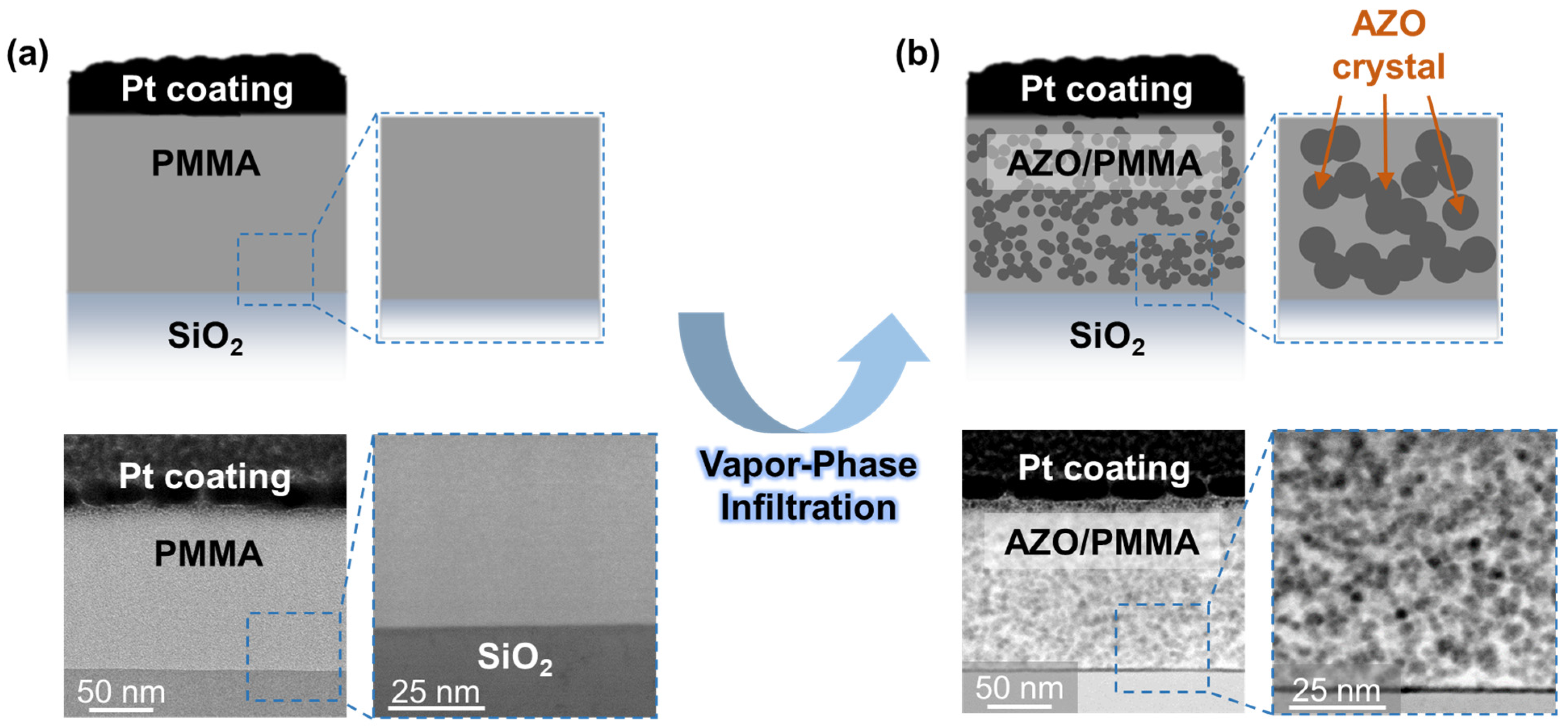
Figure 1 illustrates the formation process of AZO within a poly(methyl methacrylate) (PMMA) film, resulting in an AZO/PMMA hybrid film [
25]. The amorphous structure of the spin-coated PMMA film is clearly shown in
Figure 1a by transmission electron microscopy (TEM) images. In the amorphous PMMA polymer, “free volume” refers to the angstrom-to-nanometer-scale intermolecular void space between polymer chains that is inherently present throughout the polymer interior, providing molecular-scale pathways that enable the diffusion of small gaseous molecules [
25,
30]. Vapor-phase infiltration (VPI) of Al-doped zinc oxide (AZO) was facilitated by exposing the PMMA film to high-pressure vapor of AZO precursors (diethylzinc (DEZ), trimethylaluminum (TMA), and water). The VPI process begins by evacuating the chamber to a base pressure. Pure precursor vapor is then introduced into the chamber without a carrier gas, with the outlet valve closed. The precursor vapor is thereby kept inside the chamber at a desired exposure pressure for controlled durations to perform chemical reactions with the polymer matrix. During the exposure step, the small gaseous precursor molecules can penetrate the polymer chains in the subsurface region through the free volume. The gas molecules primarily reside within free volume cavities, with intermittent transitions to neighboring sites through temporary pathways, following the concept established in our previous work [
25]. The degree of gas penetration varies with VPI conditions such as precursor vapor pressure, exposure time, and temperature. Finally, the inert gas flows through the chamber to remove the residual precursor molecules and by-products of the chemical reactions. These four steps are then repeated for the other precursor to complete one VPI cycle (
Figure S1).
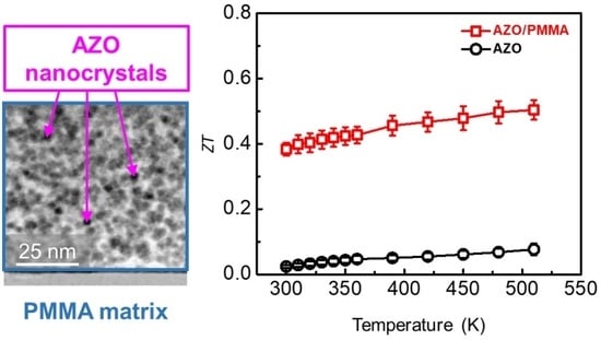
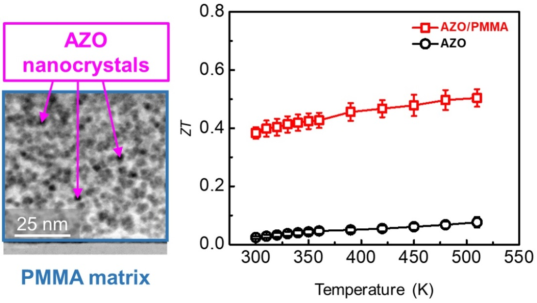
Figure 1b shows a high-resolution TEM image of the AZO/PMMA hybrid layer at a thickness of 150 nm, revealing a more heterogeneous structure compared to pure PMMA. This magnified view highlights the nanoscale interactions between AZO and PMMA, showing the presence of AZO nanocrystals within the PMMA matrix and suggesting that the AZO precursors penetrate the free volume within the polymer chains. The AZO nanoparticles observed in the TEM image have a relatively uniform distribution with particle sizes of approximately 3–5 nm. This can be attributed to the uniform distribution of the C=O functional groups inside the PMMA chains, which can react with DEZ/TMA molecules in the free volume of the PMMA film, as identified in previous studies [
21,
23,
31]. Similarly, the oxygen precursor, water, can diffuse into the PMMA film and react with the chemisorbed metal-organic species to form ZnO or Al
2O
3. After multiple VPI cycles, the AZO within the PMMA nearly fills the free volume. The size of AZO nanocrystals tends to increase with the number of VPI cycles. Therefore, the number of VPI cycles is an important parameter for ensuring the effective infiltration of AZO into PMMA.
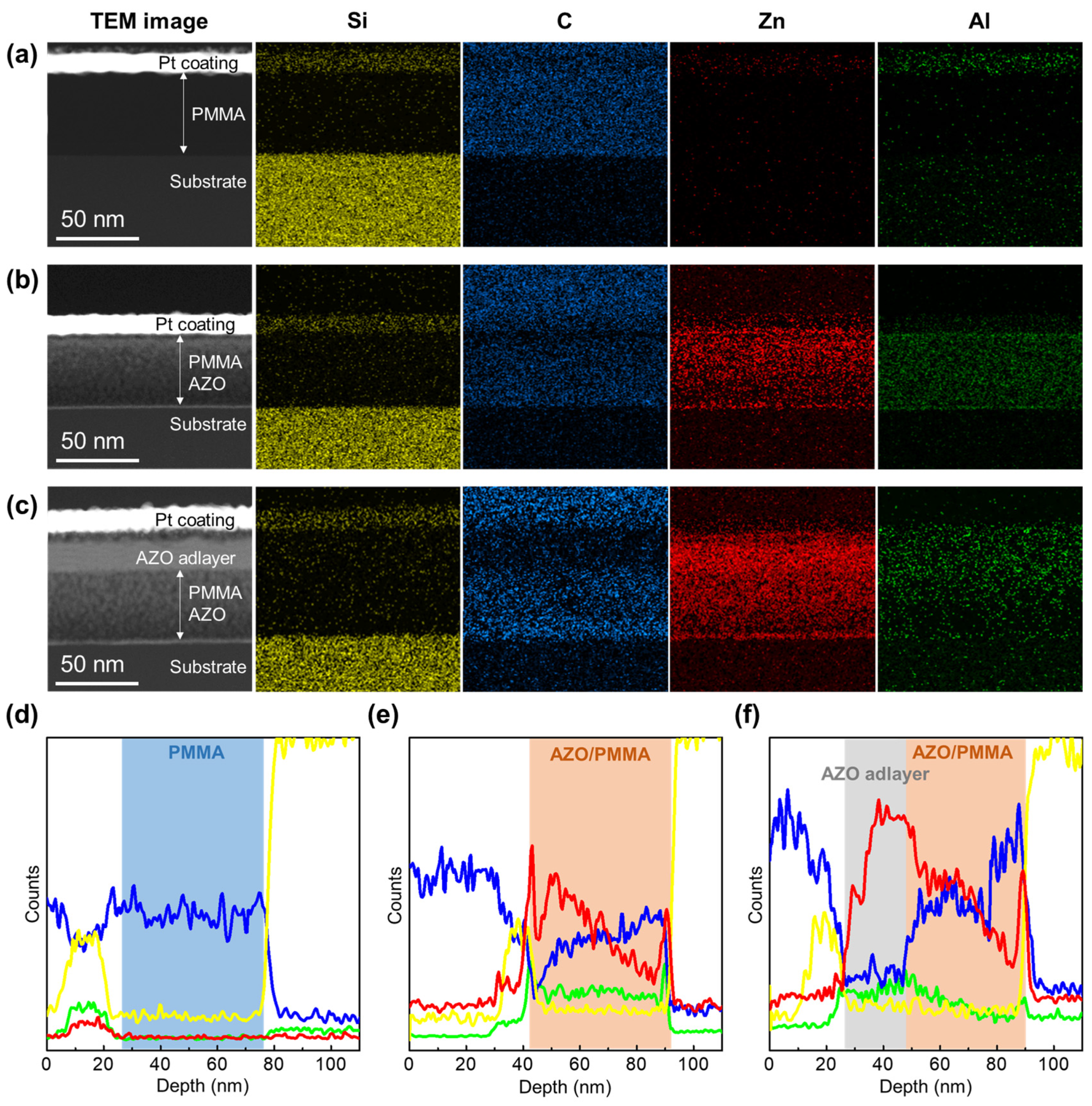
To examine the combined effect of VPI parameters on the penetration depth of AZO within the PMMA films, cross-sectional transmission electron microscopy (TEM) and energy-dispersive X-ray spectroscopy (EDS) were employed (
Figure 2).
Figure 2a displays a pristine PMMA film coated with a thin platinum (Pt) layer for TEM imaging purposes. The PMMA film exhibits a uniform and amorphous structure, with a 50 nm thick layer and a clear boundary with the underlying silicon oxide (SiO
2) substrate. The corresponding TEM image (
Figure 2b) shows the formation of an AZO/PMMA hybrid layer following infiltration. As shown in
Figure 2b, the hybrid layer maintains a thickness of 50 ± 2 nm. In contrast, a similar analysis of a PMMA film with an overlying AZO layer reveals a thicker AZO adlayer on top (
Figure 2c). The thicknesses of the layers were measured from TEM images acquired at ten different locations on each type of film. EDS was performed at the same locations where TEM images were acquired to map the elemental composition. The EDS maps show that the hybrid layer contains aluminum, oxygen, and zinc signals attributable to AZO, as well as a carbon signal from PMMA (
Figure 2b). The presence of C, Al, and Zn signals in the EDS data confirmed that AZO infiltrated into the PMMA film during the VPI process, forming an organic–inorganic hybrid layer through AZO nucleation within the free volume of PMMA. In contrast, the AZO adlayer deposited on top of the PMMA film exhibits Al and Zn signals without a detectable C signal, indicating the formation of pure AZO.
Figure 2d–f show the out-of-plane elemental composition profiles of Si, C, Al, and Zn extracted from EDS mappings of bare PMMA and AZO/PMMA films. The Si signal clearly identifies the SiO
2 substrate region in all profiles. In bare PMMA (
Figure 2d), the C signal remains nearly constant throughout the 50 nm thick film, consistent with the uniform amorphous structure of PMMA. In contrast, distinct Al and Zn signals are observed throughout the AZO/PMMA film (
Figure 2e), confirming successful AZO infiltration. The Zn signal gradually decreases from the film surface toward the substrate, accompanied by a corresponding increase in the C signal. This depth-dependent distribution is attributed to preferential AZO nucleation and growth near the polymer surface, where precursor accessibility and reactivity are higher [
32].
Based on this mechanism, a 50 nm thick PMMA film was selected to ensure AZO distribution throughout the entire film thickness. Comparison of the two VPI conditions demonstrates that careful control of the VPI cycle number enables AZO infiltration without adlayer formation, as evidenced by the absence of an adlayer in
Figure 2b compared with its clear presence in
Figure 2c.
Figure 2f further confirms adlayer formation under excess VPI cycles, showing strong AZO signals and negligible C intensity near the film surface. AFM measurements further reveal low root-mean-square (RMS) roughness of ~0.30 nm and ~0.40 nm for bare PMMA and AZO/PMMA hybrid film, respectively (
Figure S2), confirming high film uniformity over a 5 µm × 5 µm scan area and indicating that the VPI process does not significantly alter the surface morphology.
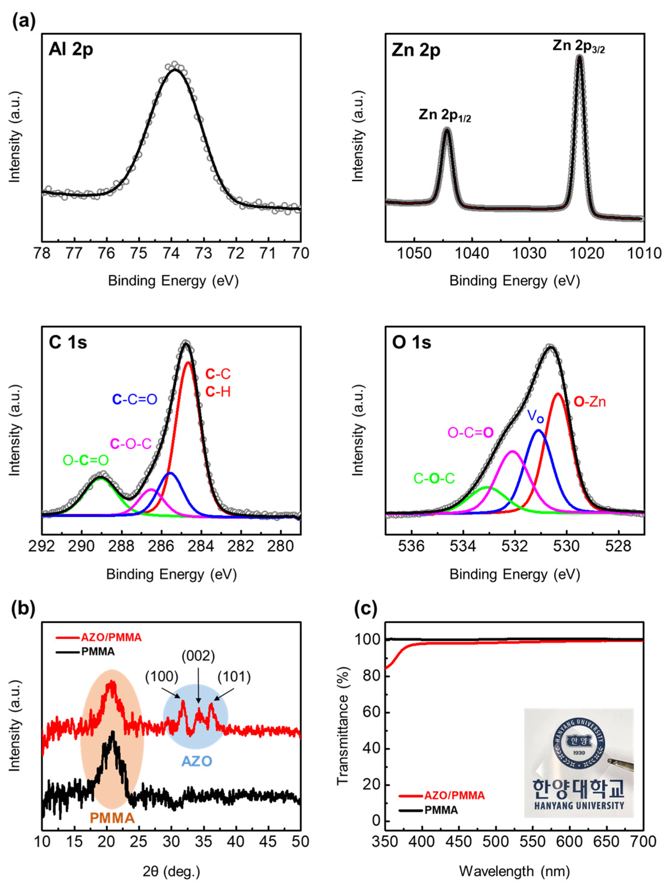
The chemical composition of AZO/PMMA was confirmed by high-resolution X-ray photoelectron spectroscopy (XPS) in
Figure 3a. The Zn 2p
3/2 and Zn 2p
1/2 peaks were centered at binding energies of 1021.2 and 1044.3 eV, respectively, and the Al 2p peak was located at approximately 73.8 eV, consistent with the characteristic XPS peaks of AZO reported in the literature [
28,
33]. In contrast, the Al 2p and Zn 2p regions of the bare PMMA film show no detectable signals (
Figure S2), confirming the absence of AZO in the uninfiltrated film. The C 1s XPS peaks exhibit four main components located at approximately 289.1, 286.5, 285.5, and 284.6 eV, corresponding to O-C=O, C-O-C, C-C=O, and C-C/C-H bonding, respectively, which are characteristic of PMMA. Notably, the O 1s spectrum of the AZO/PMMA film can be deconvoluted into four components at the binding energies of 533.1, 532.0, 531.2, and 530.3 eV, corresponding to the C-O-C and O-C=O groups in PMMA, as well as oxygen vacancies (V
O) and O-Zn in AZO. These results are consistent with previous studies [
24,
34], demonstrating the chemical composition of the hybrid AZO/PMMA film. In contrast, the O 1s XPS spectrum of bare PMMA shows only O-C=
O and C-
O-C bonding assigned to the PMMA chains, while the C 1s spectrum exhibits peaks similar to those of the AZO/PMMA film.
Figure 3b presents the X-ray diffraction (XRD) patterns of the pure PMMA and AZO/PMMA films. The XRD pattern of pure PMMA shows a broad peak indicative of its amorphous nature [
11]. However, the XRD pattern of the AZO/PMMA hybrid film reveals both the broad amorphous background and additional peaks corresponding to AZO nanocrystals at 31.75°, 34.25°, and 36.15°. These peak positions are consistent with (100), (002), and (101) diffraction planes of AZO nanocrystals [
33], confirming the successful infiltration of AZO nanocrystals into the PMMA matrix. The hybrid thin film also demonstrated high optical transparency in the visible range, as depicted in
Figure 3c. The transmittance spectrum of the 100 nm-thick AZO/PMMA hybrid film on a quartz substrate exhibited light transmittance greater than 95% across the visible range (400–800 nm). This high transparency underscores its broad applicability for energy-harvesting components in transparent electronics and smart windows.
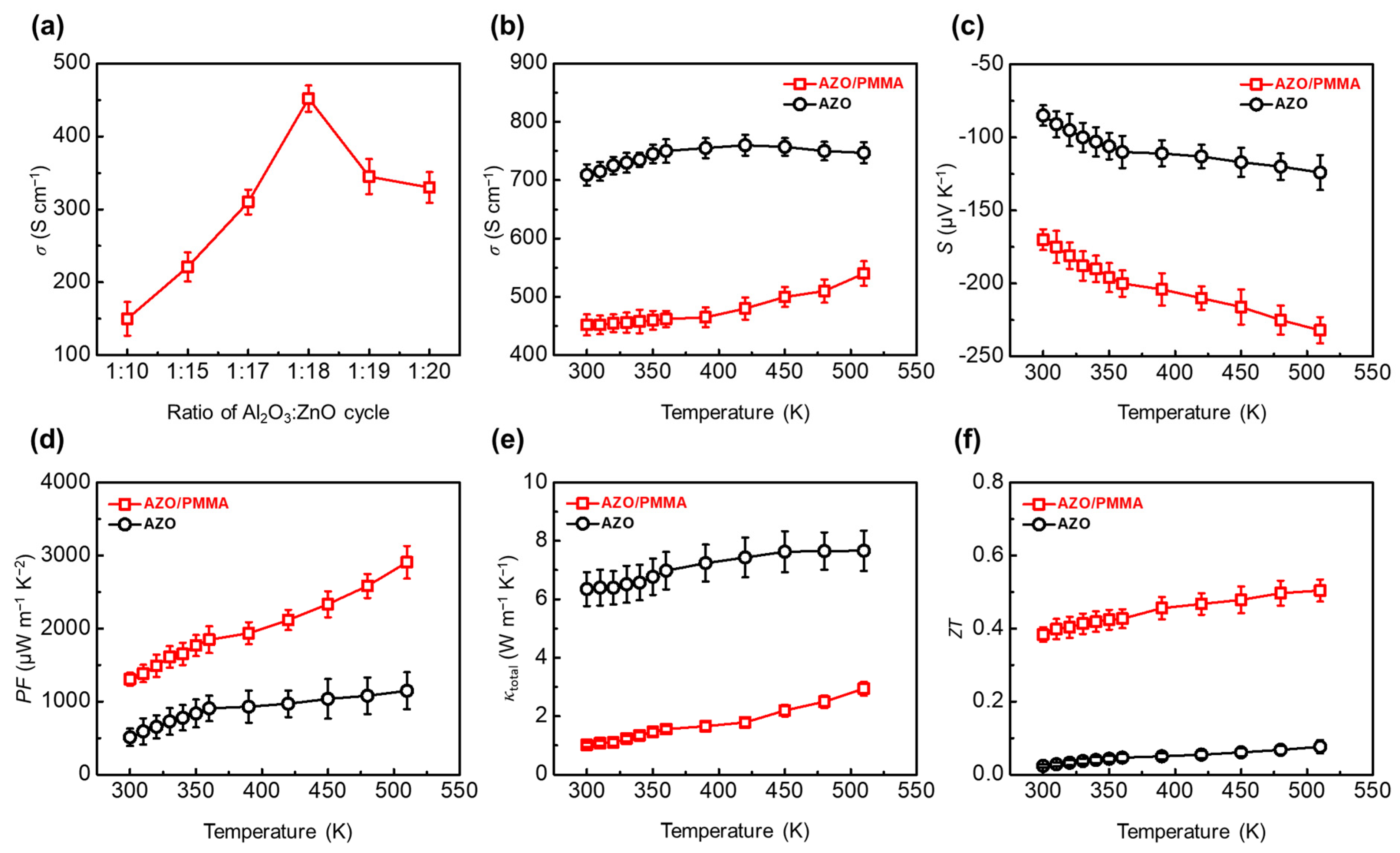
Figure 4 illustrates the thermoelectric properties of the AZO/PMMA hybrid film compared to those of the AZO film without PMMA. To optimize the electrical conductivity (
σ) of the AZO/PMMA films, various Al
2O
3-to-ZnO ratios were investigated (
Figure 4a). The Al
2O
3-to-ZnO ratio was controlled by adjusting the VPI sequence, specifically by varying the number of ZnO cycles per single Al
2O
3 cycle. AZO/PMMA films fabricated under each condition were then characterized for electrical conductivity. The results indicate that the peak electrical conductivity, 452 S cm
−1, was achieved with an Al
2O
3-to-ZnO cycle ratio of 1:18, suggesting an optimal doping level at which aluminum effectively increases electron concentration without introducing excessive lattice defects. However, as the doping ratio increased beyond this point, the electrical conductivity began to decrease. This decrease can be attributed to the increased scattering of charge carriers due to the excessive generation of defects and dislocations within the ZnO lattice, as well as the saturation of donor levels, which limits the contribution of additional Al dopants to carrier concentration and reduces overall carrier mobility. These results are consistent with findings from other studies on the effects of Al-doping concentrations on the electrical properties of AZO [
33]. After infiltrating AZO into PMMA, the Seebeck coefficient (
S) at room temperature increased from −85.0 μV K
−1 for the AZO film to −170 μV K
−1 for the AZO/PMMA hybrid film, while the electrical conductivity decreased from 709 S cm
−1 to 452 S cm
−1. These results indicate that electron transport is strongly influenced by carrier scattering at the AZO/PMMA interfaces. In conventional composite systems, incorporation of an insulating secondary phase such as PMMA primarily disrupts the conductive pathways, resulting in reduced electrical conductivity, while the Seebeck coefficient is expected to remain close to that of the conducting phase (AZO) according to the dilution model [
35], since PMMA contributes negligibly to carrier transport. However, following AZO infiltration into PMMA, the magnitude of the Seebeck coefficient nearly doubles, far exceeding the value predicted by the dilution model. This pronounced enhancement supports the presence of an energy filtering mechanism at the AZO/PMMA interfaces. Energy filtering is a process in which low-energy electrons are selectively scattered at the interfaces, preventing them from contributing to electrical conduction, while high-energy electrons pass through. This selectivity increases the average energy of the conducting electrons and, in turn, enhances the Seebeck coefficient [
18,
27]. Although the electrical conductivity decreases, the improvement in the Seebeck coefficient is more pronounced, ultimately increasing the power factor. The energy filtering effect is particularly evident in composite materials with heterogeneous interfaces, such as AZO/PMMA hybrid films, and plays a crucial role in enhancing thermoelectric performance in nanocomposites [
14]. Consequently, the power factor of the AZO/PMMA hybrid film at room temperature reaches 1306 μW m
−1 K
−2, which is significantly higher than the 512 μW m
−1 K
−2 of the AZO film. As the temperature rises, these barriers preferentially scatter low-energy carriers while allowing high-energy carriers to pass through. This selective scattering increases the average energy of the conducting carriers, thereby enhancing
S. Simultaneously, thermal activation enables more carriers to overcome these barriers, leading to an increase in
σ.
The thermal conductivities of the pure AZO film and the AZO/PMMA hybrid film were measured to be 6.35 W m
−1 K
−1 and 1.02 W m
−1 K
−1, respectively, at room temperature. To further analyze the mechanism behind this significant reduction in thermal conductivity, we investigated the contributions of electronic thermal conductivity (
κE) and lattice thermal conductivity (
κL) separately. The electronic thermal conductivity (
κE) was calculated using the Wiedemann–Franz relation
κE =
σLT, where
σ is the electrical conductivity,
T is the absolute temperature, and
L is the Lorenz number. The Lorenz number
L was estimated from the Seebeck coefficient (
S) following the equation
L = 1.5 + exp(−∣
S∣/116) [
5]. The AZO film exhibited an electronic thermal conductivity of approximately 0.421 W m
−1 K
−1, while the AZO/PMMA hybrid film showed a value of 0.235 W m
−1 K
−1. Although the electrical conductivities of the two samples differ, the corresponding changes in the Lorenz number result in comparable
LT products. Consequently, the electronic thermal conductivities of the two samples remain within the same order of magnitude despite their differing electrical conductivities. This indicates that the dominant contribution to the total thermal conductivity (
κtotal) reduction arises from the decrease in lattice thermal conductivity. The lattice thermal conductivity (
κL) for both samples was calculated using
κL =
κtotal −
κE. The lattice thermal conductivity of the AZO/PMMA hybrid film was found to be significantly lower than that of the AZO film. Specifically, at room temperature, the
κL of the AZO film was approximately 5.93 W m
−1 K
−1, whereas that of the AZO/PMMA hybrid film was approximately 0.785 W m
−1 K
−1. This substantial reduction in lattice thermal conductivity can be attributed to phonon scattering at the AZO/PMMA interfaces [
3]. In nanocrystalline AZO films, the phonon mean free path is significantly reduced by grain-boundary scattering, rendering
κL relatively insensitive to additional phonon–phonon scattering at elevated temperatures. In contrast, according to the Wiedemann–Franz law, the electronic contribution
κE increases with temperature owing to both the linear dependence of
κE on
T and thermally assisted carrier transport across grain boundaries. As a result, the electronic contribution increasingly dominates thermal transport at elevated temperatures. In the AZO/PMMA hybrid films, the increase in
κ with temperature arises from two concurrent contributions. The amorphous PMMA matrix itself exhibits an intrinsically increasing
κ with temperature, consistent with previous experimental observations [
36]. In addition, the infiltrated AZO network contributes to thermal transport in a manner similar to that observed for the pristine AZO film. Consequently, the combined contributions of the polymer matrix and embedded AZO network lead to the monotonic increase in
κ observed for the AZO/PMMA hybrid films.
The substantial increase in the Seebeck coefficient and the significant reduction in thermal conductivity resulted in a
ZT value of 0.384 at room temperature for the AZO/PMMA hybrid film. The room-temperature transport parameters of the AZO/PMMA hybrid film and various composites are summarized in
Table S1, which lists the electrical conductivity (
σ), Seebeck coefficient (
S), power factor (
PF), thermal conductivity (
κ), temperature (
T), and thermoelectric figure of merit (
ZT) for each material. The room-temperature figure of merit of AZO/PMMA shows significantly improved results compared to other reported metal oxide–polymer composites [
15,
17,
19,
37,
38,
39,
40]. This result demonstrates that VPI can disperse AZO more uniformly within the PMMA film, enhancing interface scattering and thus improving thermoelectric properties. In conclusion, by infiltrating AZO into the PMMA matrix, we achieved simultaneous enhancement of the Seebeck coefficient and suppression of thermal conductivity, while maintaining adequate electrical conductivity, resulting in enhanced thermoelectric performance.
3. Materials and Methods
3.1. Preparation of Substrates
For structural and thermoelectric property evaluation, samples were prepared on 300 nm SiO2 substrates thermally grown on p-type Si wafers (Seyang Electronics). The SiO2/Si substrates were cut to the necessary dimensions and underwent a thorough cleaning process. This included an alkaline treatment in boiling NH4OH solution, followed by an acid treatment in boiling HCl solution, with multiple deionized water (DI water) rinses in between. Finally, the substrates were dried using nitrogen gas to completely remove any remaining surface contaminants.
3.2. Fabrication of Al Doped ZnO Thin Films and AZO/PMMA Thin Films
The deposition of Al-doped ZnO thin films for reference was conducted in a custom-built atomic layer deposition (ALD) chamber at a pressure of 1.0 Torr. For ALD, argon (Ar, 99.99% purity) was used as both the carrier and purging gas at a constant flow rate of 200 sccm. Thin films were deposited onto the cleaned SiO2/Si substrates at 100 °C. Each ZnO ALD cycle consisted of a 20 s exposure to diethyl zinc (DEZ, Sigma-Aldrich, St. Louis, MO, USA, Zn 52 wt%), followed by a 60 s Ar purge, a 20 s H2O exposure, and a 100 s Ar purge to form a ZnO layer. To achieve Al doping, Al2O3 was deposited on the ZnO nanolayers. The doping layer ALD process included a 3 s exposure to trimethylaluminum (TMA, Sigma-Aldrich, St. Louis, MO, USA, 97%), followed by a 40 s Ar purge, a 3 s H2O exposure, and a 60 s Ar purge, all at 100 °C.
To fabricate AZO-infiltrated PMMA samples, poly(methyl methacrylate) (PMMA, Sigma-Aldrich, St. Louis, MO, USA, MW: 350,000 g/mol) was dissolved in chlorobenzene (Sigma-Aldrich, St. Louis, MO, USA, 99%) at a weight ratio of 1:5, yielding a 16.7 wt% solution. The solution was spin-coated onto the cleaned substrates using a Spin-1200D spin coater (Midas, Daejeon, Republic of Korea) at 4000 rpm for 75 s, resulting in a nominal thickness of 50 nm. Subsequently, AZO infiltration was performed on the spin-coated PMMA. The vapor-phase infiltration (VPI) sequences involve evacuation, precursor dosing, exposure, and purging steps. During the exposure step, the substrates were subjected to a high-pressure precursor in a closed chamber. This high-pressure exposure step distinguishes VPI from conventional ALD, in which precursors are continuously dosed with a carrier gas under dynamic flow conditions. The Al2O3 infiltration cycle involved 20 s of evacuation and dosing TMA at 1 Torr, followed by exposing the substrates for 100 s with the chamber lines and gate closed. After this, the chamber was purged for 200 s. Subsequently, the chamber was evacuated for 20 s prior to H2O dosing at 1 Torr, followed by a 100 s exposure and a 300 s purge. Similarly, the ZnO cycle began with a 20 s evacuation, followed by dosing DEZ at 1 Torr, a 100 s exposure, and a 200 s purge. After another 20 s of evacuation, H2O was dosed at 1 Torr, followed by a 100 s exposure and a 300 s purge. The temperature during the deposition process was maintained at 100 °C. To achieve the optimized AZO composition, one Al2O3 infiltration cycle was followed by 18 ZnO infiltration cycles. According to the EDS data, the ratio of Al to Zn was determined to be 1.09:8.26.
3.3. Characterization of Surface Morphology and Crystallinity Properties
The thickness and surface morphology of the samples were analyzed using a spectroscopic ellipsometer (FS-1, Film Sense, Lincoln, NE, USA) and an atomic force microscope (AFM, XE-100, Park Systems, Suwon, Republic of Korea), respectively. The microstructure of the PMMA and AZO/PMMA hybrid films was examined by a transmission electron microscope (TEM, JEM-ARM200F, JEOL, Tokyo, Japan) at 200 kV. For cross-sectional TEM analysis, specimens were prepared via a focused ion beam (FIB, Helios G5 UC, Thermo Fisher, Waltham, MA, USA). Samples were coated with carbon and platinum before FIB processing to protect the surface from ion beam damage. The cross-sectional line scan profiles were built via ImageJ software (version 1.54s) from EDS mappings. The crystallinity of ZnO was assessed via grazing incidence X-ray diffraction (GI-XRD) using a multipurpose high-resolution X-ray diffractometer (HR-XRD, Smartlab, Rigaku, Osaka, Japan). The X-ray photoelectron spectroscopy (XPS) data were acquired by a PHI-GENESIS (Ulvac-PHI, Chigasaki, Japan) spectrometer equipped with a monochromatic micro-focused Al Kα X-ray source. Transmittance spectra of the thin films were recorded with a UV-Vis spectrometer (Cary 5000, Agilent, Santa Clara, CA, USA).
3.4. Thermoelectric Characterization
The electrical conductivity (
σ) and Seebeck coefficient (
S) of the samples along the in-plane direction were measured simultaneously utilizing a thermoelectric analyzer (Linseis-LSR 3, Linseis, Robbinsville, NJ, USA) on films deposited on SiO
2 substrates (1 cm × 2.5 cm). To measure the in-plane thermal conductivity (
κ), we used a commercially available Linseis thin film analyzer (TFA) chip [
39] using van der Pauw geometry. Initially, the chip was patterned via a polystyrene resin mask from Linseis. To avoid undesired backside deposition on the TFA chip’s suspended membrane, we covered the sample edges with polyimide tape, which ensured the accuracy and reliability of the measurement. Thermal conductivity was estimated using a 3-ω measurement technique with a thin film analyzer (Linseis-TFA Linseis, Robbinsville, NJ, USA). All measurements were conducted on at least 10 independently fabricated sample batches, with each sample measured three times. The standard deviations for
σ,
S, and
κ were within ±4.5%, ±10%, and ±9.5%, respectively.



 ,
,