1. Introduction
In high-energy-consumption industries like Aiye processing equipment, steel, chemical, and cement, vast amounts of medium- to low-temperature waste heat are directly discharged [
1,
2]. Oxide thermoelectric modules can capture this waste heat and convert it into useful electricity, enabling cascading energy use and improving overall energy efficiency [
3,
4,
5]. Thermoelectric generators can convert this into electricity to power onboard systems, reducing engine load and thereby lowering fuel consumption and emissions [
6,
7,
8]. In remote areas, space probes, or IoT sensor nodes where battery replacement is difficult, thermoelectric materials can enable long-term, stable power generation using radioisotopes or natural temperature differences (e.g., geothermal, body heat). Compared to traditional alloy thermoelectric materials, oxide thermoelectrics offer several distinct advantages. Being oxides, these materials are inherently stable in air and can operate long-term at high temperatures (typically above 500 °C) without complex vacuum or inert gas protection. This greatly simplifies system architecture, enhances reliability, and reduces maintenance costs. Their main constituent elements (e.g., Cobalt, Manganese, Strontium, Calcium) are abundant in the earth’s crust and relatively inexpensive, far cheaper than the rare/expensive elements (like Tellurium, Bismuth) required in materials such as Bismuth Telluride [
9,
10]. They contain no toxic or heavy metal elements, making them more environmentally friendly during production and use, aligning with green and sustainable development goals. Their preparation methods (e.g., solid-state reaction, sintering) are compatible with traditional ceramic processes, facilitating large-scale production and helping to reduce manufacturing costs. Although their thermoelectric figure of merit (ZT) is generally lower than that of some top-performing alloy materials, oxide thermoelectric materials, by virtue of their exceptional high-temperature stability, cost advantages in raw materials, and environmental friendliness, are demonstrating strong viability and broad commercialization prospects in the highly potential application field of medium- to high-temperature waste heat power generation [
11,
12].
Indium oxide, a typical transparent oxide semiconductor, has also garnered significant attention in the field of thermoelectric materials. Its crystal structure is typically a cubic bixbyite structure. However, despite years of research, the intrinsic thermoelectric performance of bulk indium oxide, particularly its figure of merit (ZT), remains relatively low, limiting its practical application [
13,
14]. The current research landscape primarily focuses on understanding and addressing these core bottlenecks. The main bottleneck for the thermoelectric performance of indium oxide lies in the difficulty of achieving a high power factor. The power factor, a key parameter measuring a material’s ability to output electrical power per unit temperature difference and gradient, is determined by the product of the square of the Seebeck coefficient and the electrical conductivity. Indium oxide faces a classic trade-off in this regard. Undoped, pure indium oxide has a very low intrinsic carrier concentration due to its relatively wide band gap, resulting in very poor electrical conductivity, behaving like an insulator or semiconductor. While introducing dopants (such as Tin, Zinc, Cerium) can effectively increase carrier concentration and significantly enhance conductivity, this inevitably leads to the next problem [
15,
16,
17]. A critical challenge for In
2O
3 thermoelectrics is the inherent trade-off between electrical conductivity (enhanced by heavy doping) and Seebeck coefficient (inversely related to carrier concentration), stagnating its power factor. Its lattice thermal conductivity remains insufficiently low due to weak phonon scattering, further suppressing ZT. Despite environmental friendliness and stability, decoupling electron-phonon transport via band engineering and microstructure control is key for future breakthroughs.
Among numerous dopants for optimizing In2O3 thermoelectric properties, Yb introduction boasts unprecedented innovations and unique advantages that transcend traditional doping paradigms. Its core innovation lies not in mere charge carrier regulation, but in an innovative “phonon scattering-electron transport” decoupling mechanism—an original approach that synergistically optimizes thermoelectric performance, stemming from Yb’s unique multi-role behavior in the In2O3 lattice, a breakthrough distinct from single-function dopants. The significant ionic radius difference between Yb3+ and In3+ induces severe lattice distortion and strain field fluctuations, forming strong point defects that efficiently scatter mid-to-high-frequency phonons, a more effective phonon scattering pathway than dopants with better ionic radius matching. This innovative scattering effect drastically reduces lattice thermal conductivity, a key ZT-enhancing step. More innovatively, Yb doping subtly modifies the band structure via advanced “band engineering”—introducing impurity bands or band convergence to increase density of states effective mass—resolving In2O3’s core low power factor issue by maintaining high carrier concentration while boosting the Seebeck coefficient. Additionally, Yb3+’s stable electronic shell structure preserves In2O3’s high-temperature stability, resolving the long-standing performance-stability conflict critical for commercialization. Most innovatively, Yb transcends traditional dopants’ single carrier-regulation role, using three synergistic mechanisms to simultaneously optimize ZT’s numerator (power factor) and denominator (thermal conductivity), offering a pioneering solution to In2O3’s inherent trade-offs.
2. Results and Discussion
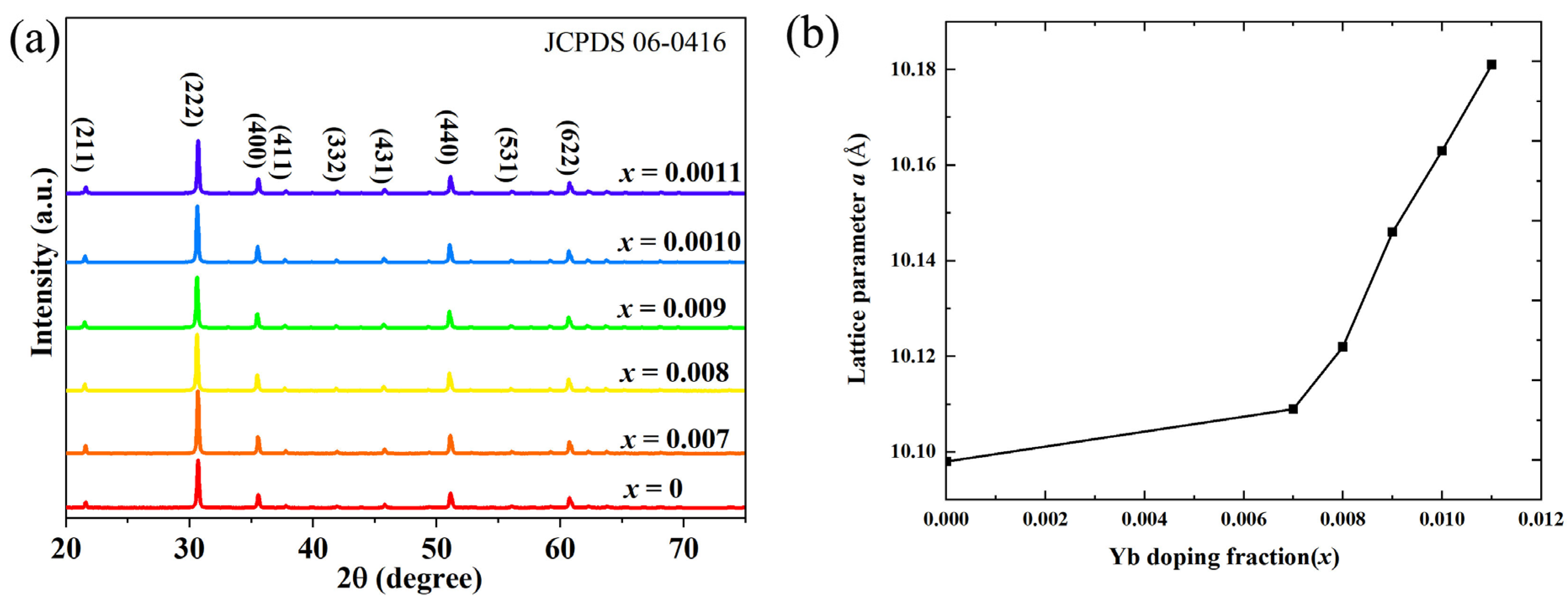
Figure 1 presents the X-ray diffraction (XRD) patterns and lattice constant results of Yb
2O
3-doped indium oxide thermoelectric materials. From the XRD patterns, it is evident that all diffraction peaks perfectly match the standard card of cubic indium oxide (In
2O
3, space group Ia-3), with no additional peaks observed. This indicates that, under the current experimental conditions, even with the introduction of Yb
2O
3 dopant, no detectable secondary phases or impurity phases have formed. In other words, Yb
3+ ions have successfully entered the In
2O
3 lattice, forming a homogeneous solid solution without precipitating independent secondary phases such as Yb
2O
3 or other complex oxides. The results show that the lattice constants of the doped samples are significantly larger than those of pure In
2O
3, and the lattice constant increases monotonically with higher doping levels. The fundamental reason for this lattice expansion lies in the difference in ionic radii between Yb
3+ and In
3+. The ionic radius of In
3+ is approximately 80 pm, while that of Yb
3+ is about 98.5 pm. Since the ionic radius of Yb
3+ is significantly larger than that of In
3+, when Yb
3+ substitutes for In
3+ sites in the In
2O
3 lattice, it introduces local lattice distortion. To accommodate the larger cation, the surrounding oxygen ion framework is forced to expand outward, resulting in an increased unit cell volume, which macroscopically manifests as an increase in the lattice constant. This lattice expansion caused by the substitution of a larger ion for a smaller one is a common “size effect” in solid solution systems.
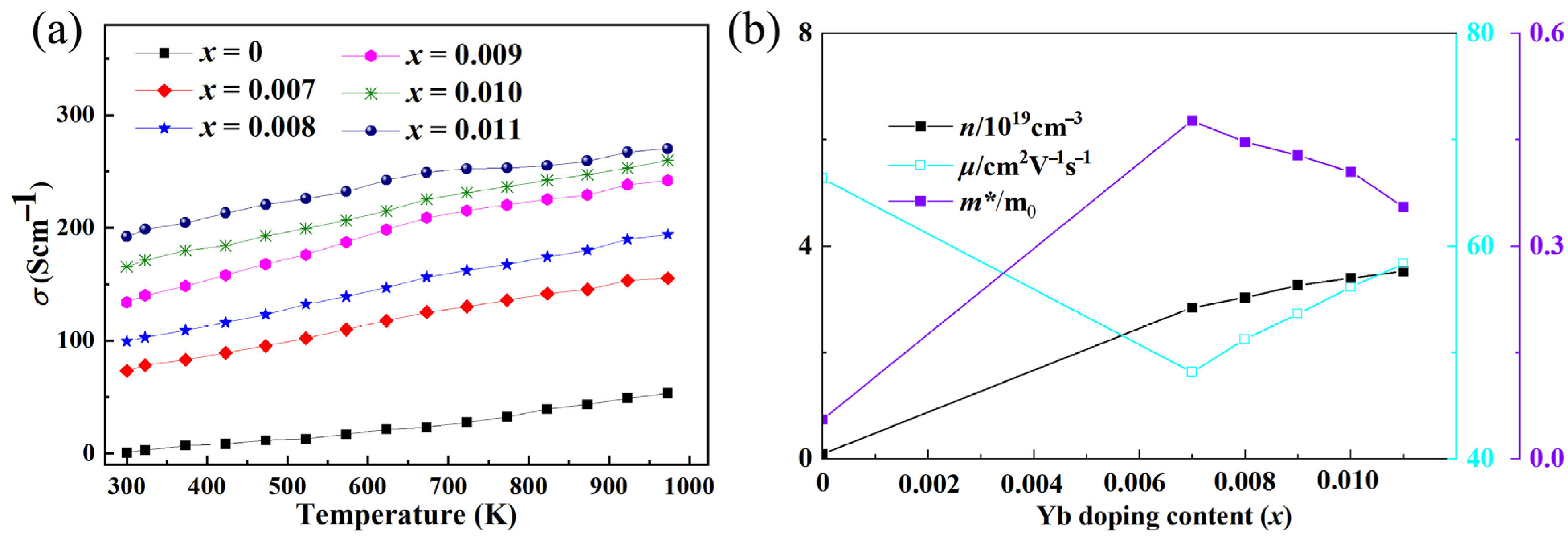
In the Yb
2O
3-doped In
2O
3 system, the electrical conductivity showed a significant increasing trend, as shown in
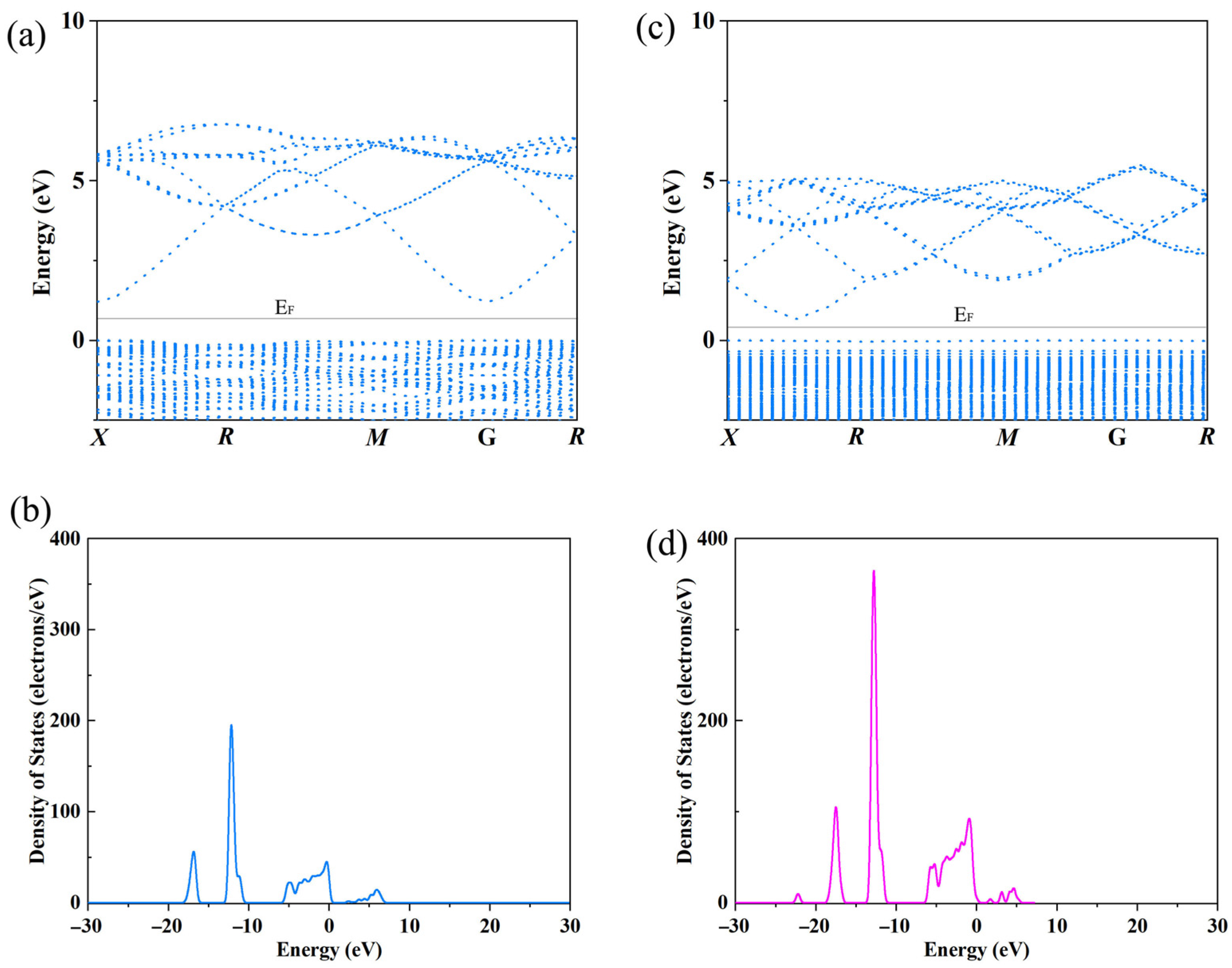
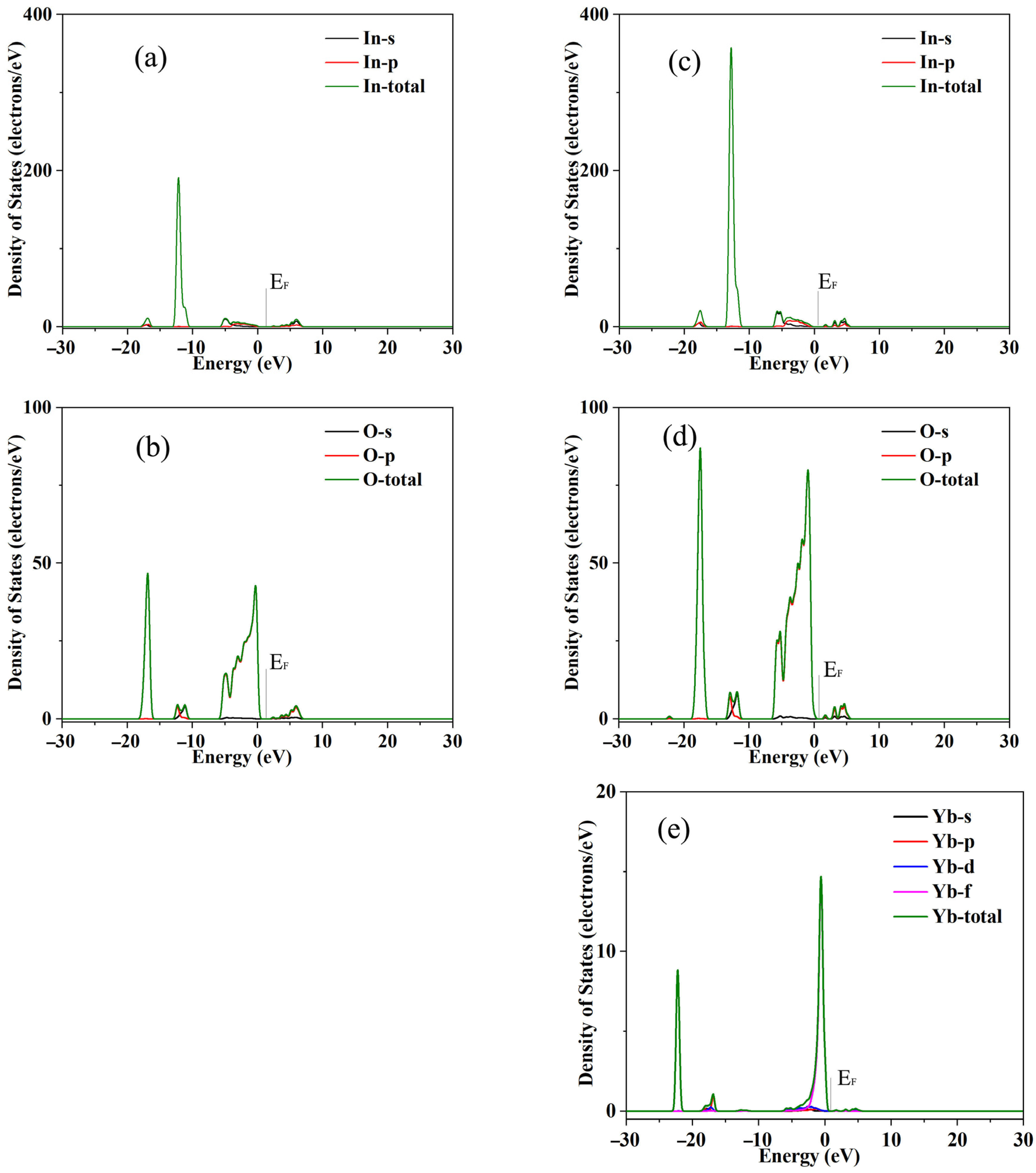
Figure 2, accompanied by the enhancement of carrier concentration, the decrease in carrier mobility, the narrowing of band gap, and the increase in density of states (DOS) near the Fermi level as shown in
Figure 3 and
Figure 4. As a core electrical transport parameter of thermoelectric materials, the variation law of electrical conductivity directly determines the thermoelectric conversion efficiency of materials, and its evolution mechanism is closely related to the electronic structure reconstruction, defect formation, and microstructural changes induced by doping. In
2O
3 adopts a body-centered cubic bixbyite structure with space group Ia-3, in which In
3+ occupies two non-equivalent cation sites and O
2− ions form a distorted close-packed array. Undoped In
2O
3 exhibits intrinsic n-type conductivity due to native oxygen vacancies that act as shallow donors and provide electrons to the conduction band. When Yb
2O
3 is doped into the In
2O
3 lattice, although Yb
3+ substitutes In
3+ isovalently, massive point defects are generated under the driving force of lattice chemical potential equilibrium and defect formation thermodynamics. According to the conductivity formula σ = nqμ, electrical conductivity is determined by both carrier concentration (n) and mobility (μ). With increasing Yb
2O
3 doping content, carrier concentration increases continuously due to the formation of high-density oxygen vacancies with lower formation energy than intrinsic vacancies. Notably, carrier mobility first decreases and then increases with rising doping level. At low doping, lattice distortion and defect scattering induced by ionic radius mismatch dominate, leading to reduced mobility. As doping further increases, improved electronic structure, delocalized band states and optimized defect distribution weaken scattering effects, resulting in a recovery of mobility. The substantial increase in carrier concentration remains dominant, leading to an overall enhancement in electrical conductivity. Yb doping also reshapes the electronic structure of In
2O
3. Orbital interactions between dopant and host ions narrow the band gap, introduce impurity levels, and increase the density of states near the Fermi level, which facilitates carrier excitation and transport. Band gap narrowing reduces the effective electron mass, which further moderates mobility degradation. Excessively high doping may still cause defect aggregation and strong scattering, limiting further conductivity improvement. The trade-off and synergistic evolution between carrier concentration and mobility reveal the complex electronic transport mechanism in Yb-doped In
2O
3. Rational doping regulation can achieve balanced carrier transport and optimized thermoelectric properties.
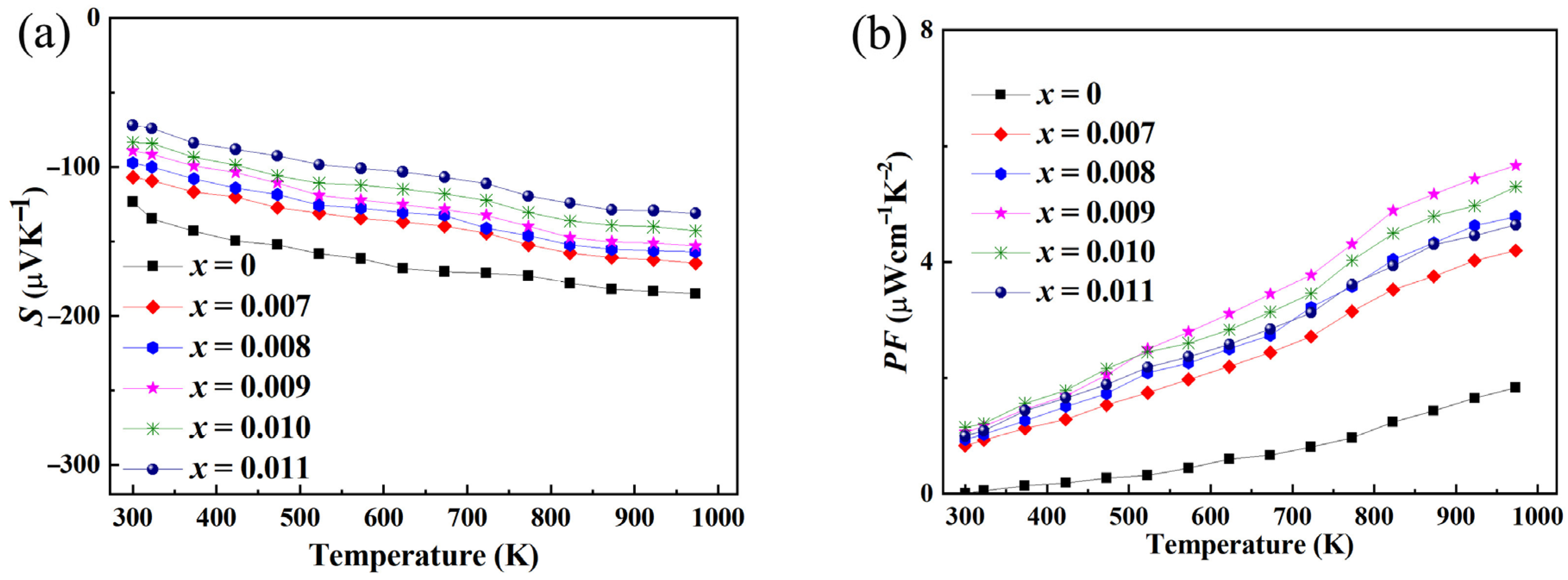
Figure 5 presents the measured Seebeck coefficient of Ytterbium Oxide (Yb
2O
3)-doped Indium Oxide (In
2O
3) thermoelectric material. The reduced absolute Seebeck coefficient after Yb
2O
3 doping mainly results from increased carrier concentration. Yb
3+ substituting In
3+ promotes oxygen vacancies, which donate free electrons to elevate conduction band electron concentration. According to the fundamental theory of the Seebeck coefficient, for degenerate or heavily doped semiconductors, the Seebeck coefficient (S) and carrier concentration (n) approximately follow the relation: |S| ∝ 1/n^(2/3) [
18]. This relation clearly indicates that the absolute value of the Seebeck coefficient is inversely proportional to the 2/3 power of the carrier concentration. Therefore, when Yb
2O
3 doping causes a sharp increase in carrier concentration n, the absolute value |S| inevitably decreases significantly. The increase in electrical conductivity (σ) and the decrease in the Seebeck coefficient are closely interrelated manifestations of the same physical process (increased carrier concentration). As mentioned, Yb
2O
3 doping causes a substantial increase in n. Even if the mobility μ decreases due to enhanced scattering, the dramatic increase in n usually dominates overwhelmingly, leading to a significant overall increase in electrical conductivity σ. In thermoelectric materials, there is often a trade-off relationship between the Seebeck coefficient and electrical conductivity. High carrier concentration and conductivity make In
2O
3 more metallic after Yb
2O
3 doping, reducing |S| due to smaller carrier energy distribution asymmetry. Yb
3+ and oxygen vacancies cause lattice distortion and electron scattering, decreasing mobility, but carrier concentration increase dominates conductivity, with mobility’s effect on |S| being secondary.
After Yb
2O
3 doping in In
2O
3, the power factor is significantly enhanced, as shown in
Figure 5, essentially due to the substantial increase in electrical conductivity dominating the evolution of the power factor, while the negative impact of the decreased absolute value of the Seebeck coefficient is effectively offset. The maximum power factor has been improved from 1.83 μWm
−1K
−2 to 5.67 μWm
−1K
−2. From the perspective of electrical conductivity, Yb
2O
3 doping significantly increases the carrier concentration by introducing oxygen vacancy donor defects, which is the core driving force for the enhanced electrical conductivity. Although lattice distortion and defect scattering induced by doping lead to a decrease in carrier mobility, the enhancement amplitude of carrier concentration far exceeds the decrease amplitude of mobility. According to σ = nqμ (where n is the carrier concentration, q is the electronic charge, and μ is the mobility), the electrical conductivity still shows a significant growth. In addition, the band gap narrowing caused by doping reduces the electron transport barrier, and the increased density of states near the Fermi level optimizes the electron transport efficiency, further synergistically improving the electrical conductivity. From the perspective of the Seebeck coefficient, the decrease in its absolute value is directly related to the enhancement of carrier concentration. According to semiconductor transport theory, the Seebeck coefficient is negatively correlated with carrier concentration. At high carrier concentrations, electron scattering is enhanced, and the energy filtering effect is weakened, leading to a decrease in the absolute value of the Seebeck coefficient. However, since the power factor is proportional to the square of the Seebeck coefficient and linearly related to the electrical conductivity, the positive contribution of the substantial increase in electrical conductivity to the power factor far exceeds the negative impact of the decreased Seebeck coefficient. Meanwhile, the increased density of states near the Fermi level optimizes the electron energy distribution, alleviating the decrease amplitude of the Seebeck coefficient to a certain extent and providing a synergistic effect for the power factor enhancement. The power factor enhancement of Yb
2O
3-doped In
2O
3 thermoelectric materials is a result of synergistic optimization dominated by electrical conductivity. The combined effects of carrier concentration enhancement and electronic structure reconstruction promote a significant increase in electrical conductivity, whose positive contribution to the power factor outweighs the negative impact of the decreased absolute value of the Seebeck coefficient, ultimately achieving an effective improvement in the power factor.
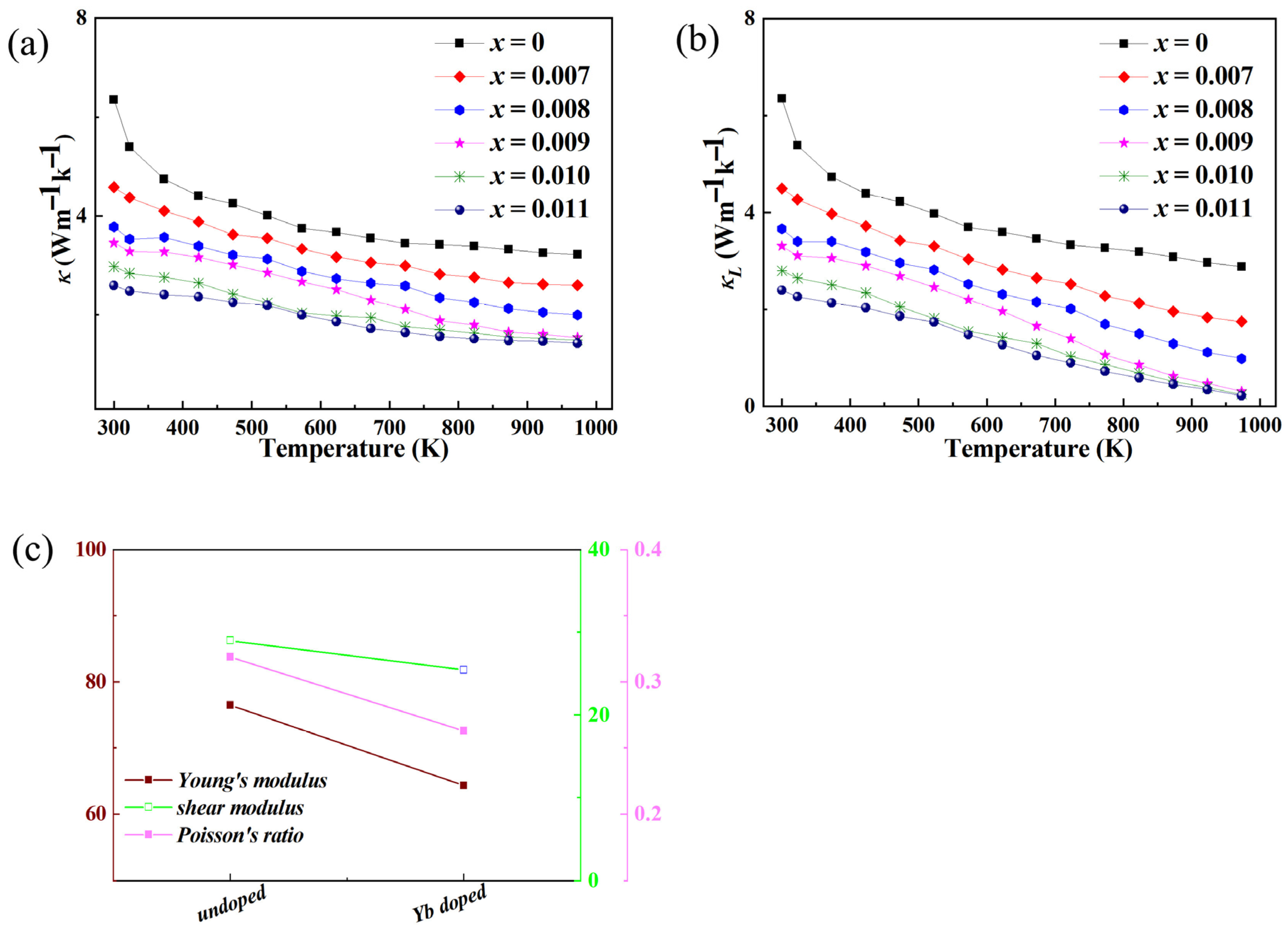
Figure 6 illustrates the temperature-dependent thermal conductivity of Yb
2O
3-doped In
2O
3-based thermoelectric materials in the temperature range of 300–800 °C. It is clearly observed that the total thermal conductivity (κ) of all samples decreases with increasing temperature. This trend is primarily attributed to enhanced phonon-phonon scattering (Umklapp scattering) at elevated temperatures. More importantly, compared to the pristine, undoped In
2O
3 sample, all Yb
2O
3-doped samples exhibit a significantly reduced thermal conductivity across the entire temperature range. This result indicates that the introduction of Yb
2O
3 is an effective strategy for lowering the thermal conductivity of In
2O
3-based materials. The total thermal conductivity (κ) is composed of two main contributions: the carrier thermal conductivity (κ
e) and the lattice thermal conductivity (κ
1), following the relationship κ = κ
e + κ
1. To gain a deeper understanding of the intrinsic mechanism behind the reduction in thermal conductivity, it is essential to decouple these two components. According to the Wiedemann–Franz law, the carrier thermal conductivity (κ
e) can be estimated using the equation κ
e = LσT, where L is the Lorenz number, σ is the electrical conductivity, and T is the absolute temperature. As previously discussed, Yb
2O
3 doping significantly enhances the electrical conductivity (σ) of the material, which would typically lead to an increase in κ
e. However, calculation results reveal that although κ
e increases, its contribution to the total thermal conductivity remains relatively minor. Therefore, the significant decrease in the total thermal conductivity must originate from a substantial reduction in the lattice thermal conductivity (κ
1). The reduction in lattice thermal conductivity is primarily attributed to the enhancement of phonon scattering. In crystalline materials, heat is predominantly transported by lattice vibrations, or phonons. Any microstructural features that impede the propagation of phonons will reduce κ
1. Point defect scattering is the central reason for the decrease in κ
1. When Yb
3+ ions (with an ionic radius of approximately 0.868 Å) substitute for In
3+ ions (with an ionic radius of approximately 0.800 Å) in the In
2O
3 lattice, local strain fields and mass fluctuations are created due to the differences in mass and radius between the two ions. These point defects act as potent scattering centers for phonons with short-to-medium wavelengths [
19,
20]. According to point defect scattering theory, the scattering intensity is proportional to the square of the mass and radius differences between the dopant and host atoms. Consequently, Yb
2O
3 doping effectively disrupts the periodicity of the crystal lattice, shortens the phonon mean free path, and thus significantly lowers the lattice thermal conductivity.
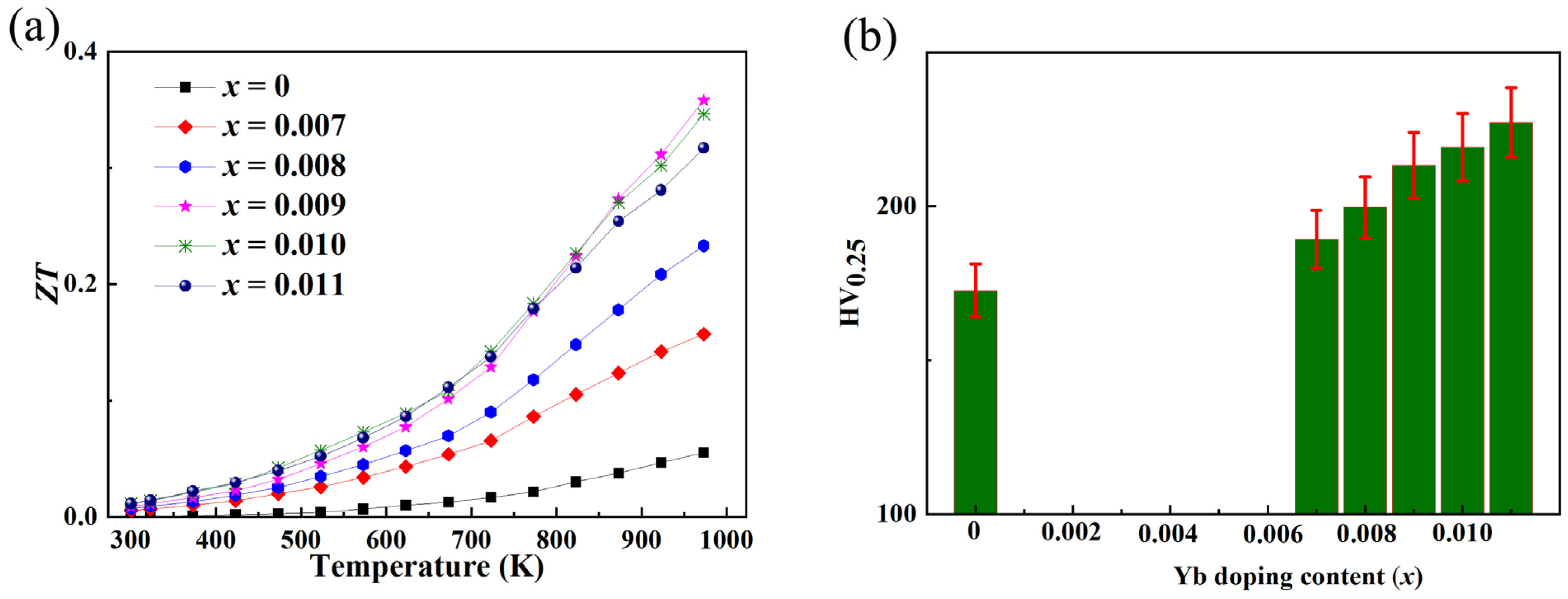
There was a significant improvement in ZT value, with the highest value of 0.358 (923 K) in Yb
2O
3-doped In
2O
3, as shown in
Figure 7a, higher than ~0.18 for Ge doping but lower than ~0.42 for V doping, which is the highest
ZT value for In
2O
3 [
21,
22]. The elevated power factor acts as the dominant driving force for the improved ZT value in Yb
2O
3-doped In
2O
3. Doping-generated oxygen vacancies act as effective donors, remarkably boosting carrier concentration. Despite slightly reduced mobility caused by lattice distortion, the pronounced increase in carrier concentration predominates to enhance electrical conductivity. Meanwhile, the narrowed band gap and increased density of states near the Fermi level optimize electronic transport, further reinforcing conductivity. Although the Seebeck coefficient decreases moderately with high carrier concentration, the notably enhanced electrical conductivity overwhelms this negative effect, leading to a distinctly improved power factor. The suppressed total thermal conductivity provides crucial synergy for ZT enhancement. Lattice distortion, oxygen vacancies and dopant ions collectively introduce intensive phonon scattering centers, shortening the phonon mean free path and depressing lattice thermal conductivity significantly. Even though electronic thermal conductivity rises slightly, the dominant reduction in lattice thermal conductivity ensures an overall decrease in total thermal conductivity. Yb
2O
3 doping realizes synergistic optimization of electronic and thermal transport via defect and electronic structure engineering. This dual optimization synchronously elevates the power factor and reduces thermal conductivity, contributing to a remarkable ZT enhancement, which offers an insightful strategy for designing high-performance oxide thermoelectric materials.
The pronounced enhancement in Vickers hardness of In
2O
3 upon Yb
2O
3 doping, as shown in
Figure 7b, arises from a synergistic mechanism integrating lattice distortion strengthening, multi-defect synergistic regulation, and electronic bonding reconstruction, which establishes an intrinsic correlation between mechanical reinforcement and thermoelectric transport optimization. The Vickers hardness reaches a maximum of 227.25 HV. From the viewpoint of lattice structural evolution, the ionic radius mismatch between Yb
3+ and In
3+ drives local lattice distortion upon substitutional solid solution formation. The generated internal stress field disrupts the perfect lattice integrity and impedes dislocation migration, raising the critical stress for plastic deformation and elevating hardness effectively. Meanwhile, the distorted lattice refines atomic packing density, reinforcing resistance against external mechanical loading. Defect engineering serves as a core contributor to hardness enhancement. Yb doping induces the formation of substitutional defects and oxygen vacancies, constructing a multi-scale defect system that creates intensive energy barriers against atomic slip and rearrangement. Uniformly dispersed defects avoid localized stress concentration, ensuring homogeneous mechanical reinforcement. Notably, such defect configuration also optimizes carrier transport behavior, enabling a direct synergy between mechanical robustness and electrical transport properties. At the electronic scale, the discrepancy in electronegativity between Yb and In atoms enhances the covalent character of Yb–O bonds compared with In–O bonds, strengthening interatomic cohesion and resistance to deformation. Moreover, doping-induced electronic structure evolution, including band structure modulation and elevated density of states near the Fermi level, reflects the redistribution of valence electrons. This electronic reconstruction reinforces interatomic interactions and improves microstructural stability, macroscopically manifesting as enhanced hardness. This work reveals a multi-scale strengthening mechanism spanning lattice distortion, defect regulation, and electronic interaction reconstruction, which not only elucidates the fundamental origin of hardness improvement but also bridges mechanical properties and thermoelectric transport. Such an integrated mechanism provides a novel theoretical paradigm for designing high-performance thermoelectric ceramics with balanced mechanical and functional properties.
3. Experimental Part
Indium oxide (In2O3, 99.99%, Sinopharm Chemical Reagent Co., Ltd., Shanghai, China) and ytterbium oxide (Yb2O3, 99.99%, Sinopharm Chemical Reagent Co., Ltd.) were employed as precursor constituents to synthesize ytterbium-doped indium oxide bulk specimens. The starting reagents were accurately massed within an inert atmosphere glove-box and subsequently transferred into a zirconia milling jar. The vessel was sealed and backfilled with high-purity argon gas to safeguard against oxidation. Mechanical alloying was initially executed at a rotation speed of 400 revolutions per minute for a duration of 12 h. Following this primary step, anhydrous ethanol was introduced as a process control agent, and a secondary low-speed milling cycle was implemented for 1 h to ensure homogeneous mixing. The resulting slurry was then extracted and subjected to 48 h of vacuum drying to yield homogeneous oxide powder precursors. The consolidation protocol for bulk sintering proceeded as delineated below: The as-prepared powder was loaded into a high-density graphite die, which was subsequently positioned inside a spark plasma sintering (SPS) chamber. The furnace was evacuated to a high vacuum and subsequently purged with argon gas to establish an inert thermal treatment environment. The sample was heated to a target temperature of 1273 Kelvin at a rapid ramp rate of 50 Kelvin per minute, held isothermally for 60 min to ensure uniform densification, and finally cooled to room temperature at the same cooling rate. The pressure during the heat preservation stage is 60 MPa. This process yielded dense, cylindrical bulk pellets suitable for subsequent property evaluations. The multi-dimensional characterization framework adopted to assess the synthesized materials included the following four key facets.
Crystal Structure Analysis: Phase purity and secondary phase formation were characterized using X-ray diffraction (XRD) on a Bruker AXS D8 diffractometer. Data were collected using monochromatic Cu Kα radiation (λ = 1.5406 Å) over a 2θ range from 10° to 80°, with a step size of 0.20°, operating at a tube current of 20 mA and an acceleration voltage of 40 kV.
Electrical Transport Properties: The thermoelectric performance, specifically the Seebeck coefficient and electrical conductivity, was measured using a ZEM-3 system (Ulvac-Riko, Yokohama, Japan) to quantify the power factor variation induced by ytterbium doping.
Carrier Transport Parameters: Hall effect measurements were conducted on an Ekopia HMS-5500 system (Ecopia Corporation, Anyang City, South Korea) to determine the carrier concentration and mobility, thereby elucidating the underlying electron transport mechanisms. Hall effect measurements were performed at room temperature (300 K).
Thermal Transport Properties: Thermal conductivity components, including thermal diffusivity and specific heat capacity, were characterized using a NETZSCH LFA457 laser flash analyzer (NETZSCH-Gerätebau, Selb, Germany)to evaluate the thermal transport behavior.
First-principles density functional theory (DFT) calculations were carried out utilizing the CASTEP code embedded in the Materials Studio 8.0 software package. The plane-wave basis set was truncated at an energy cutoff of 550 eV to ensure convergence. The total energy was minimized until the residual force on each atom was less than 0.05 eV/Å, and the total energy change converged to below 2.0 × 10⁻⁵ eV per atom. The self-consistent field (SCF) iteration was executed with an energy tolerance of 10−6 eV per atom. The structural models employed in the DFT calculations were constructed based on the cubic bixbyite structure of In2O3, which belongs to the space group Ia-3 (No. 206). The optimized equilibrium lattice parameter of pure In2O3 was determined to be 1.0117 nm (10.117 Å). To simulate Yb-doped In2O3, a 2 × 2 × 1 supercell was built from the primitive unit cell. Yb dopants were introduced by substituting In3+ sites with Yb3+ ions at the Wyckoff positions 8b and 24d in the Ia-3 structure, while maintaining overall charge neutrality. The atomic coordinates of In, O, and substitutional Yb atoms were fully relaxed during the geometry optimization.
The bulk densities of the as-sintered samples were measured via the Archimedes’ method using distilled water as the immersion medium. The relative densities, calculated as the ratio of the measured bulk density to the theoretical density of the In2O3-based matrix, were determined to be 97.13%, 97.22%, 97.31%, 97.29%, 97.23%, and 97.25% for the compositions with Yb doping contents x = 0, 0.007, 0.008, 0.009, 0.010, and 0.011, respectively. The experimental uncertainties associated with the thermoelectric measurements were rigorously quantified: the combined uncertainty for the Seebeck coefficient and electrical conductivity was determined to be 5%. For thermal conductivity, after accounting for the errors in thermal diffusivity, specific heat capacity, and sample density, the estimated uncertainty was maintained within 8%. Consequently, the overall combined uncertainty for the figure-of-merit (ZT) calculations was calculated to be less than 15%. All bulk samples were mechanically processed to obtain two parallel, flat surfaces. The central region of each pellet was selected for Vickers hardness (HV) testing to ensure representativeness. Hardness measurements were performed on an HV-1000 microhardness tester under a static load of 25 g-force for a dwell time of 15 s. Five discrete indents were made per sample, and the average HV value was computed to characterize the material’s mechanical robustness.