Article

Electrical and Electronic Quality Improvement of Multicrystalline Silicon Solar Cells via Hydrogen Plasma Treatment


1
Nanomaterials and Systems for Renewable Energy Laboratory, Research and Technology Center of Energy, Technoparc Borj Cedria, BP 095, Hammam Lif 2050, Tunisia
2
Universite de Tunis el Manar, BP 94, Rommana, Tunis 1068, Tunisia
3
College of Engineering, Imam Mohammad Ibn Saud Islamic University (IMSIU), Riyadh 11432, Saudi Arabia
*
Author to whom correspondence should be addressed.
Inorganics 2026, 14(4), 105; https://doi.org/10.3390/inorganics14040105
Submission received: 5 February 2026 / Revised: 17 February 2026 / Accepted: 25 February 2026 / Published: 7 April 2026
(This article belongs to the Special Issue New Semiconductor Materials for Energy Conversion, 2nd Edition)

Abstract

In this work, the impact of hydrogen plasma treatment on the electrical and electronic quality of multicrystalline silicon (mc-Si) was systematically investigated using plasma-enhanced chemical vapor deposition (PE-CVD). Hydrogen radicals generated in the plasma effectively passivate dangling bonds, reducing electrically active defects and enhancing material quality. Optimized PE-CVD conditions were applied to promote efficient hydrogen incorporation and surface modification. Optical characterization, including reflectivity measurements and FT-IR spectroscopy, confirms the formation of Si–H bonds and a significant reduction in surface reflectivity of up to 66% at 600 nm. Electrical and optoelectronic analyses reveal pronounced improvements in carrier lifetime and diffusion length, increased by 200% and 79%, respectively. In addition, dark current–voltage (I–V) measurements show a 32% decrease in series resistance and a 51% increase in shunt resistance, indicating enhanced charge transport and suppressed leakage currents. These macroscopic electrical improvements are supported by light beam-induced current (LBIC) measurements, which demonstrate a 14% increase in grain boundary current, confirming effective hydrogen passivation and reduced recombination. Overall, hydrogen plasma PE-CVD treatment is shown to significantly improve the electronic quality and photovoltaic performance of mc-Si solar cells.

1. Introduction

The continuous increase in global energy demand, coupled with the urgent need to mitigate carbon emissions, has positioned solar photovoltaics (PV) as a key technology for sustainable energy generation [1,2,3]. mc-Si dominates the PV market [4,5], accounting for nearly 90% of production, due to its reliability, relatively low manufacturing cost, and long operational lifetime of up to 30 years. This material offers an effective compromise between module efficiency (≈12–20%) and cost, making it particularly suitable for large-scale solar energy deployment [6,7,8,9].
Solar cell technologies employ a wide range of materials for light absorption, charge transport, passivation, and optical management. Binary oxide ceramics such as TiO2, ZnO, Al2O3, SiO2, CeO2, Fe2O3, and WO3 have been widely investigated for photovoltaic applications [10]. In addition, material optimization and defect engineering are key factors for improving efficiency and sustainability in photovoltaic systems [11]. Despite advances in emerging materials, mc-Si remains a dominant and cost-effective absorber material. Therefore, improving its properties through hydrogen plasma passivation is important for enhancing solar cell performance.
Despite its widespread use, the performance of mc-Si is fundamentally constrained by structural and chemical defects. Grain boundaries, dislocations, stacking faults, and residual metallic impurities act as highly efficient recombination centers [12,13,14,15,16,17,18]. These defects reduce minority carrier lifetime and diffusion length, limiting photovoltaic conversion efficiency. Grain boundaries create electrostatic barriers that hinder charge transport, while metallic impurities and dangling bonds introduce deep-level traps that accelerate non-radiative recombination. Minimizing these defects is therefore critical to improving device performance. Surface and bulk passivation techniques are widely employed to chemically neutralize electrically active defects, reduce surface recombination velocity, and enhance carrier lifetime [19,20,21].
Recent advances in photovoltaic (PV) technology have highlighted the importance of improving the optical, electrical, and optoelectronic properties of multicrystalline silicon wafers through the combined management of bulk defects and surface states [19,22,23,24]. Gettering is a well-established purification technique that enhances the electronic quality of silicon by removing metallic impurities from the electrically active region and redistributing them to designated sink sites. Conventional gettering methods, including phosphorus diffusion [20], aluminum-assisted gettering [25], and silicon nitride-based gettering [26,27], are typically implemented during high-temperature thermal treatments. While these processes effectively improve carrier transport and lifetime, their ability to eliminate nanoscale defects remains limited, particularly at grain boundaries and in regions containing residual metal precipitates. Therefore, supplementary post-treatment strategies are required to further reduce defect-induced recombination.
High defect densities in mc-Si are known to reduce carrier lifetime and device efficiency. These defects are effectively passivated by hydrogen through the neutralization of dangling bonds and recombination centers. Hydrogen plasma passivation using PE-CVD has been demonstrated to be an effective approach for addressing these limitations [28,29,30].
PE-CVD has been widely applied to enhance the performance of low-temperature a-SiGe:H thin-film transistors [31] and to study the influence of radio-frequency power on the structural, optical, and electronic properties of microcrystalline silicon (μc-Si:H) films [32].
This study analytically investigates the impact of hydrogen plasma treatment on the morphological, optical, electrical and electronic properties of mc-Si substrates. A comprehensive experimental approach is employed, including Fourier-transform infrared (FT-IR) spectroscopy to confirm Si–H bond formation, reflectivity measurements to assess optical performance, carrier lifetime and diffusion length evaluations to quantify electronic quality, profilometry to characterize surface morphology and the electrical parameters extracted from the dark current–voltage (I–V) characteristics and well supported by the spatially resolved light beam-induced current (LBIC) measurements. The integration of these techniques enables a thorough assessment of passivation effectiveness and provides guidance for optimizing processing parameters to achieve high-performance mc-Si photovoltaic devices.

2. Results and Discussions

In this study, a comprehensive characterization of the hydrogen plasma treatment applied using the PE-CVD reactor [28] to passivate the surface and bulk of the mc-Si was conducted. The investigation covered electronic properties (minority carrier lifetime and diffusion length), optical properties using Fourier Transform Infrared Spectroscopy (Nicolet MAGNA-IR 560 ESP FT-IR, Madison, WI, USA) and UV–Visible spectroscopy (Perkin-Elmer Lambda 950, Springfield, IL, USA), and surface morphology using profilometry and electrical characterizations by light beam-induced current (LBIC) and dark current–voltage (I–V).
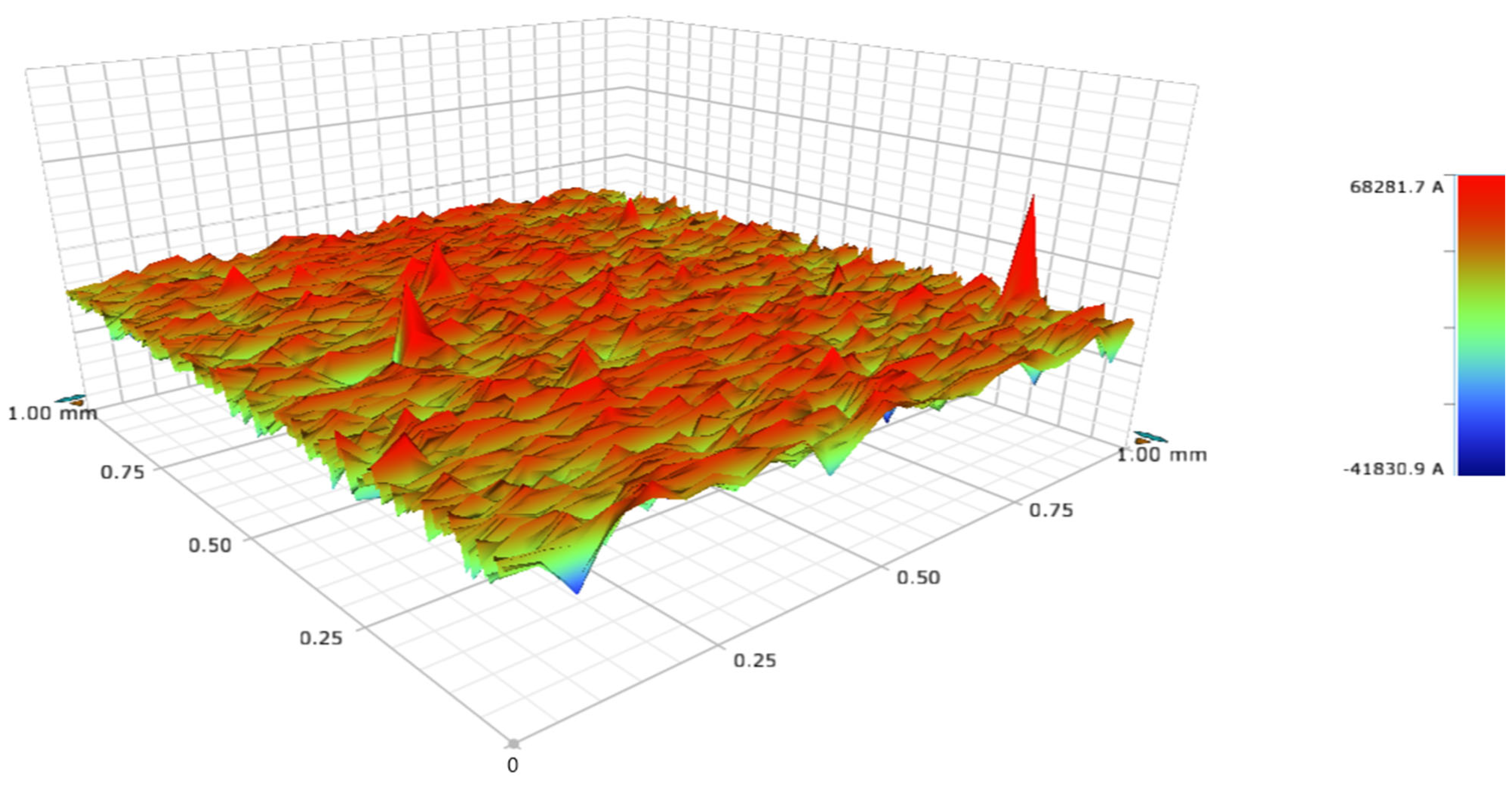
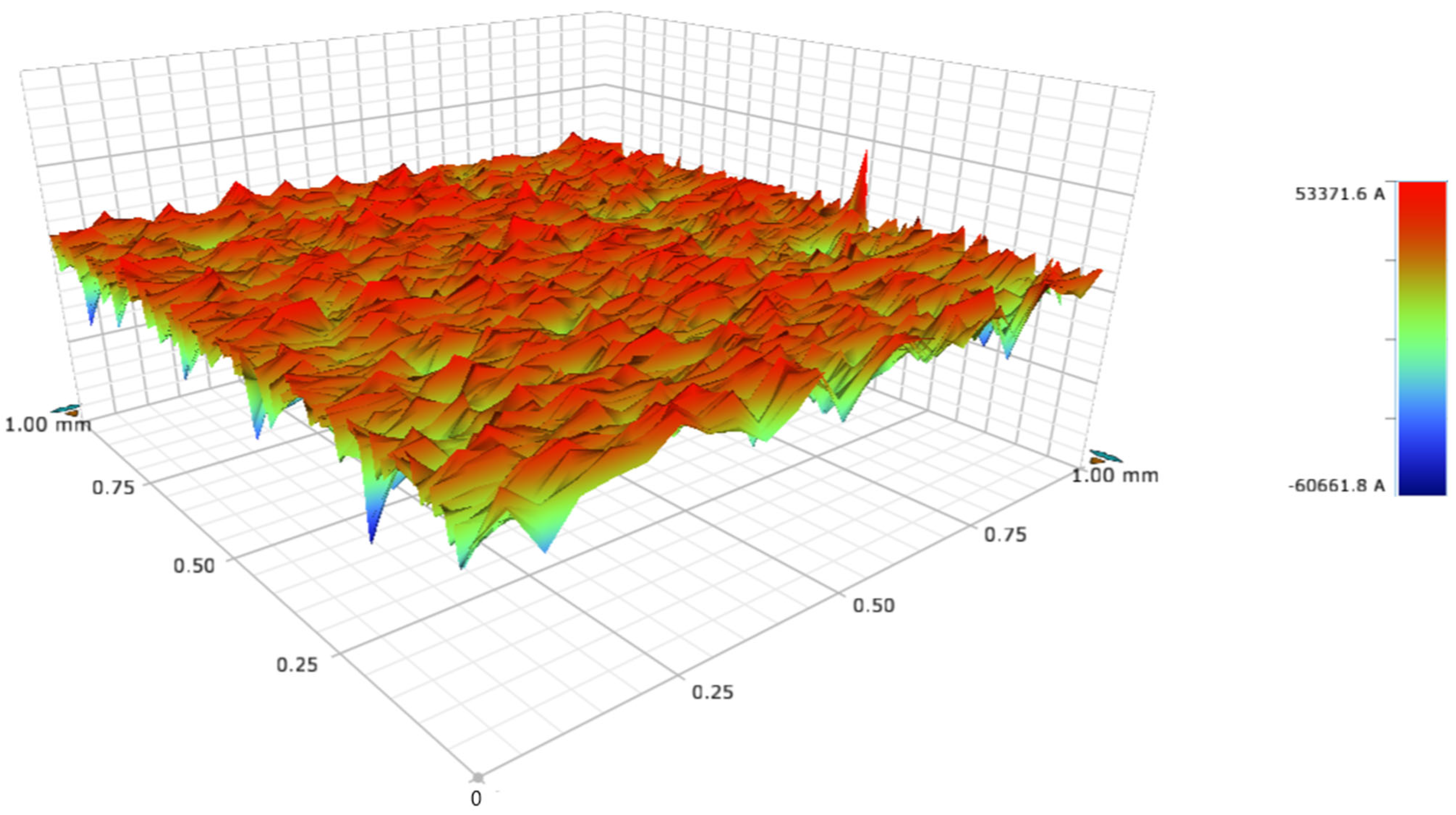
The morphology study of the multicrystalline silicon (mc-Si) surface, mapped using 3D roughness profilometry, reveals significant variations based on the applied chemical and plasma treatments. The 3D roughness profilometry characterization was performed after hydrogen plasma treatment via PE-CVD on mc-Si substrates in an area of 2 × 2 cm2, which is shown in Figure 1. From these measurements, we extracted the root-mean-square (RMS) roughness values, which are included in Table 1.
The increase in surface roughness after mc-Si treatment is beneficial for photovoltaic devices, as the resulting texturing enhances light trapping by scattering and redirecting incident photons, reducing direct reflection [33].
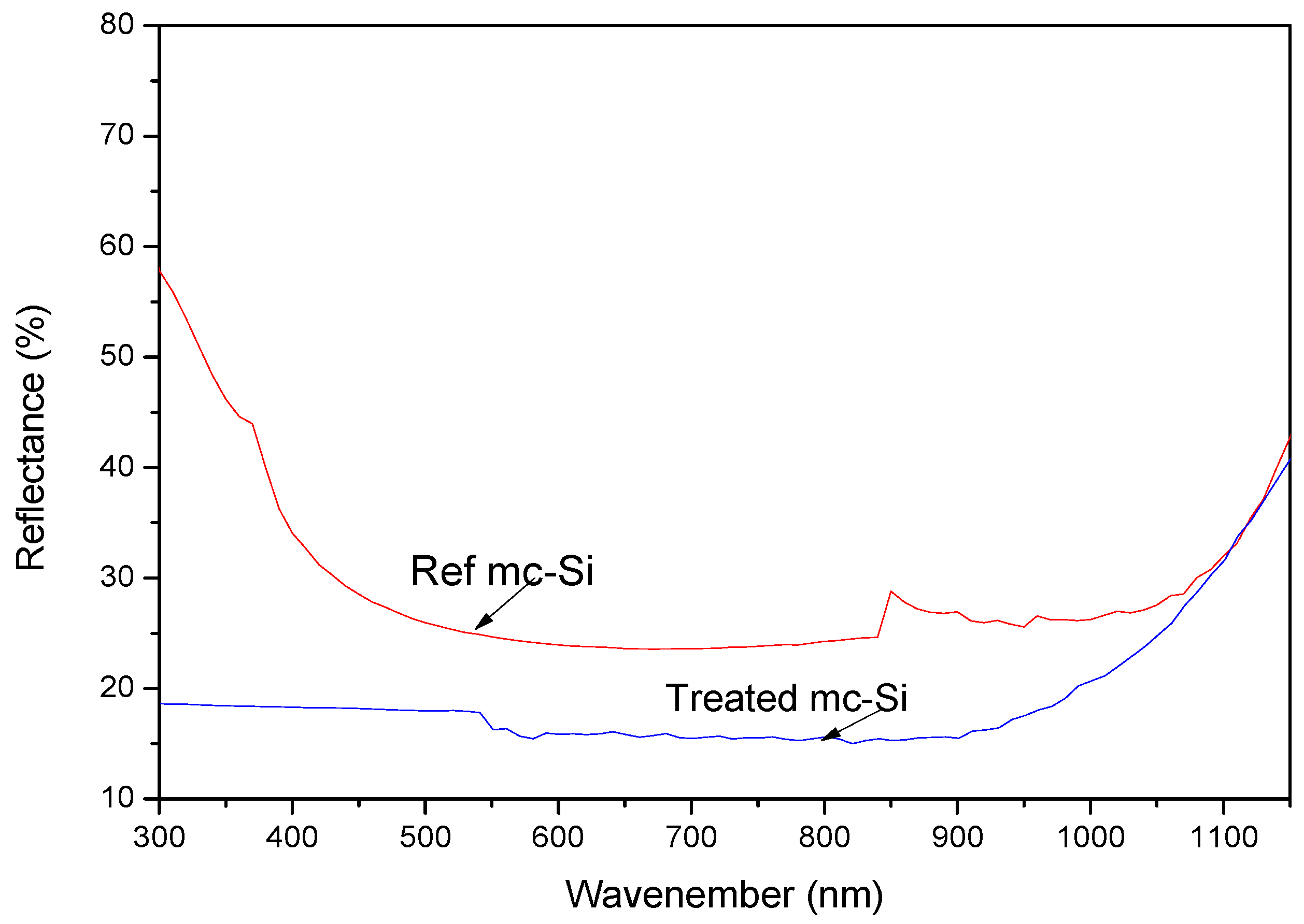
Figure 2 shows the reflectivity spectra of multicrystalline silicon (mc-Si) before and after hydrogen plasma treatment. All reported values correspond to the average reflectance measured over the 400–800 nm wavelength range, at normal incidence, using an integrating sphere. The figure highlights the effect of the treatment on the total reflectivity. It is observed that after H2 plasma treatment on the cleaned mc-Si sample, the reflectivity decreases significantly across the 400–800 nm wavelength range, reaching approximately 15%, compared to 26% for the reference sample, demonstrating a substantial reduction in the surface reflectivity.
This result proves to be more effective than that obtained with the NaOH treatment alone [34]. This reduction is mainly explained by the fact that this treatment induces surface roughness, which influences the porosity of the formed layer.
Untreated mc-Si contains the intrinsic vibrational features of the silicon lattice and any native oxide. By using it as the background, these inherent contributions are subtracted, allowing the FT-IR spectrum to highlight only the changes introduced by the H2 plasma PE-CVD treatment.
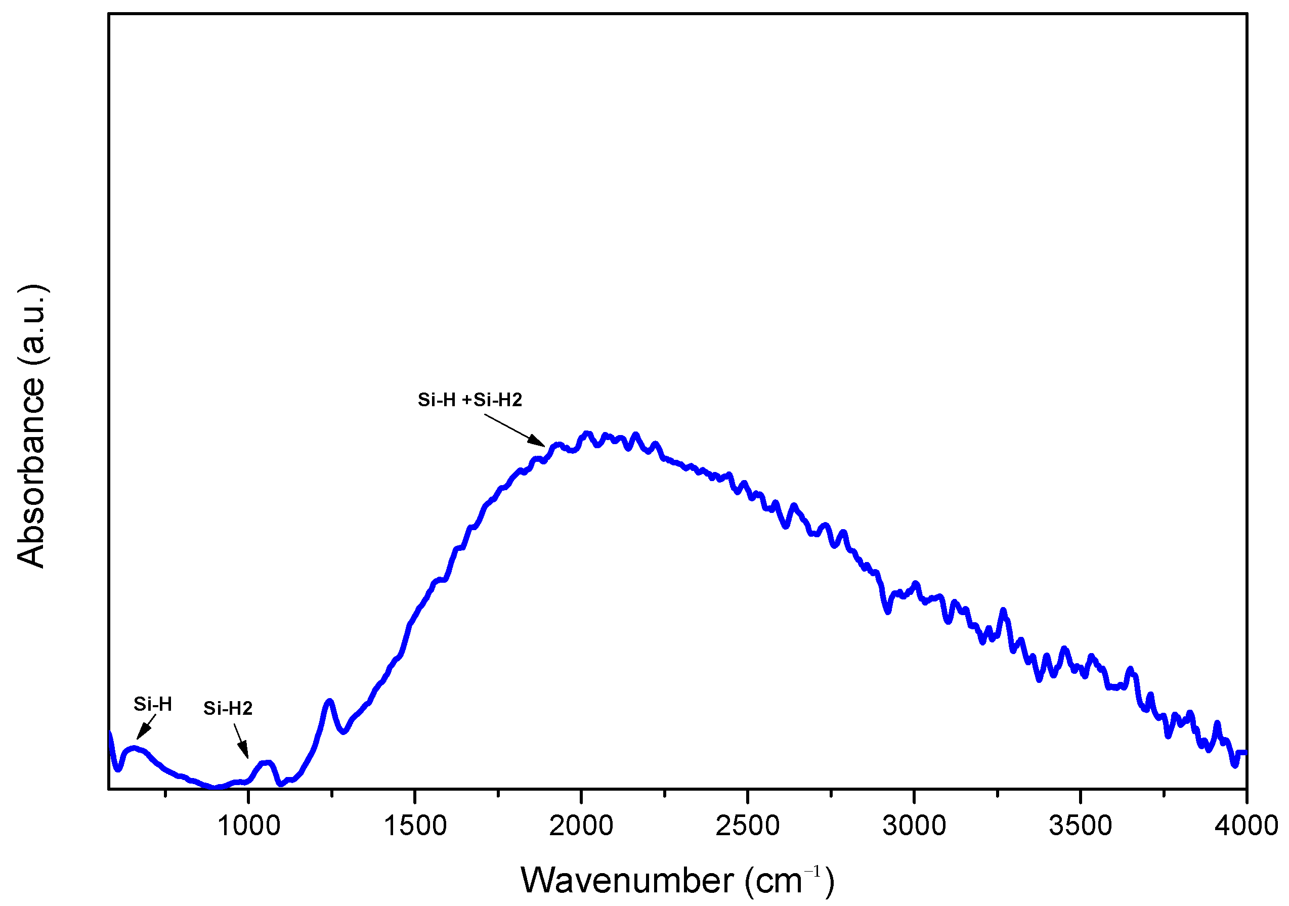
Figure 3 presents the FT-IR spectra of multicrystalline silicon after H2 plasma PE-CVD treatment performed in transmission mode on mc-Si wafer pieces, highlighting the chemical bonding modifications induced by hydrogenation. In our experimental procedure, the untreated multicrystalline silicon (mc-Si) sample was used as background reference for the FT-IR measurements. As a result, the presented FT-IR spectrum corresponds to the hydrogen plasma-treated sample normalized against the untreated substrate. This approach allows us to eliminate intrinsic silicon absorption contributions and highlight only the vibrational modes introduced by the hydrogen plasma treatment. In contrast, the H2 plasma-treated mc-Si sample shows a pronounced increase in absorbance intensity and the emergence of distinct vibrational bands characteristic of hydrogen bonding configurations.
A strong absorption band observed in the 600–640 cm−1 region is attributed to Si–H wagging and bending modes [35], providing direct evidence of hydrogen incorporation into the silicon network. Additional absorption features appearing near 900–1050 cm−1 are associated with Si–H2 bonding configurations [36,37], which are commonly linked to the effective passivation of extended defects and grain boundaries.
Also, after hydrogen plasma treatment, a broad band is observed in the 1500–3500 cm−1 spectral range, which is attributed to the convolution of two vibrational modes: Si–H and Si–H2 [38,39].
The emergence and enhanced intensity of Si–H- and Si–H2-related bands after H2 plasma treatment confirm the efficient hydrogen passivation of dangling bonds and electrically active defect states within the grains and at grain boundaries [40]. Such hydrogen–silicon interactions are widely associated with the passivation of electrically active defects, especially dangling bonds at the surface and grain boundaries, which can contribute to improved electronic and optical properties of the material.
Hydrogen plasma treatment on mc-Si leads to a substantial reduction in recombination-active centers, in good agreement with the significant improvement in effective carrier lifetime observed in the lifetime mapping and histogram analyses. Overall, the FT-IR results substantiate the critical role of H2 plasma PE-CVD treatment in modifying the bonding structure of multicrystalline silicon and in enhancing its electronic quality through effective defect and interface passivation.
Spatial mappings of the effective carrier lifetime and the minority carrier diffusion length were carried out using the WT2000 system before and after treatment in order to assess the impact of H2 plasma on the electronic quality of the mc-Si wafer.
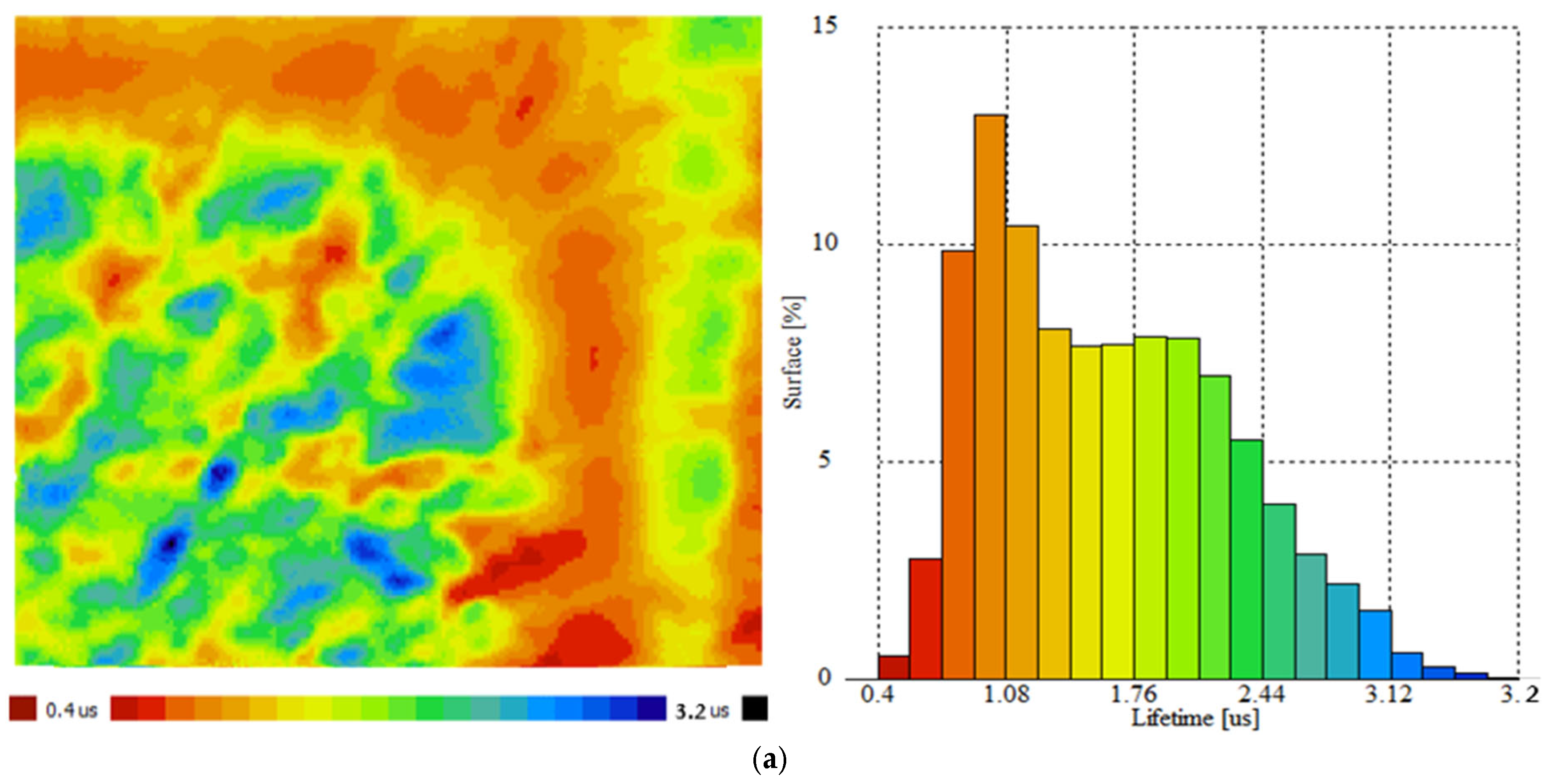
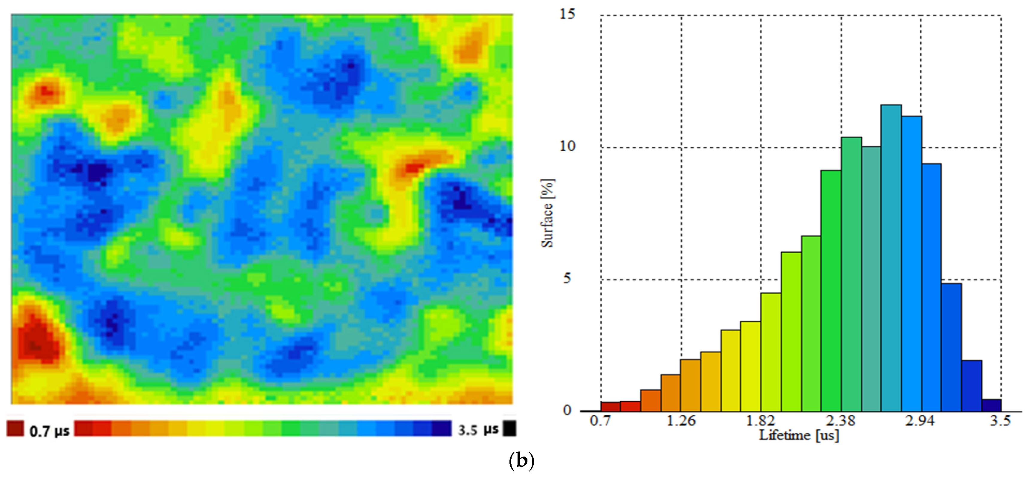
The maps and histograms of effective carrier lifetime before and after H2 treatments are presented in Figure 4. In these maps, red regions correspond to the lowest lifetimes, whereas blue regions represent the highest lifetimes. Prior to treatment (Figure 4a), carrier lifetimes exhibit a broad distribution with a dominant peak around ~1 µs, accompanied by a significant fraction of low-lifetime regions, which are predominantly associated with high recombination activity at grain boundaries and defect-rich areas. The lifetime mappings and histograms shown in Figure 4b further illustrate a pronounced enhancement in the electronic quality of multicrystalline silicon after H2 plasma PE-CVD treatment. Following H2 plasma treatment, as depicted in Figure 4b, the lifetime distribution shifts substantially toward longer values, with a new peak centered at approximately 2.6–2.9 µs. Simultaneously, low-lifetime regions are markedly suppressed, and the overall distribution becomes narrower and more homogeneous across the wafer. These observations indicate the effective hydrogen passivation of dangling bonds and electrically active defects both within grains and at grain boundaries, leading to a pronounced reduction in bulk and interfacial recombination. Generally, the treatment results in an approximate 2–3 fold increase in effective carrier lifetime, highlighting the efficacy of H2 plasma PE-CVD as a post-treatment approach for significantly improving the electronic properties of multicrystalline silicon.
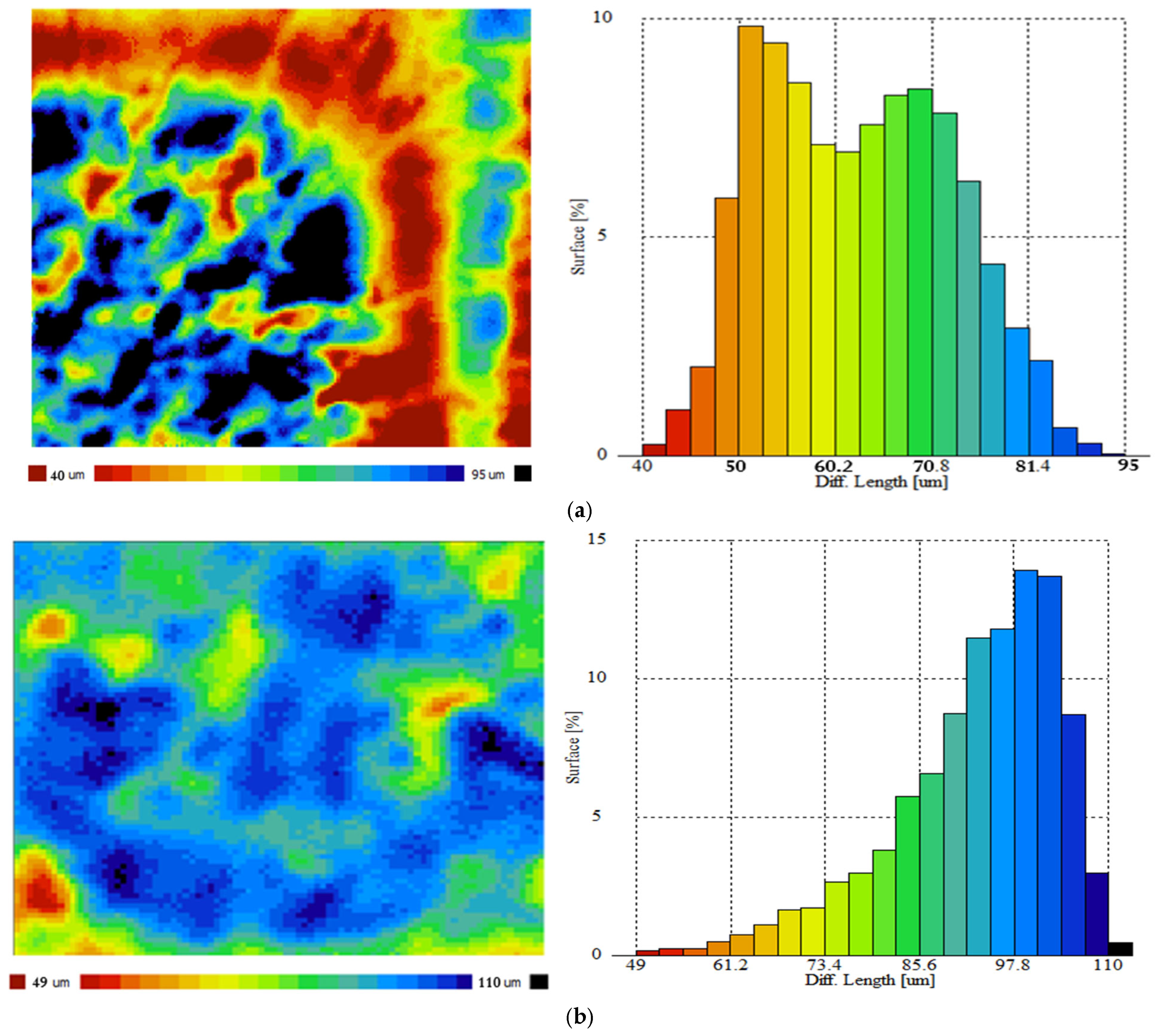
The mappings shown in Figure 5 reveal the spatial distribution of the diffusion length of mc-Si wafers. For the reference sample, the diffusion length values range from 40 µm to 95 µm. As illustrated in Figure 5a, a clear improvement in diffusion length is observed after H2 treatment, with the blue regions corresponding to the highest diffusion lengths dominating most of the wafer surface, while the lowest values are mainly located at the edges. Following the treatment, a significant enhancement in the diffusion length is achieved, with values extending from 49 µm to 110 µm, accompanied by a notable improvement in the edge regions.
Before H2 treatment, as shown in Figure 5a, the histogram of the diffusion length distribution is relatively broad and dominated by shorter values, with most of the surface contribution lying between approximately 55 and 75 µm and a noticeable tail extending toward smaller diffusion lengths. This behavior indicates significant carrier recombination and pronounces spatial heterogeneity across the surface. After H2 treatment, as shown in Figure 5b, the entire histogram distribution shifts toward higher diffusion lengths, extending up to ~110 µm, with a pronounced maximum in the 90–100 µm range and a strong reduction in the population of low diffusion lengths. This evolution reflects a substantial increase in both the mean and effective diffusion length, along with improved surface uniformity. The observed enhancement is consistent with the hydrogen-induced passivation of defects and trap states, which reduces non-radiative recombination and increases the carrier lifetime [28], as demonstrated in Figure 4b, ultimately leading to longer carrier diffusion lengths throughout the material.
Dark current–voltage (I–V) measurements are a powerful tool for evaluating junction quality and identifying internal electrical losses in solar cells. In particular, the series resistance (Rs) and shunt resistance (Rsh) play a critical role in determining device performance. The series resistance originates from charge transport limitations within the bulk material, metal–semiconductor contacts, and interconnection layers; An increase in Rs results in higher resistive losses, consequently, degraded solar cell performance. In contrast, the shunt resistance is associated with parasitic leakage pathways arising from structural defects or poor interface quality, and a low Rsh results in increased leakage current at low bias, thereby reducing overall device efficiency.
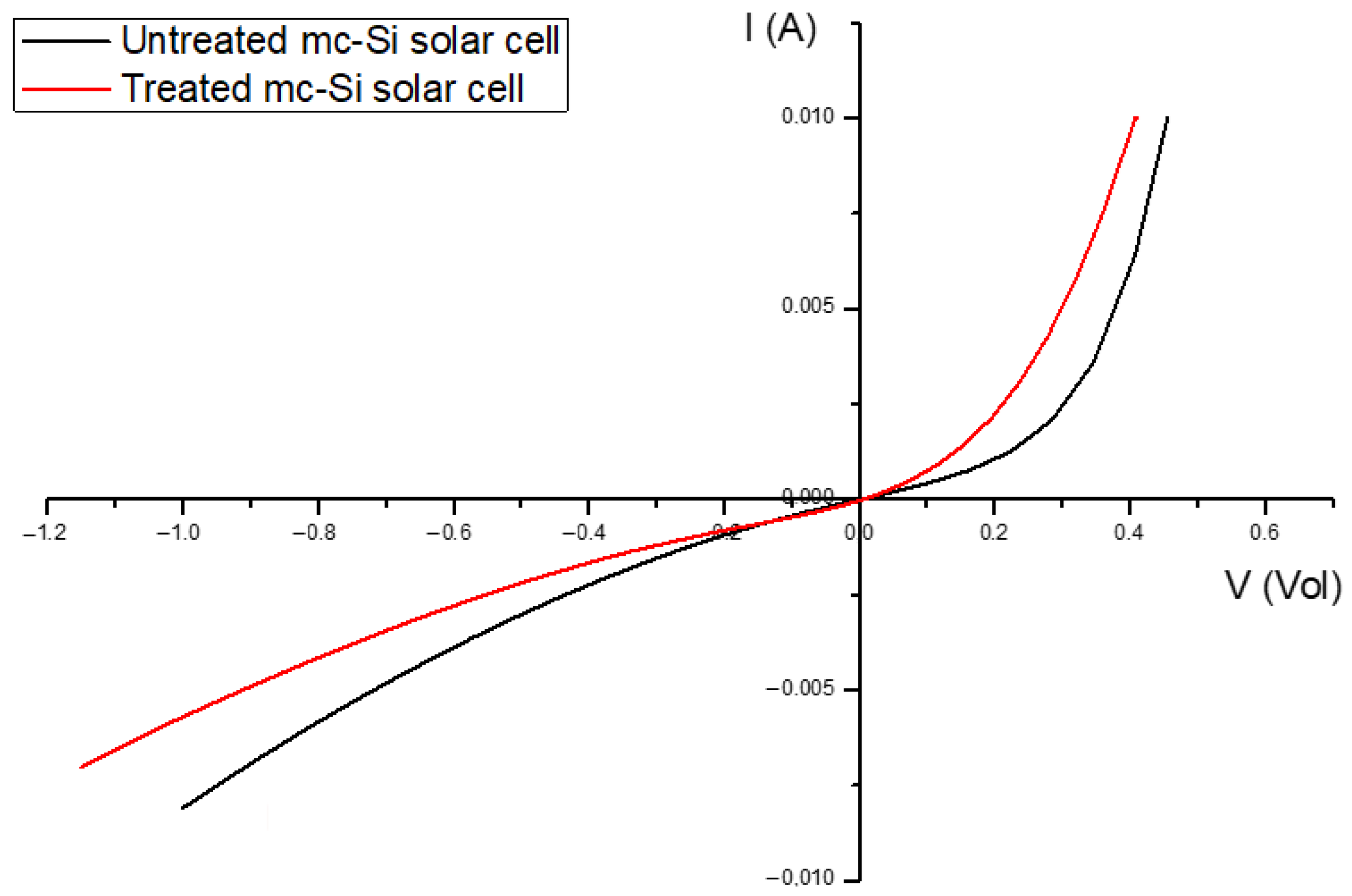
In dark I–V characteristics, Rs primarily affects the high-bias region where the response becomes Ohmic, whereas Rsh governs the near-zero-bias region where deviations from ideal diode behavior are most pronounced. In this work, Rs and Rsh were extracted using a differential method based on the dV/dI technique: Rs was estimated from the high-current region where the I–V curve becomes linear (Rs ≈ dV/dI), while Rsh was derived from the near-zero-bias region (Rsh ≈ V/I). Analysis of the dark I–V characteristics before and after hydrogen plasma treatment, as shown in Figure 6, reveals a clear improvement in the electrical performance. Following treatment, the series resistance decreases from 19 Ω to 13 Ω, corresponding to an improvement of approximately 32%, indicating enhanced carrier transport and reduced contact resistance. Simultaneously, the shunt resistance increases from 166 Ω to 250 Ω, representing an improvement of about 51%, which reflects the effective suppression of leakage currents due to defect passivation at the surface and grain boundaries [41]. These results demonstrate that H2 plasma PE-CVD treatment significantly improves the electrical quality of mc-Si solar cells, as shown in Table 2.
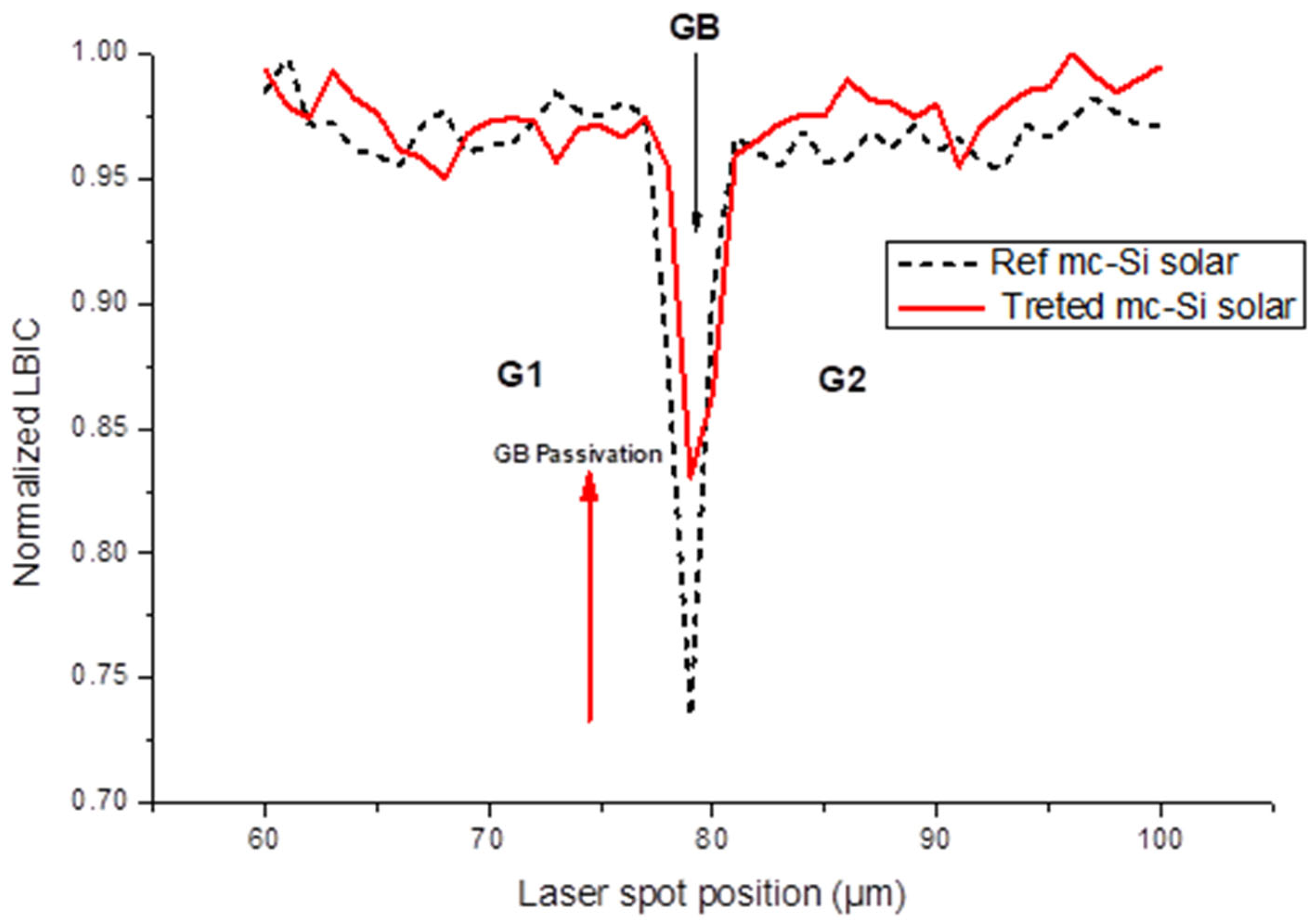
To qualitatively evaluate grain boundary-related defects in multicrystalline silicon (mc-Si) solar cells before and after hydrogen treatment, light beam-induced current (LBIC) measurements were performed using a He–Ne laser source with a wavelength of 633 nm and a maximum output power of 5 mW. At this wavelength, the optical penetration depth in silicon is approximately 2–3 µm, meaning that carrier generation occurs primarily near the surface region. This technique enables spatially resolved analysis of local carrier collection efficiency and recombination activity associated with microstructural features such as grain boundaries.
Figure 7 presents the normalized LBIC profiles measured across two adjacent grains (G1 and G2) and the intervening grain boundary (GB) in an mc-Si solar cell before and after hydrogen treatment. In the untreated sample, a pronounced reduction in the LBIC signal is observed at the grain boundary, where the normalized current reaches a value of approximately 0.73, indicating strong carrier recombination associated with defect-rich GB regions. After hydrogen treatment (red curve), the LBIC signal at the grain boundary increases to about 0.83, corresponding to an improvement of approximately 14%. The reduced current contrast at the grain boundaries demonstrates effective hydrogen passivation of electrically active defects [42], leading to suppressed recombination losses and enhanced carrier collection efficiency. These results provide direct evidence that hydrogen treatment improves the electronic quality of multicrystalline silicon by mitigating grain boundary recombination [43].
Quantitatively, as summarized in Table 3, the H2 treatment reduces reflectivity from 24% to 15% (60% improvement), increases the maximum diffusion length from 56 µm to 100 µm (79% enhancement), and raises the maximum carrier lifetime from 1 µs to 3 µs (200% enhancement). Together, these results demonstrate that H2 plasma treatment effectively enhances both the optical and electronic properties of mc-Si wafers. The improvements observed in the electrical parameters extracted from the dark I–V characteristics are well supported by the spatially resolved LBIC measurements. After hydrogen treatment, the normalized LBIC signal at the grain boundary increases from 0.73 to 0.83, corresponding to an enhancement of approximately 14%, indicating a reduction in carrier recombination at defect-rich grain boundary regions due to hydrogen passivation. This local improvement in carrier collection is consistent with the global electrical behavior of the devices, where the series resistance decreases by about 32% (from 19 Ω to 13 Ω) and the shunt resistance increases by approximately 51% (from 166 Ω to 250 Ω).

3. Experimental Procedure

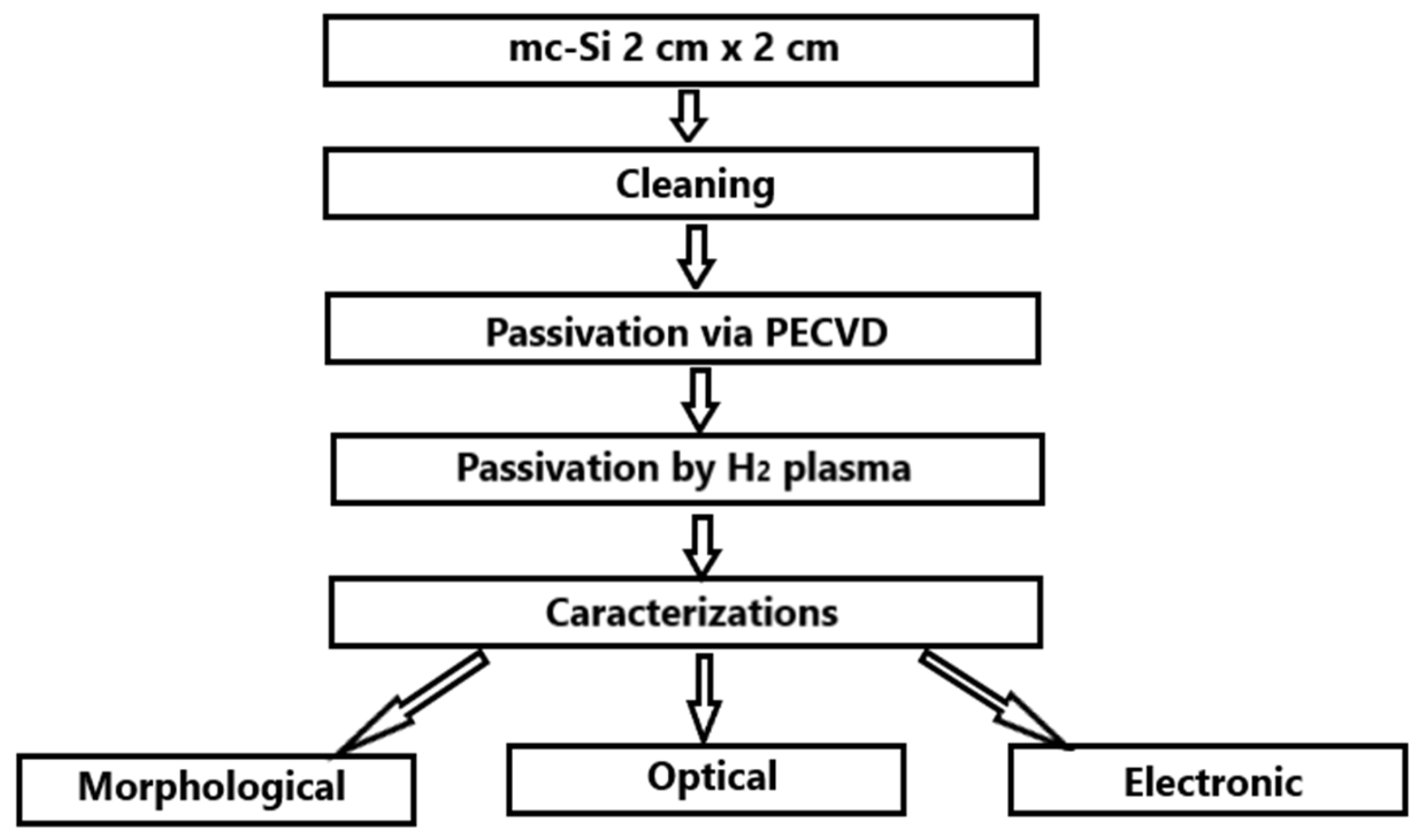
The experimental protocol is illustrated in Figure 8. This study was designed to evaluate the effect of hydrogen plasma (H2) passivation treatment on p-type multicrystalline silicon (mc-Si) substrates with a resistivity of 0.5–2 Ω·cm, dimensions of 2 × 2 cm2, and a thickness of 400 µm. First, the samples underwent cleaning using a 10 wt.% hydrofluoric acid solution prepared by diluting commercial HF (48 wt.%) to remove the native oxide layer and surface impurities that could negatively affect optical and electronic performance. After cleaning, the samples were rinsed with deionized water and dried under a nitrogen flux. Following this step, a hydrogen plasma (H2) passivation treatment is applied using plasma-enhanced chemical vapor deposition. The samples treated are then subjected to a series of characterizations to assess their properties, including morphological characterizations, optical analyses and electronic measurements. This structured protocol allows for an effective evaluation of the studied passivation.

3.1. Silicon Properties

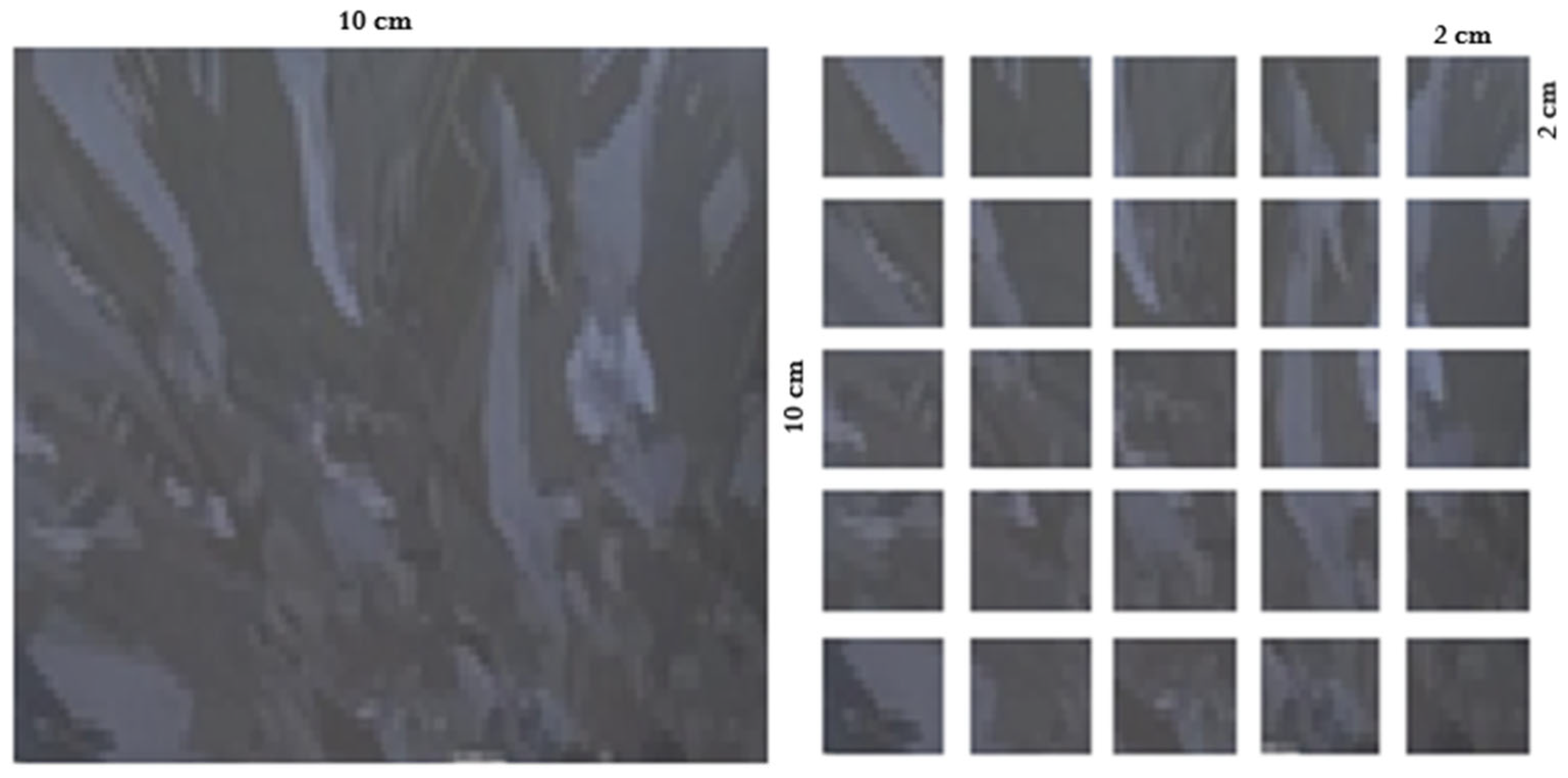
The multicrystalline silicon (mc-Si) used in this work was produced via directional solidification, a process that is faster and less expensive than monocrystalline growth but generally yields lower efficiencies due to variable crystal sizes, dislocations, and impurities. For this study, p-type mc-Si wafers with a thickness of 400 µm and a resistivity of 0.5–2.0 Ω·cm were diced from the original 10 × 10 cm2 wafers into smaller 2 × 2 cm2 pieces using a diamond scribe (Figure 9). These samples were subsequently employed for hydrogen plasma treatment and further characterization. The main physical properties of the mc-Si wafers are summarized in Table 4.

3.2. Cleaning Process

Silicon’s highly reactive nature and strong affinity for atmospheric oxygen make it difficult to prepare and maintain an atomically clean surface. Consequently, an effective pre-deposition cleaning procedure is essential for achieving stable, reproducible, and high-quality surface passivation. This step plays a decisive role in determining the efficiency of subsequent chemical passivation processes. A widely adopted approach in the microelectronics and photovoltaics industries involves the use of a diluted hydrofluoric acid solution. The primary objective of this treatment is the dissolution and removal of the native silicon oxide layer (typically a few nanometers thick) that naturally forms on the surface of silicon wafers. After deoxidation, the wafers are rinsed thoroughly with deionized water and then dried using a stream of high-purity nitrogen gas.

3.3. Hydrogen Plasma Deposition

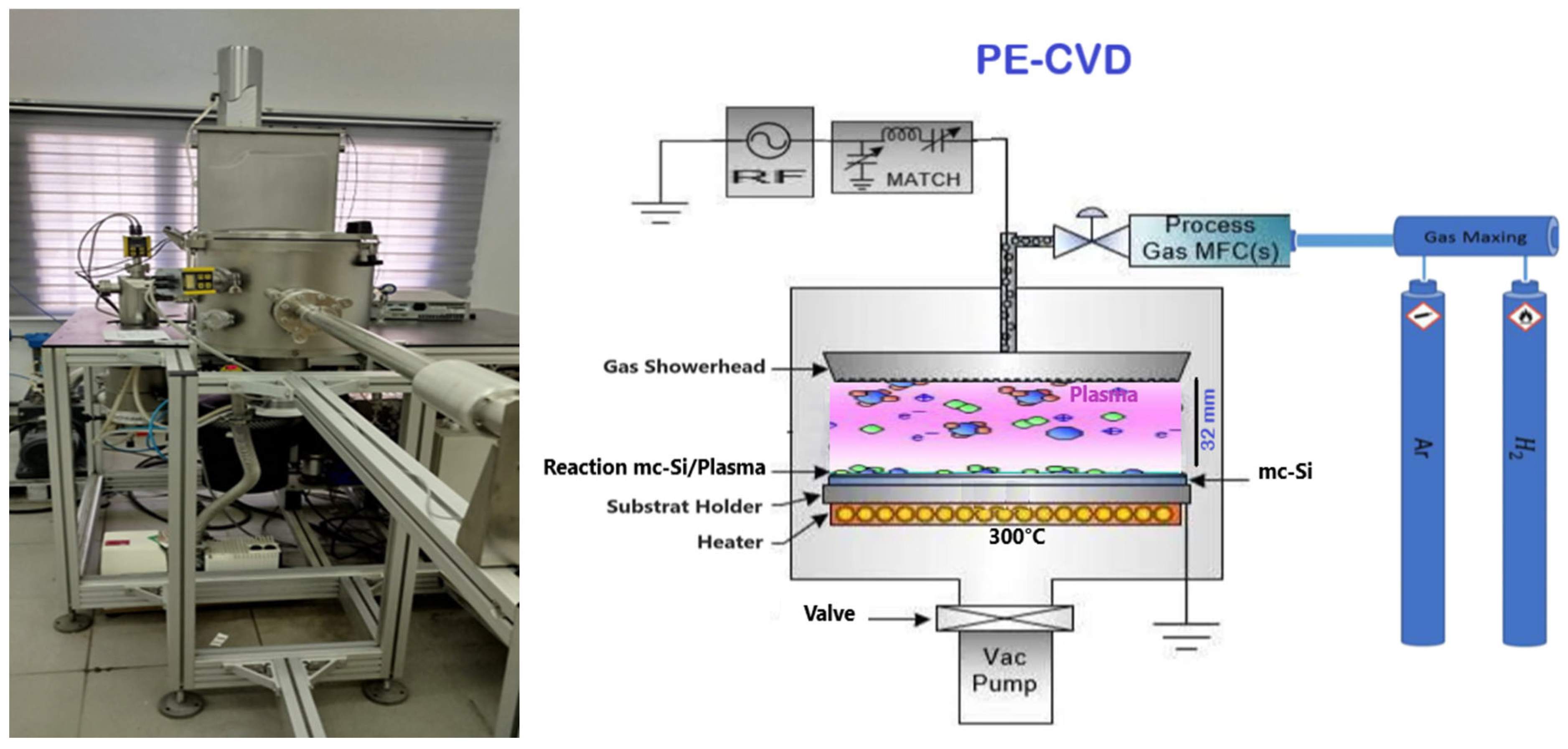
After the cleaning process, hydrogen plasma treatment was applied via the PE-CVD reactor [28] to passivate the surface and bulk of the mc-silicon. The PE-CVD reactor (Elettrorava S.p.A., Venaria Reale, Italy), as shown in Figure 10, is equipped with a reaction chamber that is separated from a load-lock chamber by a vacuum valve and maintained under high vacuum (≤10−6 mbar) using turbo-molecular and rotary vane pumps. The process is controlled by a PLC and uses a 13.56 MHz RF generator to generate the plasma. The substrate is placed on a graphite electrode with a temperature range of 50 °C to 500 °C. Importantly, the hydrogen radicals generated in the plasma chemically passivate dangling bonds, suppressing electronic defects and improving electrical performance. During PE-CVD processing at 300–450 °C, hydrogen penetration in crystalline silicon is generally reported to be relatively shallow. Several experimental and diffusion studies indicate that the penetration depth is typically in the sub-micron to ~1–2 µm range, depending on the plasma power, exposure time, and microstructure of the material [36,43]. Hydrogen plasma treatment was performed in a PE-CVD system under controlled conditions. Cleaned mc-Si substrates were placed in a vacuum chamber (base pressure ~10−5–10−6 Torr) and heated to 300 °C. After introducing high-purity H2 gas, the pressure stabilized at 100 mTorr, and an RF power of 60 W (13.56 MHz) was applied to generate plasma. The samples were exposed for 5 min. During this period, reactive hydrogen species penetrated the near-surface region of silicon and passivated dangling bonds and defect sites, particularly at grain boundaries. No film deposition occurred; the treatment resulted solely in hydrogen incorporation and defect passivation. The optimized operating parameters are listed in Table 5.

4. Conclusions

This study highlights the significant impact of hydrogen plasma treatment on the properties of multicrystalline silicon (mc-Si). PE-CVD-based hydrogen treatment enhances the structural, optical, electrical, and electronic characteristics of mc-Si wafers, lowering surface reflectivity from 26% to 15%, increasing diffusion length from 56 µm to 100 µm (≈79% improvement), and extending carrier lifetime from 1 µs to 3 µs (200% increase). Dark I–V analysis shows a 32% reduction in series resistance, a 51% increase in shunt resistance, and a 28% reduction in dark saturation current, reflecting improved carrier transport, suppressed leakage, and enhanced solar cell efficiency. LBIC mapping indicates a 14% rise in the grain boundary current, demonstrating the effective passivation of defect-rich regions and reduced recombination. In the main, H2 plasma PE-CVD treatment proves to be an effective strategy for improving the optoelectronic quality and photovoltaic performance of mc-Si wafers. The quantitative improvements in minority carrier lifetime, diffusion length, and dark saturation current clearly demonstrate the effectiveness of hydrogen plasma passivation in enhancing the electrical and electronic quality of high-efficiency solar cells, making mc-Si wafers more suitable for advanced photovoltaic and semiconductor applications.

Author Contributions

Conceptualization, A.E.H., H.N. and M.B.R.; methodology, A.E.H. and A.M.; software, K.C.; validation, W.D., K.C. and M.A.A.; formal analysis, M.A.A.; investigation, A.E.H. and H.N.; resources, M.B.R.; data curation, A.M. and M.A.A.; writing—original draft preparation, M.B.R. and A.E.H.; writing—review and editing, K.C. and M.B.R.; visualization, W.D.; supervision, M.B.R.; project administration, K.C.; funding acquisition, K.C. All authors have read and agreed to the published version of the manuscript.

Funding

This work was supported and funded by the Deanship of Scientific Research at Imam Mohammad Ibn Saud Islamic University (IMSIU) (grant number IMSIU-DDRSP2602).

Institutional Review Board Statement

Not applicable.

Informed Consent Statement

Not applicable.

Data Availability Statement

The datasets generated and/or analyzed during the current study are available from the corresponding author upon reasonable request.

Conflicts of Interest

The authors declare no conflicts of interest.

References

  1. Izam, N.S.M.N.; Itam, Z.; Sing, W.L.; Syamsir, A. Sustainable Development Perspectives of Solar Energy Technologies with Focus on Solar Photovoltaic—A Review. Energies 2022, 15, 2790. [Google Scholar] [CrossRef]
  2. Wang, A.; Lin, Q.; Liu, C.; Yang, L.; Sun, S. Sustainable Energy Development: Reviewing Carbon Emission Reduction in Photovoltaic Power Systems. Sustainability 2024, 16, 10428. [Google Scholar] [CrossRef]
  3. Liu, D.; Liu, J.; Wang, S.; Xu, M.; Akbar, S.J. Contribution of international photovoltaic trade to global greenhouse gas emission reduction: The example of China. Resour. Conserv. Recycl. 2019, 143, 114–118. [Google Scholar] [CrossRef]
  4. Ben Rabha, M.; El Haj, A.; Mannai, A.; Choubani, K.; Almeshaal, M.A.; Dimassi, W. Enhancement of Optoelectronic Properties of Multicrystalline Silicon Using Al-NPs and SiNx Layer. Crystals 2025, 15, 381. [Google Scholar] [CrossRef]
  5. Burtescu, S.; Parvulescu, C.; Babarada, F.; Manea, E. The low cost multicrystalline silicon solar cells. Mater. Sci. Eng. B 2009, 165, 190–193. [Google Scholar] [CrossRef]
  6. Schindler, F.; Michl, B.; Krenckel, P.; Riepe, S.; Benick, J.; Müller, R.; Schubert, M.C. Optimized multicrystalline silicon for solar cells enabling conversion efficiencies of 22%. Sol. Energy Mater. Sol. Cells 2017, 171, 180–186. [Google Scholar] [CrossRef]
  7. Schindler, F.; Fell, A.; Müller, R.; Benick, J.; Richter, A.; Feldmann, F.; Glunz, S.W. Towards the efficiency limits of multicrystalline silicon solar cells. Sol. Energy Mater. Sol. Cells 2018, 185, 198–204. [Google Scholar] [CrossRef]
  8. Möller, H.J.; Funke, C.; Rinio, M.; Scholz, S. Multicrystalline silicon for solar cells. Thin Solid Film. 2005, 487, 179–187. [Google Scholar] [CrossRef]
  9. Gurusamy, A.; Manickam, S.; Perumalsamy, R. Quality improvement of multi-crystalline silicon ingot by the Hot-Zone modification. J. Cryst. Growth 2022, 592, 126720. [Google Scholar] [CrossRef]
  10. Suchikova, Y.; Nazarovets, S.; Konuhova, M.; Popov, A.I. Binary Oxide Ceramics (TiO2, ZnO, Al2O3, SiO2, CeO2, Fe2O3, and WO3) for Solar Cell Applications: A Comparative and Bibliometric Analysis. Ceramics 2025, 8, 4. [Google Scholar] [CrossRef]
  11. Iturralde Carrera, L.A.; Garcia-Barajas, M.G.; Constantino-Robles, C.D.; Álva-rez-Alvarado, J.M.; Castillo-Alvarez, Y.; Rodríguez-Reséndiz, J. Efficiency and Sustainability in Solar Photovoltaic Systems: A Review of Key Factors and Innovative Technologies. Eng 2025, 6, 50. [Google Scholar] [CrossRef]
  12. Yu, W.; Xue, Y.; Mei, J.; Zhou, X.; Xiong, M.; Zhang, S. Segregation and removal of transition metal impurities during the directional solidification refining of silicon with Al-Si solvent. J. Alloys Compd. 2019, 805, 198–204. [Google Scholar] [CrossRef]
  13. Lv, X.; Li, H.; Ding, D.; Yu, X.; Jin, C.; Yang, D. Interfacial characterization of non-metal precipitates at grain boundaries in cast multicrystalline silicon crystals. J. Cryst. Growth 2025, 652, 128042. [Google Scholar] [CrossRef]
  14. Wang, L.; Liu, J.; Li, Y.; Wei, G.; Li, Q.; Fan, Z.; He, D. Dislocations in Crystalline Silicon Solar Cells. Adv. Energy Sustain. Res. 2024, 5, 2300240. [Google Scholar] [CrossRef]
  15. Chen, J.; Chen, B.; Lee, W.; Fukuzawa, M.; Yamada, M.; Sekiguchi, T. Grain boundaries in multicrystalline Si. Solid State Phenom. 2010, 156, 19–26. [Google Scholar] [CrossRef]
  16. Woo, S.; Bertoni, M.; Choi, K.; Nam, S.; Castellanos, S.; Powell, D.M.; Choi, H. An insight into dislocation density reduction in multicrystalline silicon. Sol. Energy Mater. Sol. Cells 2016, 155, 88–100. [Google Scholar] [CrossRef]
  17. Hu, D.; Zhang, J.; Yuan, S.; Chen, H.; Wang, C.; Yu, X.; Cheng, X. Effects of metal impurities at the edges of cast Si ingot on crystal quality and solar cell performance. Sol. Energy 2022, 246, 224–233. [Google Scholar] [CrossRef]
  18. Hu, Z.; Lin, D.; Yu, X.; Seiffert, C.; Kuznetsov, A.; Yang, D. Role of metal impurities in multicrystalline silicon solar cell degradation. Appl. Phys. Express 2021, 14, 115502. [Google Scholar] [CrossRef]
  19. Ogundipe, O.B.; Okwandu, A.C.; Abdulwaheed, S.A. Recent advances in solar photovoltaic technologies: Efficiency, materials, and applications. GSC Adv. Res. Rev. 2024, 20, 159–175. [Google Scholar] [CrossRef]
  20. Dasilva-Villanueva, N.; Catalán-Gómez, S.; Marrón, D.F.; Torres, J.J.; García-Corpas, M.; del Cañizo, C. Reduction of trapping and recombination in upgraded metallurgical grade silicon: Impact of phosphorous diffusion gettering. Sol. Energy Mater. Sol. Cells 2022, 234, 111410. [Google Scholar] [CrossRef]
  21. Achref, M.; Bessadok, A.J.; Khezami, L.; Mokraoui, S.; Benrabha, M. Effective surface passivation on multi-crystalline silicon using aluminum/porous silicon nanostructures. Surf. Interfaces 2020, 18, 100391. [Google Scholar] [CrossRef]
  22. Alrasheedi, N.H. The effects of porous silicon and silicon nitride treatments on the electronic qualities of multicrystalline silicon for solar cell applications. Silicon 2024, 16, 1765–1773. [Google Scholar] [CrossRef]
  23. Almeshaal, M.A.; Abdouli, B.; Choubani, K.; Khezami, L.; Rabha, M.B. Study of porous silicon layer effect in optoelectronics properties of multi-crystalline silicon for photovoltaic applications. Silicon 2023, 15, 6025–6032. [Google Scholar] [CrossRef]
  24. Khezami, L.; Jemai, A.B.; Alhathlool, R.; Rabha, M.B. Electronic quality improvement of crystalline silicon by stain etching-based PS nanostructures for solar cells application. Sol. Energy 2016, 129, 38–44. [Google Scholar] [CrossRef]
  25. Porre, O.; Martinuzzi, S.; Pasquinelli, M.; Perichaud, I.; Gay, N. Gettering effect of aluminium in mc-Si and c-Si wafers and in solar cells. In Proceedings of the Conference Record of the Twenty Fifth IEEE Photovoltaic Specialists Conference, Washington, DC, USA, 13–17 May 1996; IEEE: Piscataway, NJ, USA, 1996. [Google Scholar]
  26. Liu, A.; Sun, C.; Sio, H.C.; Zhang, X.; Jin, H.; Macdonald, D. Gettering of Transition Metals in High-Performance Multicrystalline Silicon by Silicon Nitride Films and Phosphorus Diffusion. J. Appl. Phys. 2019, 125, 043103. [Google Scholar] [CrossRef]
  27. Sun, C.; Liu, A.; Samadi, A.; Chan, C.; Ciesla, A.; Macdonald, D. Transition Metals in a Cast-Monocrystalline Silicon Ingot Studied by Silicon Nitride Gettering. Phys. Status Solidi RRL 2019, 13, 1900456. [Google Scholar] [CrossRef]
  28. Mannai, A.; Benabderrahmane Zaghouani, R.; Choubani, K.; Almeshaal, M.A.; Rabha, M.B.; Dimassi, W. Electronic Quality Enhancement of Multicrystalline Silicon via SiNx and H2 Plasma Passivation Using Plasma-Enhanced Chemical Vapor Deposition for Photovoltaic Applications. Crystals 2025, 15, 498. [Google Scholar] [CrossRef]
  29. Pandey, A.; Bhattacharya, S.; Alam, S.; Manna, S.; Sadhukhan, S.; Singh, S.P.; Komarala, V.K. Influence of Very High-Frequency PECVD Hydrogen Plasma Treatment on Intrinsic Amorphous Silicon Passivation Stack: Impact on Silicon Heterojunction Solar Cell Performance. ACS Appl. Energy Mater. 2025, 8, 366–375. [Google Scholar] [CrossRef]
  30. Li, Z.; Yang, Z.; Wang, J.; Liu, A.; Murad, A.; Sun, C.; Han, W.; Wang, Y.; Nguyen, H.; Macdonald, D. Effective hydrogen diffusivity in n-and p-type crystalline silicon from 300 to 450° C. J. Appl. Phys. 2026, 139, 035702. [Google Scholar] [CrossRef]
  31. Dominguez, M.; Rosales, P.; Torres, A. Performance improvement of low-temperature a-SiGe: H thin-film transistors. Solid-State Electron. 2012, 76, 44–47. [Google Scholar] [CrossRef]
  32. Moreno, M.; Torres-Sánchez, A.; Rosales, P.; Morales, A.; Torres, A.; Flores, J.; Hernández, L.; Zúñiga, C.; Ascencio, C.; Arenas, A. Effect of the RF Power of PECVD on the Crystalline Fractions of Microcrystalline Silicon (μc-Si:H) Films and Their Structural, Optical, and Electronic Properties. Electron. Mater. 2023, 4, 110–123. [Google Scholar] [CrossRef]
  33. Choubani, K.; Zouari, Y.; El Haj, A.; Mannai, A.; Almeshaal, M.A.; Dimassi, W.; Ben Rabha, M. Enhancing Optoelectronic Properties of Multicrystalline Silicon Using Dual Treatments for Solar Cell Applications. Inorganics 2025, 13, 142. [Google Scholar] [CrossRef]
  34. Barrio, R.; González, N.; Cárabe, J.; Gandía, J.J. Optimisation of NaOH texturisation process of silicon wafers for heterojunction solar-cells applications. Sol. Energy 2012, 86, 845–854. [Google Scholar] [CrossRef]
  35. Goldie, D.M.; Persheyev, S.K. Quantitative hydrogen measurements in PECVD and HWCVD a-Si:H using FTIR spectroscopy. J. Mater. Sci. 2006, 41, 5287–5291. [Google Scholar] [CrossRef]
  36. Van de Walle, C.G.; Neugebauer, J. Hydrogen in semiconductors. Annu. Rev. Mater. Res. 2006, 36, 179–198. [Google Scholar] [CrossRef]
  37. Han, D.; Wang, K.; Owens, J.M.; Gedvilas, L.; Nelson, B.; Habuchi, H.; Tanaka, M. Hydrogen structures and the optoelectronic properties in transition films from amorphous to microcrystalline silicon prepared by hot-wire chemical vapor deposition. J. Appl. Phys. 2003, 93, 3776–3783. [Google Scholar] [CrossRef]
  38. Shinohara, M.; Kuwano, T.; Akama, Y.; Kimura, Y.; Niwano, M.; Ishida, H.; Hatakeyama, R. Interaction of hydrogen-terminated Si(100), (110), and (111) surfaces with hydrogen plasma investigated by in situreal-time infrared absorption spectroscopy. J. Vac. Sci. Technol. A 2003, 21, 25. [Google Scholar] [CrossRef]
  39. Wang, J.; Ru, X.; Ruan, T.; Hu, Y.; Zhang, Y.; Yan, H. Performance of heterojunction solar cells with different intrinsic a-Si: H thin layers deposited by RF-and VHF-PECVD. J. Mater. Sci. Mater. Electron. 2021, 32, 25327–25331. [Google Scholar] [CrossRef]
  40. Rabha, M.B.; Bessaïs, B. Enhancement of photovoltaic properties of multicrystalline silicon solar cells by combination of buried metallic contacts and thin porous silicon. Sol. Energy 2010, 84, 486–491. [Google Scholar] [CrossRef]
  41. Nouri, H.; Choubani, K.; Ouertani, R.; Ben Rabha, M. Investigation of the Electrical Mechanism in an Ag/pSiO2/Si MIS Heterojunction: Effect of the Oxidation Temperature. Crystals 2025, 15, 763. [Google Scholar] [CrossRef]
  42. Tsurekawa, S.; Kido, K.; Hamada, S.; Watanabe, T.; Sekiguchi, T. Electrical activity of grain boundaries in polycrystalline silicon influences grain boundary structure, chemistry and temperature. Int. J. Mater. Res. 2005, 96, 197–206. [Google Scholar] [CrossRef]
  43. Seager, C.H.; Ginley, D.S. Studies of the hydrogen passivation of silicon grain boundaries. J. Appl. Phys. 1981, 52, 1050–1055. [Google Scholar] [CrossRef]
Figure 1. Surface morphology of multicrystalline silicon before and after PE-CVD treatment measured by profilometry.
Inorganics 14 00105 g001aInorganics 14 00105 g001b
Figure 2. Reflectivity spectrum of mc-Si substrate before and after PE-CVD treatment.
Inorganics 14 00105 g002
Figure 3. FT-IR spectra of multicrystalline silicon after H2 plasma PE-CVD treatment; the untreated mc-Si sample was used as background reference during FT-IR measurements.
Inorganics 14 00105 g003
Figure 4. Mapping of the effective lifetime and corresponding histograms of the wafers: (a) reference, (b) after PE-CVD hydrogen plasma.
Inorganics 14 00105 g004aInorganics 14 00105 g004b
Figure 5. Mapping of the effective diffusion length and corresponding histograms of the wafers: (a) reference, (b) after PE-CVD hydrogen plasma.
Inorganics 14 00105 g005
Figure 6. Dark I–V characteristic of the mc-Si solar cell before and after treatment.
Inorganics 14 00105 g006
Figure 7. Normalized LBIC profiles measured on mc-Si solar cells around the same GBs before and after treatment.
Inorganics 14 00105 g007
Figure 8. Experimental process.
Inorganics 14 00105 g008
Figure 9. Multicrystalline silicon wafer before and after cut.
Inorganics 14 00105 g009
Figure 10. Plasma-enhanced chemical vapor deposition reactor.
Inorganics 14 00105 g010
Table 1. Root-mean-square (RMS) roughness values before and after treatment.
Sample ConditionSurface RoughnessObservation
Reference0.37 μmBaseline roughness of the untreated material.
Treated mc-Si0.51 μmThe PE-CVD treatment results in a significant increase in surface irregularities. This surface texturing is optically beneficial, as it enhances light trapping and scattering in photovoltaic devices.
Table 2. Electrical parameters extracted from the dark I–V.
Bare mc-SiTreated mc-SiImprovement
Rs (Ω)191332%
Rsh (Ω)16625051%
Table 3. Effect of H2 Plasma Treatment on the Optical and Electrical Properties of mc-Si Wafers.
SampleReflectivity (%)Diffusion Length (µm)Lifetime (µs)Rs (Ω)Rsh (Ω)LBIC
Ref mc-Si26561191660.73
Treated mc-Si151003132500.83
Improvement42%79%200%32%51%14%
Table 4. The mc-silicon wafer’s properties.
MaterialsMulticrystalline Silicon (mc-Si), p-Type
Produced via Directional Solidification
Wafer thickness400 µm
Active area(2 cm × 2 cm)
Resistivity0.5–2.0 Ω·cm
Table 5. Optimized PE-CVD parameters for hydrogen plasma treatment.
ParametersValue
Deposition Time5 min
Deposition Temperature300 °C
Deposition Pressure100 mTorr
RF Power60 W
Radio Frequency13.6 Hz
Disclaimer/Publisher’s Note: The statements, opinions and data contained in all publications are solely those of the individual author(s) and contributor(s) and not of MDPI and/or the editor(s). MDPI and/or the editor(s) disclaim responsibility for any injury to people or property resulting from any ideas, methods, instructions or products referred to in the content.