
Electrical and Electronic Quality Improvement of Multicrystalline Silicon Solar Cells via Hydrogen Plasma Treatment

 , and
, and 
Abstract
1. Introduction
2. Results and Discussions
3. Experimental Procedure
3.1. Silicon Properties
3.2. Cleaning Process
3.3. Hydrogen Plasma Deposition
4. Conclusions
Author Contributions
Funding
Institutional Review Board Statement
Informed Consent Statement
Data Availability Statement
Conflicts of Interest
References
- Izam, N.S.M.N.; Itam, Z.; Sing, W.L.; Syamsir, A. Sustainable Development Perspectives of Solar Energy Technologies with Focus on Solar Photovoltaic—A Review. Energies 2022, 15, 2790. [Google Scholar] [CrossRef]
- Wang, A.; Lin, Q.; Liu, C.; Yang, L.; Sun, S. Sustainable Energy Development: Reviewing Carbon Emission Reduction in Photovoltaic Power Systems. Sustainability 2024, 16, 10428. [Google Scholar] [CrossRef]
- Liu, D.; Liu, J.; Wang, S.; Xu, M.; Akbar, S.J. Contribution of international photovoltaic trade to global greenhouse gas emission reduction: The example of China. Resour. Conserv. Recycl. 2019, 143, 114–118. [Google Scholar] [CrossRef]
- Ben Rabha, M.; El Haj, A.; Mannai, A.; Choubani, K.; Almeshaal, M.A.; Dimassi, W. Enhancement of Optoelectronic Properties of Multicrystalline Silicon Using Al-NPs and SiNx Layer. Crystals 2025, 15, 381. [Google Scholar] [CrossRef]
- Burtescu, S.; Parvulescu, C.; Babarada, F.; Manea, E. The low cost multicrystalline silicon solar cells. Mater. Sci. Eng. B 2009, 165, 190–193. [Google Scholar] [CrossRef]
- Schindler, F.; Michl, B.; Krenckel, P.; Riepe, S.; Benick, J.; Müller, R.; Schubert, M.C. Optimized multicrystalline silicon for solar cells enabling conversion efficiencies of 22%. Sol. Energy Mater. Sol. Cells 2017, 171, 180–186. [Google Scholar] [CrossRef]
- Schindler, F.; Fell, A.; Müller, R.; Benick, J.; Richter, A.; Feldmann, F.; Glunz, S.W. Towards the efficiency limits of multicrystalline silicon solar cells. Sol. Energy Mater. Sol. Cells 2018, 185, 198–204. [Google Scholar] [CrossRef]
- Möller, H.J.; Funke, C.; Rinio, M.; Scholz, S. Multicrystalline silicon for solar cells. Thin Solid Film. 2005, 487, 179–187. [Google Scholar] [CrossRef]
- Gurusamy, A.; Manickam, S.; Perumalsamy, R. Quality improvement of multi-crystalline silicon ingot by the Hot-Zone modification. J. Cryst. Growth 2022, 592, 126720. [Google Scholar] [CrossRef]
- Suchikova, Y.; Nazarovets, S.; Konuhova, M.; Popov, A.I. Binary Oxide Ceramics (TiO2, ZnO, Al2O3, SiO2, CeO2, Fe2O3, and WO3) for Solar Cell Applications: A Comparative and Bibliometric Analysis. Ceramics 2025, 8, 4. [Google Scholar] [CrossRef]
- Iturralde Carrera, L.A.; Garcia-Barajas, M.G.; Constantino-Robles, C.D.; Álva-rez-Alvarado, J.M.; Castillo-Alvarez, Y.; Rodríguez-Reséndiz, J. Efficiency and Sustainability in Solar Photovoltaic Systems: A Review of Key Factors and Innovative Technologies. Eng 2025, 6, 50. [Google Scholar] [CrossRef]
- Yu, W.; Xue, Y.; Mei, J.; Zhou, X.; Xiong, M.; Zhang, S. Segregation and removal of transition metal impurities during the directional solidification refining of silicon with Al-Si solvent. J. Alloys Compd. 2019, 805, 198–204. [Google Scholar] [CrossRef]
- Lv, X.; Li, H.; Ding, D.; Yu, X.; Jin, C.; Yang, D. Interfacial characterization of non-metal precipitates at grain boundaries in cast multicrystalline silicon crystals. J. Cryst. Growth 2025, 652, 128042. [Google Scholar] [CrossRef]
- Wang, L.; Liu, J.; Li, Y.; Wei, G.; Li, Q.; Fan, Z.; He, D. Dislocations in Crystalline Silicon Solar Cells. Adv. Energy Sustain. Res. 2024, 5, 2300240. [Google Scholar] [CrossRef]
- Chen, J.; Chen, B.; Lee, W.; Fukuzawa, M.; Yamada, M.; Sekiguchi, T. Grain boundaries in multicrystalline Si. Solid State Phenom. 2010, 156, 19–26. [Google Scholar] [CrossRef]
- Woo, S.; Bertoni, M.; Choi, K.; Nam, S.; Castellanos, S.; Powell, D.M.; Choi, H. An insight into dislocation density reduction in multicrystalline silicon. Sol. Energy Mater. Sol. Cells 2016, 155, 88–100. [Google Scholar] [CrossRef]
- Hu, D.; Zhang, J.; Yuan, S.; Chen, H.; Wang, C.; Yu, X.; Cheng, X. Effects of metal impurities at the edges of cast Si ingot on crystal quality and solar cell performance. Sol. Energy 2022, 246, 224–233. [Google Scholar] [CrossRef]
- Hu, Z.; Lin, D.; Yu, X.; Seiffert, C.; Kuznetsov, A.; Yang, D. Role of metal impurities in multicrystalline silicon solar cell degradation. Appl. Phys. Express 2021, 14, 115502. [Google Scholar] [CrossRef]
- Ogundipe, O.B.; Okwandu, A.C.; Abdulwaheed, S.A. Recent advances in solar photovoltaic technologies: Efficiency, materials, and applications. GSC Adv. Res. Rev. 2024, 20, 159–175. [Google Scholar] [CrossRef]
- Dasilva-Villanueva, N.; Catalán-Gómez, S.; Marrón, D.F.; Torres, J.J.; García-Corpas, M.; del Cañizo, C. Reduction of trapping and recombination in upgraded metallurgical grade silicon: Impact of phosphorous diffusion gettering. Sol. Energy Mater. Sol. Cells 2022, 234, 111410. [Google Scholar] [CrossRef]
- Achref, M.; Bessadok, A.J.; Khezami, L.; Mokraoui, S.; Benrabha, M. Effective surface passivation on multi-crystalline silicon using aluminum/porous silicon nanostructures. Surf. Interfaces 2020, 18, 100391. [Google Scholar] [CrossRef]
- Alrasheedi, N.H. The effects of porous silicon and silicon nitride treatments on the electronic qualities of multicrystalline silicon for solar cell applications. Silicon 2024, 16, 1765–1773. [Google Scholar] [CrossRef]
- Almeshaal, M.A.; Abdouli, B.; Choubani, K.; Khezami, L.; Rabha, M.B. Study of porous silicon layer effect in optoelectronics properties of multi-crystalline silicon for photovoltaic applications. Silicon 2023, 15, 6025–6032. [Google Scholar] [CrossRef]
- Khezami, L.; Jemai, A.B.; Alhathlool, R.; Rabha, M.B. Electronic quality improvement of crystalline silicon by stain etching-based PS nanostructures for solar cells application. Sol. Energy 2016, 129, 38–44. [Google Scholar] [CrossRef]
- Porre, O.; Martinuzzi, S.; Pasquinelli, M.; Perichaud, I.; Gay, N. Gettering effect of aluminium in mc-Si and c-Si wafers and in solar cells. In Proceedings of the Conference Record of the Twenty Fifth IEEE Photovoltaic Specialists Conference, Washington, DC, USA, 13–17 May 1996; IEEE: Piscataway, NJ, USA, 1996. [Google Scholar]
- Liu, A.; Sun, C.; Sio, H.C.; Zhang, X.; Jin, H.; Macdonald, D. Gettering of Transition Metals in High-Performance Multicrystalline Silicon by Silicon Nitride Films and Phosphorus Diffusion. J. Appl. Phys. 2019, 125, 043103. [Google Scholar] [CrossRef]
- Sun, C.; Liu, A.; Samadi, A.; Chan, C.; Ciesla, A.; Macdonald, D. Transition Metals in a Cast-Monocrystalline Silicon Ingot Studied by Silicon Nitride Gettering. Phys. Status Solidi RRL 2019, 13, 1900456. [Google Scholar] [CrossRef]
- Mannai, A.; Benabderrahmane Zaghouani, R.; Choubani, K.; Almeshaal, M.A.; Rabha, M.B.; Dimassi, W. Electronic Quality Enhancement of Multicrystalline Silicon via SiNx and H2 Plasma Passivation Using Plasma-Enhanced Chemical Vapor Deposition for Photovoltaic Applications. Crystals 2025, 15, 498. [Google Scholar] [CrossRef]
- Pandey, A.; Bhattacharya, S.; Alam, S.; Manna, S.; Sadhukhan, S.; Singh, S.P.; Komarala, V.K. Influence of Very High-Frequency PECVD Hydrogen Plasma Treatment on Intrinsic Amorphous Silicon Passivation Stack: Impact on Silicon Heterojunction Solar Cell Performance. ACS Appl. Energy Mater. 2025, 8, 366–375. [Google Scholar] [CrossRef]
- Li, Z.; Yang, Z.; Wang, J.; Liu, A.; Murad, A.; Sun, C.; Han, W.; Wang, Y.; Nguyen, H.; Macdonald, D. Effective hydrogen diffusivity in n-and p-type crystalline silicon from 300 to 450° C. J. Appl. Phys. 2026, 139, 035702. [Google Scholar] [CrossRef]
- Dominguez, M.; Rosales, P.; Torres, A. Performance improvement of low-temperature a-SiGe: H thin-film transistors. Solid-State Electron. 2012, 76, 44–47. [Google Scholar] [CrossRef]
- Moreno, M.; Torres-Sánchez, A.; Rosales, P.; Morales, A.; Torres, A.; Flores, J.; Hernández, L.; Zúñiga, C.; Ascencio, C.; Arenas, A. Effect of the RF Power of PECVD on the Crystalline Fractions of Microcrystalline Silicon (μc-Si:H) Films and Their Structural, Optical, and Electronic Properties. Electron. Mater. 2023, 4, 110–123. [Google Scholar] [CrossRef]
- Choubani, K.; Zouari, Y.; El Haj, A.; Mannai, A.; Almeshaal, M.A.; Dimassi, W.; Ben Rabha, M. Enhancing Optoelectronic Properties of Multicrystalline Silicon Using Dual Treatments for Solar Cell Applications. Inorganics 2025, 13, 142. [Google Scholar] [CrossRef]
- Barrio, R.; González, N.; Cárabe, J.; Gandía, J.J. Optimisation of NaOH texturisation process of silicon wafers for heterojunction solar-cells applications. Sol. Energy 2012, 86, 845–854. [Google Scholar] [CrossRef]
- Goldie, D.M.; Persheyev, S.K. Quantitative hydrogen measurements in PECVD and HWCVD a-Si:H using FTIR spectroscopy. J. Mater. Sci. 2006, 41, 5287–5291. [Google Scholar] [CrossRef]
- Van de Walle, C.G.; Neugebauer, J. Hydrogen in semiconductors. Annu. Rev. Mater. Res. 2006, 36, 179–198. [Google Scholar] [CrossRef]
- Han, D.; Wang, K.; Owens, J.M.; Gedvilas, L.; Nelson, B.; Habuchi, H.; Tanaka, M. Hydrogen structures and the optoelectronic properties in transition films from amorphous to microcrystalline silicon prepared by hot-wire chemical vapor deposition. J. Appl. Phys. 2003, 93, 3776–3783. [Google Scholar] [CrossRef]
- Shinohara, M.; Kuwano, T.; Akama, Y.; Kimura, Y.; Niwano, M.; Ishida, H.; Hatakeyama, R. Interaction of hydrogen-terminated Si(100), (110), and (111) surfaces with hydrogen plasma investigated by in situreal-time infrared absorption spectroscopy. J. Vac. Sci. Technol. A 2003, 21, 25. [Google Scholar] [CrossRef]
- Wang, J.; Ru, X.; Ruan, T.; Hu, Y.; Zhang, Y.; Yan, H. Performance of heterojunction solar cells with different intrinsic a-Si: H thin layers deposited by RF-and VHF-PECVD. J. Mater. Sci. Mater. Electron. 2021, 32, 25327–25331. [Google Scholar] [CrossRef]
- Rabha, M.B.; Bessaïs, B. Enhancement of photovoltaic properties of multicrystalline silicon solar cells by combination of buried metallic contacts and thin porous silicon. Sol. Energy 2010, 84, 486–491. [Google Scholar] [CrossRef]
- Nouri, H.; Choubani, K.; Ouertani, R.; Ben Rabha, M. Investigation of the Electrical Mechanism in an Ag/pSiO2/Si MIS Heterojunction: Effect of the Oxidation Temperature. Crystals 2025, 15, 763. [Google Scholar] [CrossRef]
- Tsurekawa, S.; Kido, K.; Hamada, S.; Watanabe, T.; Sekiguchi, T. Electrical activity of grain boundaries in polycrystalline silicon influences grain boundary structure, chemistry and temperature. Int. J. Mater. Res. 2005, 96, 197–206. [Google Scholar] [CrossRef]
- Seager, C.H.; Ginley, D.S. Studies of the hydrogen passivation of silicon grain boundaries. J. Appl. Phys. 1981, 52, 1050–1055. [Google Scholar] [CrossRef]



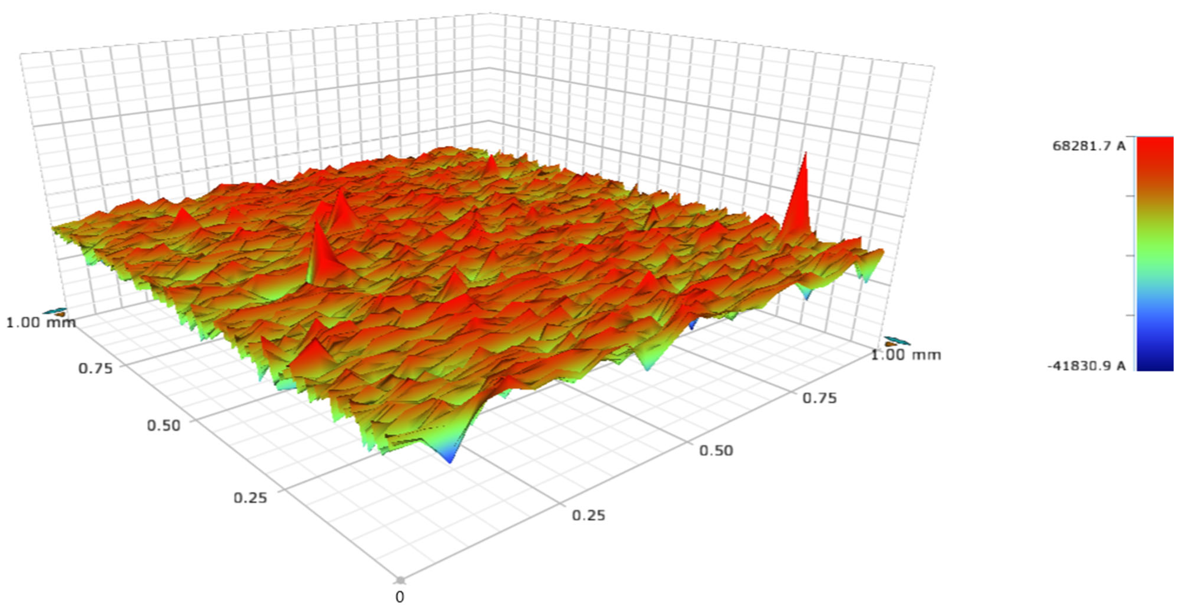
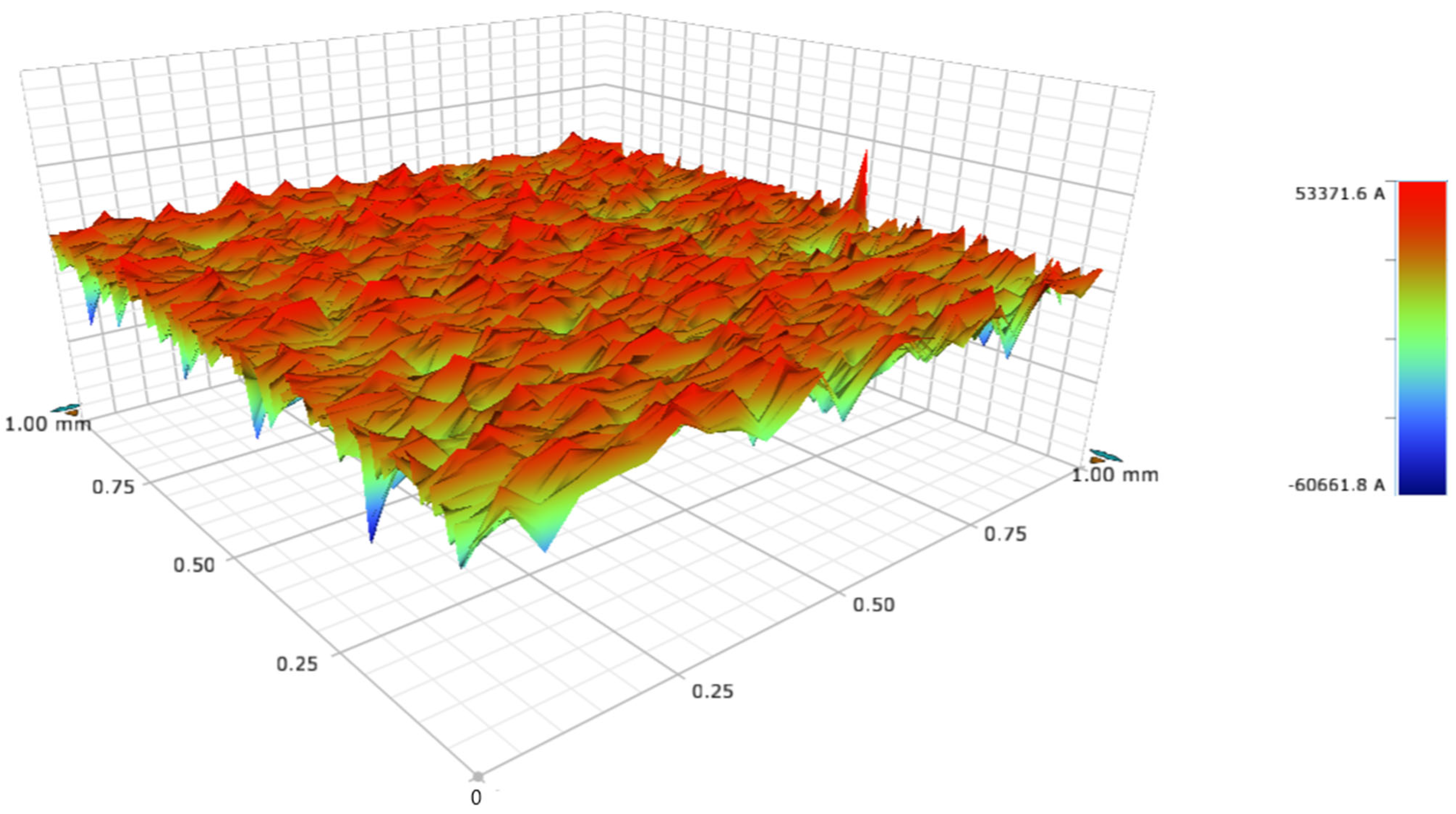
| Sample Condition | Surface Roughness | Observation |
|---|---|---|
| Reference | 0.37 μm | Baseline roughness of the untreated material. |
| Treated mc-Si | 0.51 μm | The PE-CVD treatment results in a significant increase in surface irregularities. This surface texturing is optically beneficial, as it enhances light trapping and scattering in photovoltaic devices. |
| Bare mc-Si | Treated mc-Si | Improvement | |
|---|---|---|---|
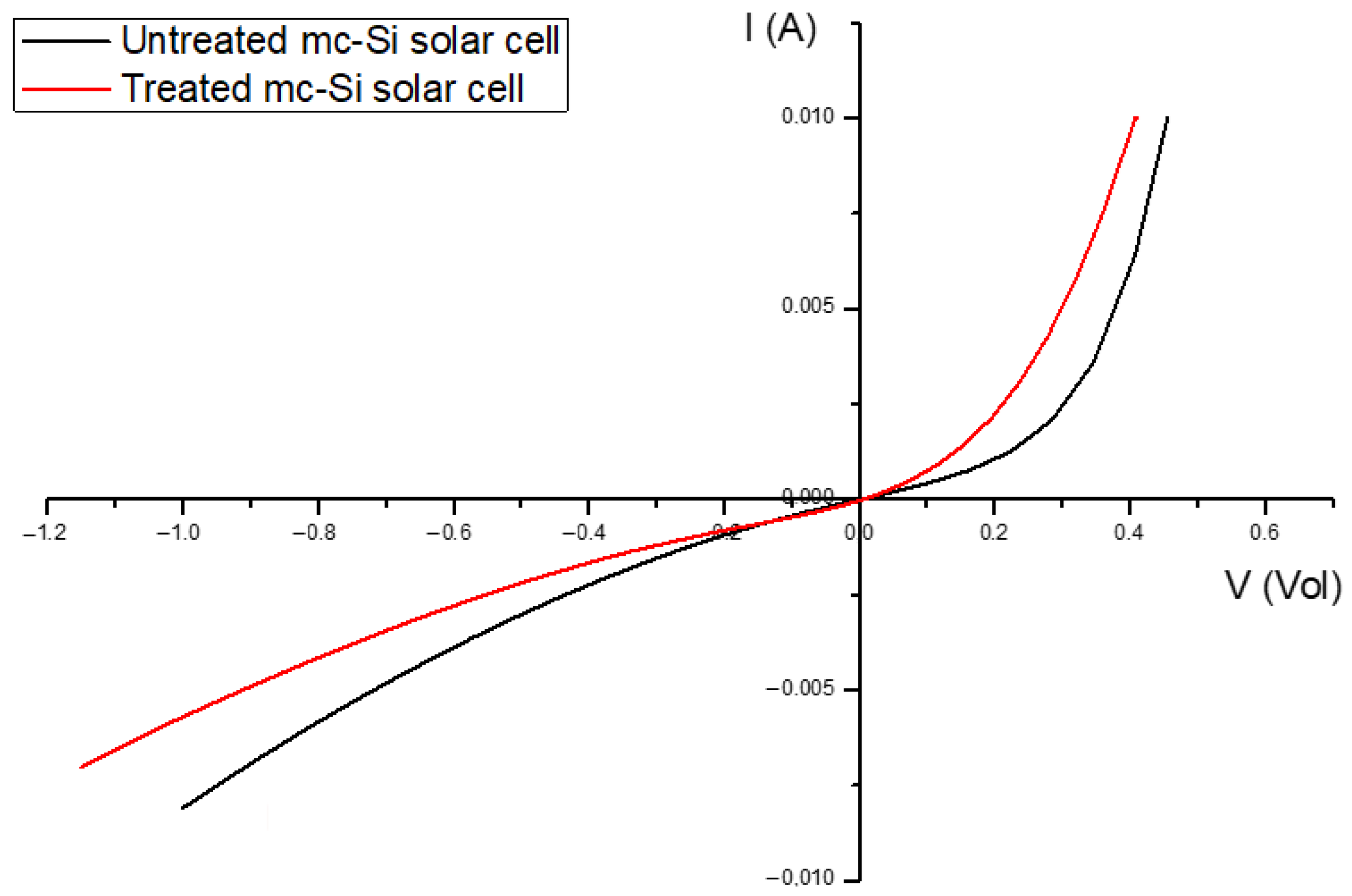
| Rs (Ω) | 19 | 13 | 32% |
| Rsh (Ω) | 166 | 250 | 51% |
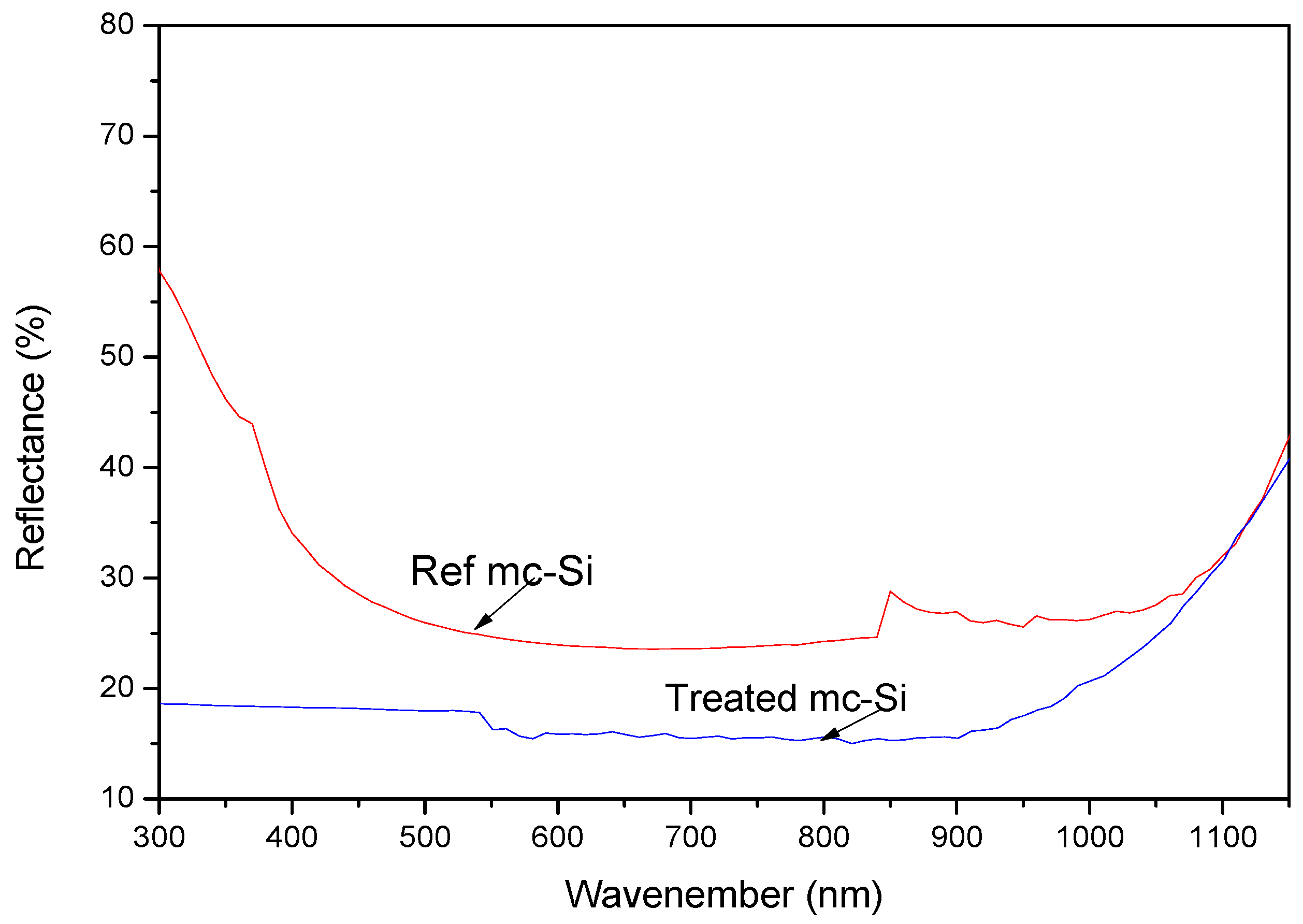
| Sample | Reflectivity (%) | Diffusion Length (µm) | Lifetime (µs) | Rs (Ω) | Rsh (Ω) | LBIC |
|---|---|---|---|---|---|---|
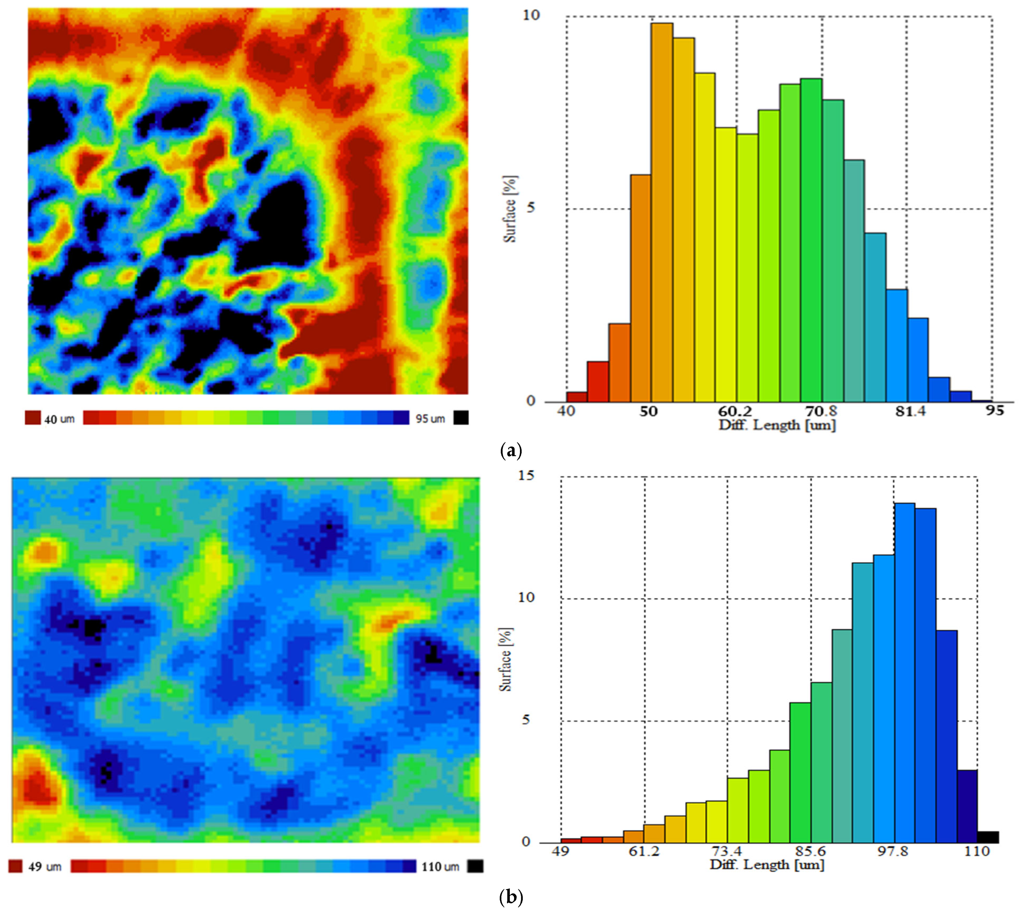
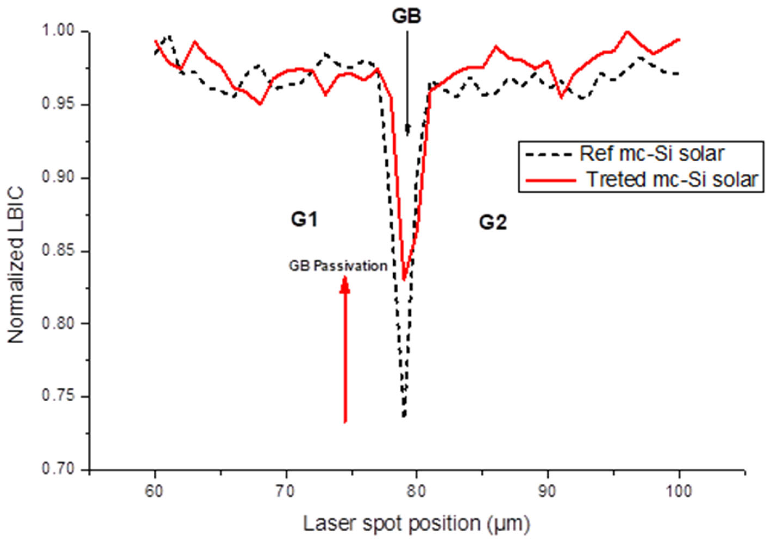
| Ref mc-Si | 26 | 56 | 1 | 19 | 166 | 0.73 |
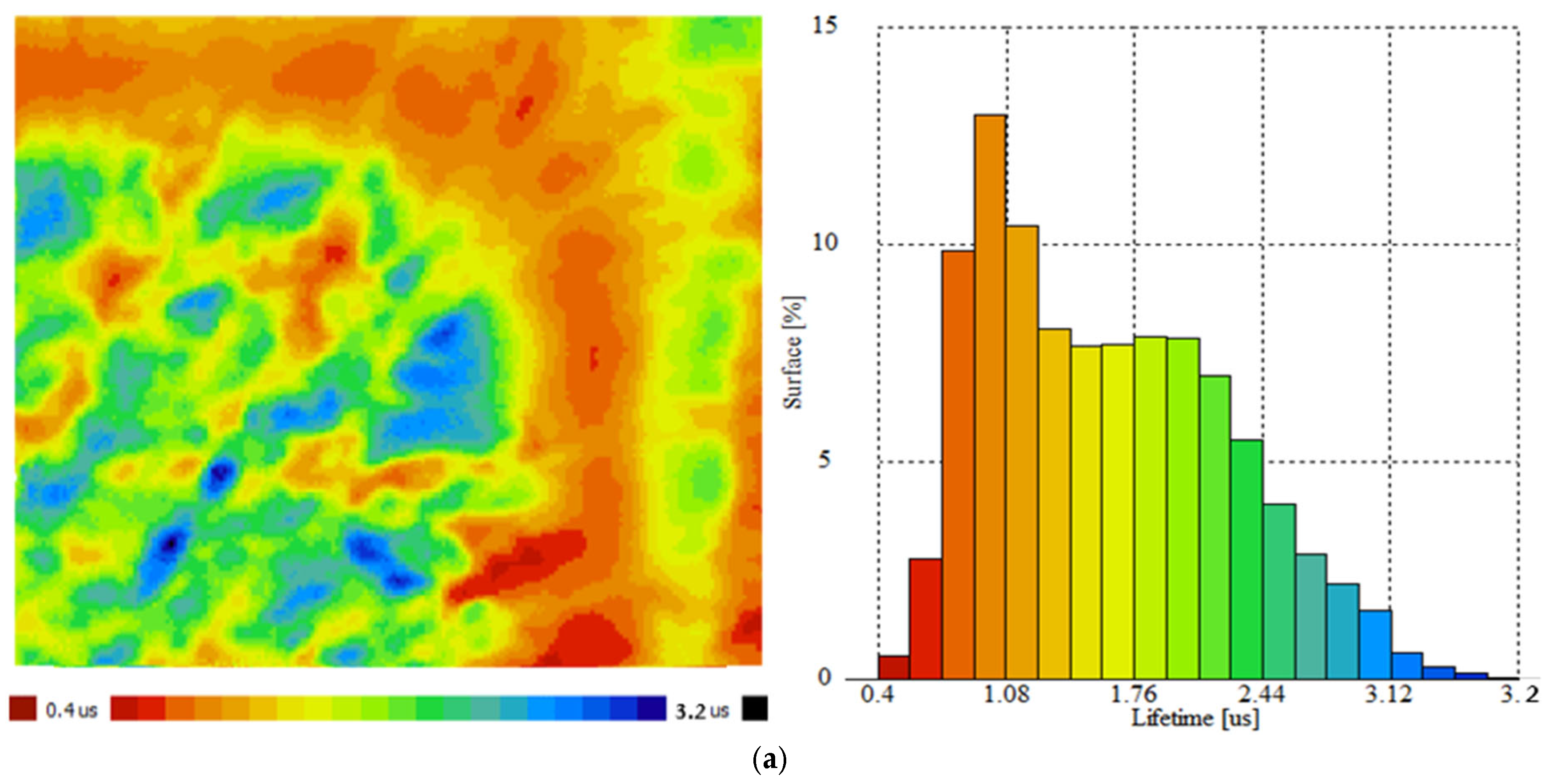
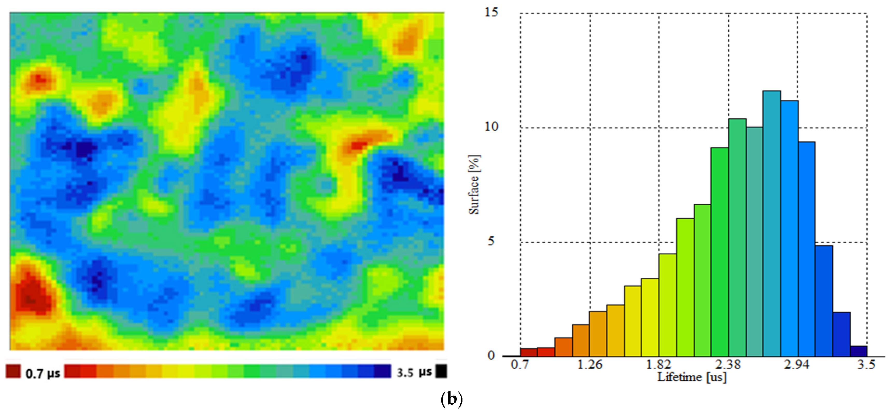
| Treated mc-Si | 15 | 100 | 3 | 13 | 250 | 0.83 |
| Improvement | 42% | 79% | 200% | 32% | 51% | 14% |
| Materials | Multicrystalline Silicon (mc-Si), p-Type Produced via Directional Solidification |
|---|---|
| Wafer thickness | 400 µm |
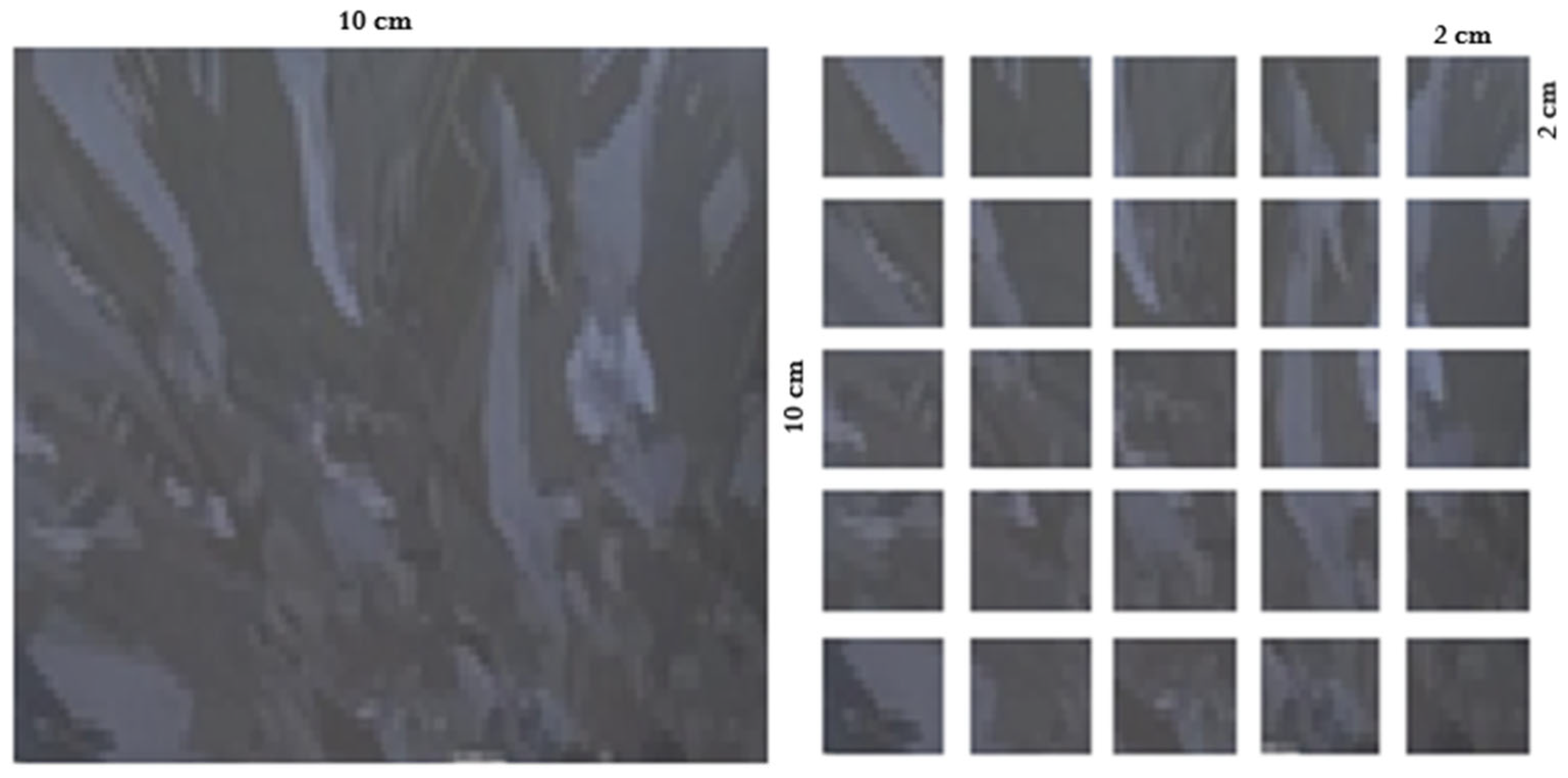
| Active area | (2 cm × 2 cm) |
| Resistivity | 0.5–2.0 Ω·cm |
| Parameters | Value |
|---|---|
| Deposition Time | 5 min |
| Deposition Temperature | 300 °C |
| Deposition Pressure | 100 mTorr |
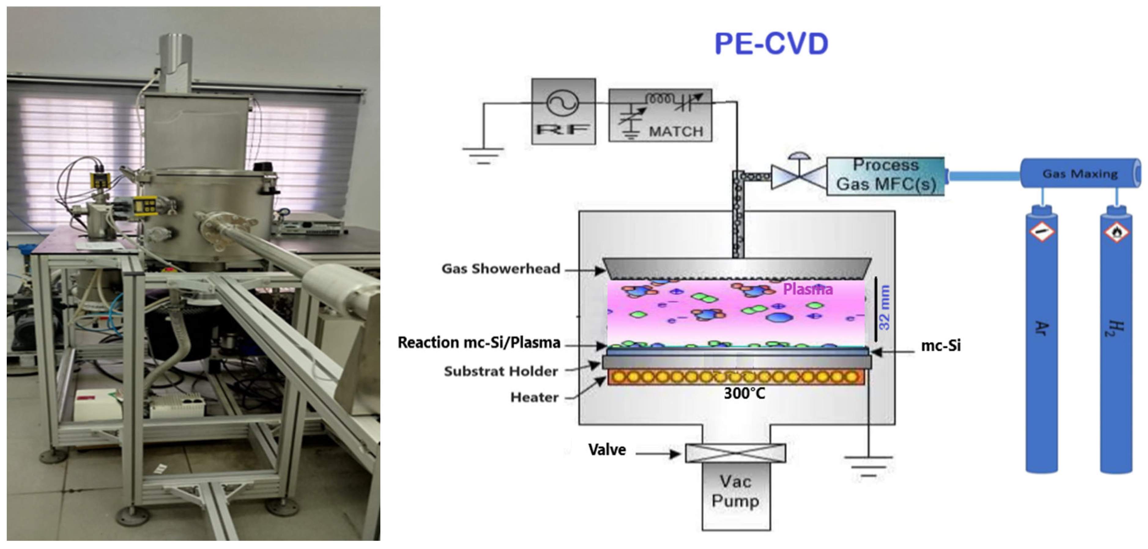
| RF Power | 60 W |
| Radio Frequency | 13.6 Hz |
Disclaimer/Publisher’s Note: The statements, opinions and data contained in all publications are solely those of the individual author(s) and contributor(s) and not of MDPI and/or the editor(s). MDPI and/or the editor(s) disclaim responsibility for any injury to people or property resulting from any ideas, methods, instructions or products referred to in the content. |
© 2026 by the authors. Licensee MDPI, Basel, Switzerland. This article is an open access article distributed under the terms and conditions of the Creative Commons Attribution (CC BY) license.
Share and Cite
El Haj, A.; Mannai, A.; Nouri, H.; Choubani, K.; Almeshaal, M.A.; Dimassi, W.; Rabha, M.B. Electrical and Electronic Quality Improvement of Multicrystalline Silicon Solar Cells via Hydrogen Plasma Treatment. Inorganics 2026, 14, 105. https://doi.org/10.3390/inorganics14040105
El Haj A, Mannai A, Nouri H, Choubani K, Almeshaal MA, Dimassi W, Rabha MB. Electrical and Electronic Quality Improvement of Multicrystalline Silicon Solar Cells via Hydrogen Plasma Treatment. Inorganics. 2026; 14(4):105. https://doi.org/10.3390/inorganics14040105
Chicago/Turabian StyleEl Haj, Ameny, Achref Mannai, Hassen Nouri, Karim Choubani, Mohammed A. Almeshaal, Wissem Dimassi, and Mohamed Ben Rabha. 2026. "Electrical and Electronic Quality Improvement of Multicrystalline Silicon Solar Cells via Hydrogen Plasma Treatment" Inorganics 14, no. 4: 105. https://doi.org/10.3390/inorganics14040105
APA StyleEl Haj, A., Mannai, A., Nouri, H., Choubani, K., Almeshaal, M. A., Dimassi, W., & Rabha, M. B. (2026). Electrical and Electronic Quality Improvement of Multicrystalline Silicon Solar Cells via Hydrogen Plasma Treatment. Inorganics, 14(4), 105. https://doi.org/10.3390/inorganics14040105