1. Introduction
Graphitic carbon nitride (g-C
3N
4) has attracted considerable attention due to its visible-light absorption, favorable electrical properties, excellent band structure, and high physicochemical stability. It features a layered structure analogous to graphene, consisting of π-conjugated graphitic sheets formed by alternating sp
2-hybridized carbon and nitrogen atoms. Adjacent layers are bound by weak van der Waals forces, whereas strong in-plane covalent bonds hold atoms together within each individual layer, ensuring structural stability [
1]. The primary building block of g-C
3N
4 is the tri-s-triazine (C
6N
7) unit, interconnected through planar tertiary nitrogen atoms. As a rising polymeric semiconductor, g-C
3N
4 exhibits a suitable bandgap of approximately 2.7 eV. Bulk g-C
3N
4 demonstrates promising applicability in solar energy conversion and visible-light harvesting [
2]. Compared to bulk g-C
3N
4, low-dimensional nanostructures have gained growing interest owing to their high surface-to-volume ratio, stronger absorption in the blue-light region, superior charge carrier separation, and enhanced electron transport capability. The energy bandgap of 2D g-C
3N
4 nanostructures increases compared to the bulk material, primarily due to quantum confinement effects arising from reduced dimensionality [
3]. The optoelectronic properties of 2D g-C
3N
4 can be tuned by controlling the degree of polymerization, defect density, heteroatom types, and functional groups through synthetic conditions, precursor selection, and post-synthetic functionalization [
4]. Moreover, g-C
3N
4 boasts further benefits such as negligible toxicity, high natural abundance, and low cost. As a metal-free semiconductor, it has become a compelling candidate for sustainable technologies, particularly in environmental remediation, energy-efficient systems, and green applications. To date, 2D g-C
3N
4 nanostructures have been widely explored in CO
2 reduction, pollutant degradation, water splitting, and photocatalysis owing to their excellent photochemical properties [
5,
6,
7]. Furthermore, advances in understanding their photophysical properties have enabled novel applications in areas such as sensors, imaging, solar cells, smart responsive systems, and memory devices [
8,
9,
10,
11].
Photodetectors are optoelectronic devices that convert optical signals into electrical signals. With the rapid advancement of modern technologies, they have become increasingly important in aerospace, defense, and industry, finding applications in remote sensing, night vision, space communications, security screening, missile guidance, environmental monitoring, and biomedical imaging [
12,
13,
14]. To comprehensively evaluate photodetector performance, several key figures of merit are commonly employed. Responsivity quantifies the electrical output per unit of optical input power, with higher values indicating greater sensitivity. Specific detectivity represents the ability to detect weak signals, normalized for noise and area; a higher specific detectivity is crucial for low-light applications. The response speed, characterized by rise/fall times, determines the device’s capability for high-frequency operation. For self-powered photodetectors, a significant photocurrent under zero bias is an additional critical metric, demonstrating energy-efficient operation. Owing to its outstanding optoelectronic performance, natural abundance, cost-effective preparation, and robust stability, two-dimensional g-C
3N
4 is considered a highly viable candidate for photodetection applications. In recent years, photodetectors based on g-C
3N
4 have attracted growing interest and have achieved significant progress in performance and functionality [
15]. For instance, Shan et al. developed a flexible 2D g-C
3N
4 photodetector array exhibiting a fast response time (6/8 ms), high on/off ratio (~250), broadband UV sensitivity, and outstanding mechanical stability, successfully demonstrating its capability in a 10 × 10 UV imaging system [
16]. Shan and Dong et al. also demonstrated that high pressure enhances g-C
3N
4 photodetection, doubling responsivity and photocurrent at 3.6 GPa due to bandgap reduction from increased interlayer interaction [
17]. Heterojunction structures are fundamentally preferred in photodiode and photovoltaic device design due to their ability to create a built-in electric field at the interface. This field enables highly efficient separation of photogenerated electron-hole pairs and suppresses their recombination, leading to superior quantum efficiency and responsivity [
18,
19]. Furthermore, heterostructures allow for bandgap engineering, facilitating broadband light absorption and tailored spectral response, which are critical for high-performance optoelectronics [
20]. To enhance photodetection performance and improve exciton dissociation efficiency, researchers have developed various g-C
3N
4-based heterostructures to boost their photoresponse. Notable examples include 2D/2D g-C
3N
4 nanosheets/graphene, 2D/2D MoS
2/g-C
3N
4, 1D/2D g-C
3N
4/CNTs, 0D/2D g-C
3N
4/Bi
2S
3, 0D/2D g-C
3N
4/CdS, 0D/2D hybrid-dimensional g-C
3N
4/Bi, and 0D/1D g-C
3N
4 QDs/ZnO nanowire heterostructures, each leveraging interfacial engineering to promote charge separation and extend spectral response [
21,
22,
23,
24,
25,
26,
27]. Alshareef et al. reported a flexible MoS
2/g-C
3N
4 photodetector on paper with broadband response (300–700 nm), high responsivity (4 A/W), detectivity (4 × 10
11 Jones), fast response (~50/80 ms), and excellent bending stability, supported by efficient charge transfer confirmed via femtosecond spectroscopy [
21]. Furthermore, a variety of g-C
3N
4-based 2D/3D heterojunction photodetectors have been explored and shown to be promising for self-powered, high-speed, and high-performance photodetection, owing to the built-in electric fields at the interface that enable efficient separation and rapid transport of photogenerated carriers [
2,
28,
29,
30,
31,
32]. Kim et al. developed vertical CN/Si photodiodes that function both as electrical diodes with exceptionally high rectification ratio (3.8 × 10
8) and photodetectors with high specific detectivity (1.9 × 10
12 Jones), wide linear operational range (>130 dB), and fast response (6.7 µs) [
33]. An isotype heterojunction is an interface between two different semiconductors with the same type of conductivity, such as an n-n junction. g-C3N4-based isotype heterojunction was also used as photodetectors. He and colleagues developed a sulfur-doped g-C
3N
4/GaN thin-film n-n heterojunction for blue-to-ultraviolet photodetection, demonstrating exceptional performance with a specific detectivity reaching 2.06 × 10
14 Jones and an extremely high on/off current ratio of 7.3 × 10
7 [
34].
Inspired by these studies, we have designed a self-powered, high-performance photodetector using a g-C3N4/textured Si n-n isotype heterojunction fabricated through a simple solution-based method. The device exhibits excellent diode characteristics with a rectification ratio of ~4.9 × 10² and an ideality factor of 1.41, indicating high junction quality. Benefiting from the synergistic effects of g-C3N4’s favorable optoelectronic characteristics and the superior light-trapping capability of textured Si, the photodetector achieves broadband response (405–980 nm), a high responsivity of 3.2 A/W, a specific detectivity of 1.9 × 10¹⁴ Jones, and fast response speeds of 44/36 ms at 650 nm under zero bias. Notably, the performance of the textured Si-based device is approximately tenfold higher than that of the planar Si counterpart due to significantly enhanced light absorption. The combination of outstanding photoresponse characteristics and straightforward fabrication promotes the g-C3N4/textured Si n-n heterojunction as a promising candidate for cost-effective, high-performance optoelectronic applications.
2. Results and Discussion
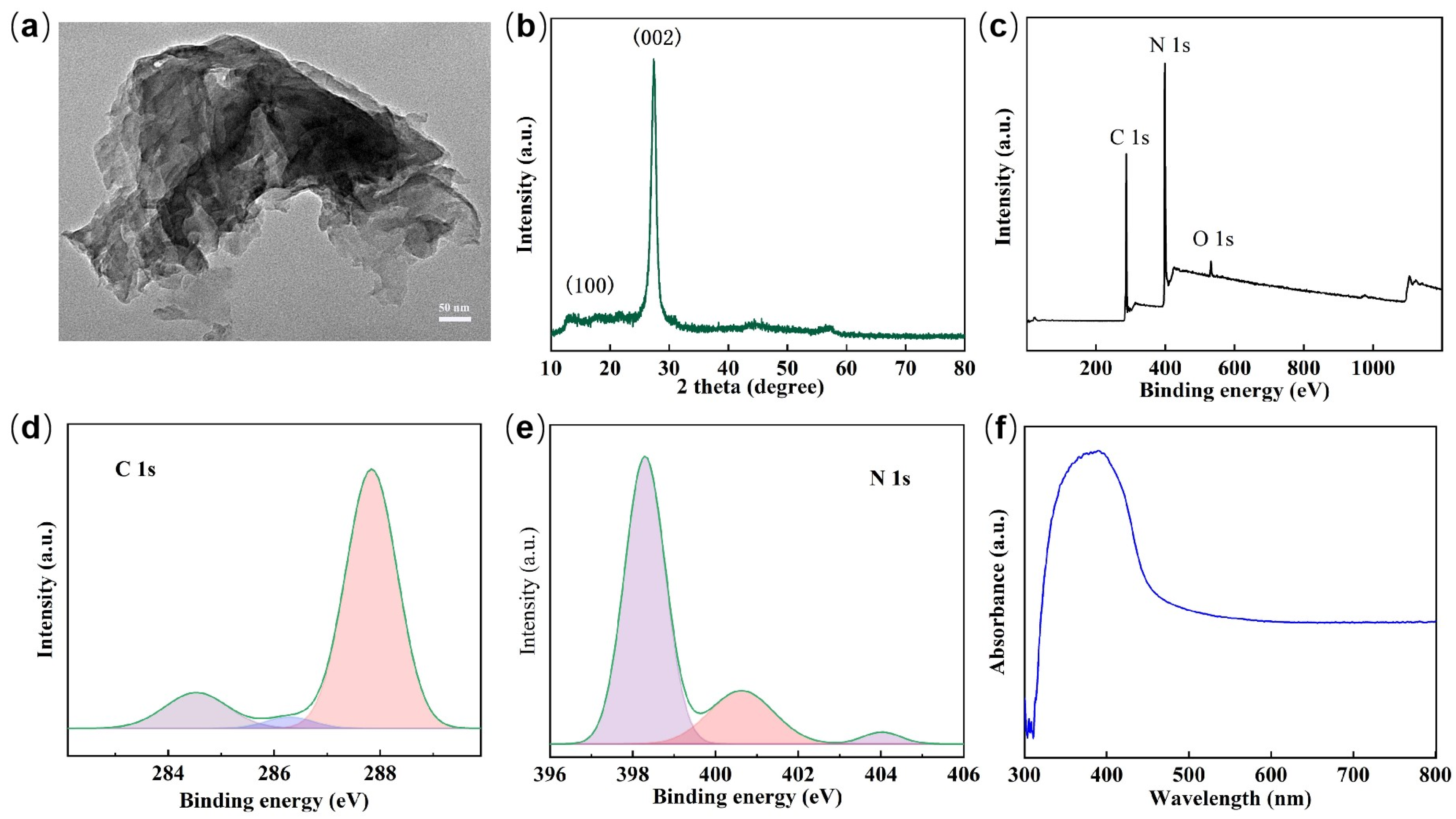
The TEM image of a representative g-C
3N
4 sample, shown in
Figure 1a, clearly reveals the preservation of a layered, lamellar morphology with lateral dimensions in the range of several hundred nanometers. The nanosheets exhibit smooth, flat surfaces and well-defined edges, indicating high structural integrity.
Figure 1b presents the XRD pattern of the as-prepared g-C
3N
4, displaying two distinct diffraction peaks at approximately 13.38° and 27.48°, both of which are sharp and well-resolved, confirming the crystalline nature of the material. It is widely recognized that g-C
3N
4 is composed of tri-s-triazine units. The peak at ~27.48° corresponds to the (002) plane and is attributed to the periodic interlayer stacking of conjugated aromatic layers, characteristic of graphitic structures. The lower-angle peak at 13.38° is assigned to the (001) plane, reflecting in-plane structural ordering and the distance between repeating triazine units along the c-axis [
35]. The elemental composition and chemical bonding states of g-C
3N
4 were systematically investigated using X-ray photoelectron spectroscopy. As shown in
Figure 1c, the XPS survey spectrum clearly reveals the presence of carbon (C 1s), nitrogen (N 1s), and a small amount of oxygen (O 1s), with the latter likely arising from surface adsorption of atmospheric species or minor oxidation. High-resolution analysis of the C 1s spectrum (
Figure 1d) reveals three distinct components after deconvolution. The peak at 284.5 eV is typically assigned to adventitious carbon contamination, such as graphitic C=C bonds from exposure to air. The component at 286.3 eV corresponds to carbon atoms in C=N or C≡N environments, possibly associated with structural defects or edge sites in sp
2-hybridized carbon networks. The dominant peak at 287.9 eV is attributed to sp
2-hybridized carbon in the N=C-N
2 configuration, characteristic of the heptazine (tri-s-triazine) units that form the backbone of g-C
3N
4. Similarly, the N 1s spectrum (
Figure 1e) is resolved into three peaks: 398.3 eV (sp
2-hybridized nitrogen in C-N=C, part of the triazine rings), 400.6 eV (tertiary nitrogen in N-(C)
3 groups, bridging nitrogen atoms), and 404.1 eV (π-excitations or amino groups, C-N-H, likely from terminal -NH or -NH
2 groups), confirming the expected chemical structure of polymeric carbon nitride [
27]. The UV-Vis absorption spectrum of g-C
3N
4, shown in
Figure 1f, reveals strong light absorption in the wavelength range of 320 to 450 nm, corresponding to the visible blue and near-UV region. The absorption edge is observed at approximately 450 nm, from which an optical bandgap of about 2.7 eV is estimated, consistent with the typical semiconductor characteristics of graphitic carbon nitride and indicating its suitability for visible and near-UV photodetection applications [
36].
To harness the optoelectronic potential of g-C
3N
4, we fabricated a g-C
3N
4/textured Si n-n heterojunction by a simple and scalable solution-based method, involving the drop-casting of a well-dispersed g-C
3N
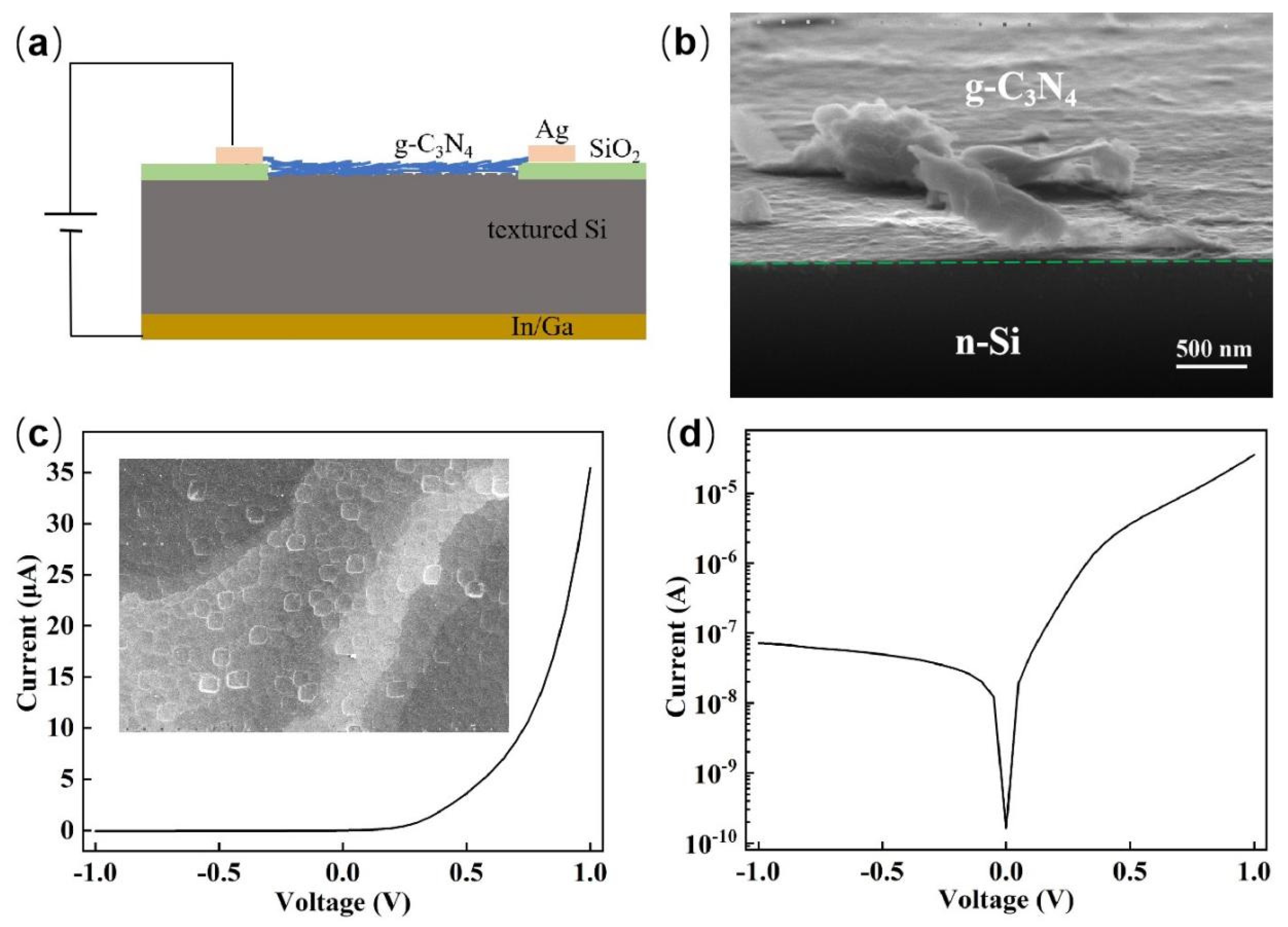
4 suspension onto a pre-patterned, textured silicon substrate.
Figure 2a illustrates a cross-sectional schematic of the resulting device, highlighting its vertically stacked architecture and external electrical connections. The structure consists sequentially of a silver (Ag) top electrode, the g-C
3N
4 layer, the textured n-type Si substrate, and an In/Ga eutectic alloy bottom electrode.
Figure 2b presents the corresponding cross-sectional scanning electron microscopy image, clearly distinguishing theg-C
3N
4 film from the underlying Si substrate. Notably, the g-C
3N
4 layer exhibits a thickness of several tens of nanometers and a complex, stratified morphology with folded nanosheets. The cross-sectional SEM image in
Figure 2b demonstrates excellent interfacial contact between the g-C
3N
4 layer and the textured Si substrate. This is verified by the observation of a continuous and conformal g-C
3N
4 film that closely follows the contours of the textured Si surface without visible cracks, gaps, or signs of peeling at the interface, which are typical indicators of poor adhesion or delamination. This intimate and continuous interface is highly beneficial for efficient charge carrier transport and collection across the heterojunction, laying a solid foundation for high-performance photodetection. On the other hand, in the top-view SEM image, the aggregated particles are identified as clusters of g-C
3N
4 nanosheets, which is a common morphology for materials derived from thermal condensation. While these aggregates create some surface roughness, the underlying film remains continuous and well adhered to the Si, as evidenced by the cross-sectional view. Therefore, these aggregates do not signify poor bulk adhesion but are a characteristic of the deposited film’s topography. Furthermore, the electrical characteristics of the g-C
3N
4/textured Si n-n heterojunction were evaluated by measuring the current–voltage (
I-V) curves under dark conditions at room temperature, as shown in
Figure 2c (linear scale) and
Figure 2d (semi-logarithmic scale). The device exhibits a clear current rectification behavior, with a rectification ratio of ~4.9 × 10
2 at ± 1V, indicating the formation of an effective junction barrier. This rectifying behavior primarily arises from the n-n heterojunction formed between the g-C
3N
4 and the n-type textured Si, where differences in electron affinity and work function create a built-in potential at the interface. The diode ideality factor (
n) was calculated to be around 1.41 by fitting the forward-bias
I-V data using the standard thermionic emission model:
, where
T is the absolute temperature,
kB is Boltzmann’s constant,
q is the elementary charge, respectively [
37]. Notably, the ideality factor close to 1.41 is significantly lower than those reported for many other g-C
3N
4-based heterojunctions and approaches the ideal value of 1, which corresponds to a diffusion-limited diode with minimal recombination [
28,
32]. Together, the high rectification ratio and low ideality factor strongly suggest excellent junction quality, efficient carrier transport, and low interface defect density in the fabricated device.
Furthermore, the barrier height (Φb) of the heterojunction was calculated based on the standard thermionic emission model. Using the saturation current (I0) extracted from the dark I-V characteristics, Φb was determined via the formula Φb = (kT/q) ln(AA*T2/I0), where A* is the effective Richardson constant, A is the contact area, k is Boltzmann’s constant, and T is the temperature. The calculated barrier height is approximately 0.81 eV. This value directly reflects the band alignment at the g-C3N4/textured Si interface. A moderate barrier height is crucial for efficiently separating photogenerated carriers under zero bias, forming the fundamental physical basis for the device’s self-powered operation. Moreover, this barrier height value corroborates the previously derived ideality factor (n ≈ 1.41), indicating the presence of certain recombination centers at the interface. This provides a key parameter for understanding the device’s performance variation under high light intensity.
The photodetection performance of the as-fabricated g-C
3N
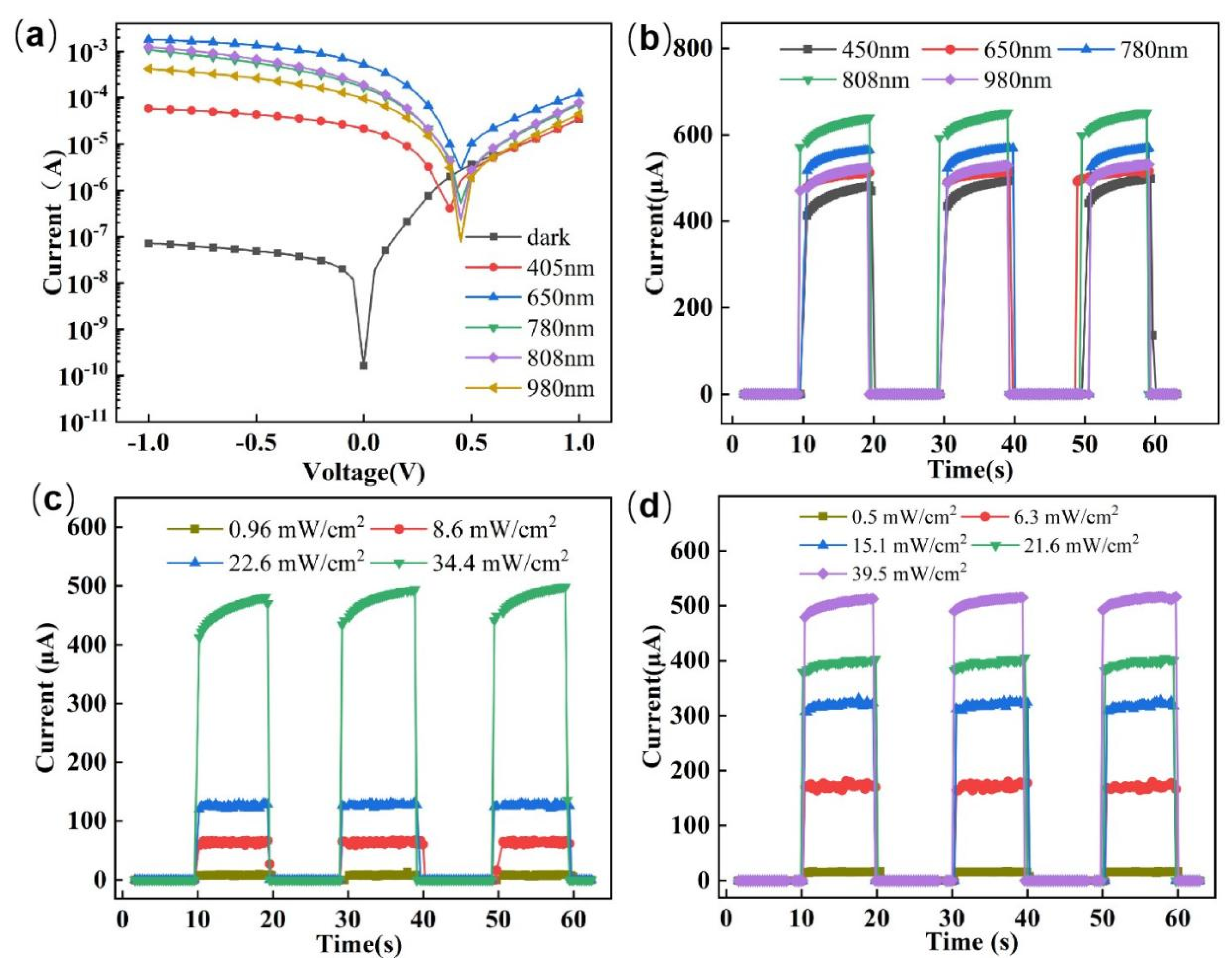
4/textured Si n-n heterojunction was thoroughly investigated under illumination with light sources of various wavelengths, including 405 nm, 650 nm, 780 nm, and 980 nm. As shown in
Figure 3,b, the device exhibits a significant increase in current under reverse bias upon light exposure, demonstrating its high sensitivity to incident photons. This response spans a broad spectral range from visible to near-infrared (NIR) light, confirming the device’s capability for broadband photodetection. Notably, the heterojunction also displays a strong photovoltaic effect, generating a measurable photocurrent and photovoltage in the absence of any external bias, as clearly illustrated in
Figure 3a. This enables the device to operate in a self-powered mode, which is highly desirable for low-energy-consumption and portable optoelectronic applications.
Figure 3b presents the time-resolved photovoltaic response of the device under periodic on/off illumination at different wavelengths without an external power supply. The current shows rapid, stable, and repeatable switching between dark and illuminated states, with sharp rising and falling edges across all tested wavelengths. This behavior reflects fast carrier generation, efficient charge separation at the heterojunction interface, and excellent response kinetics.
Figure 3c,d illustrate the time-dependent photoresponse of the g-C
3N
4/textured Si n-n heterojunction in self-powered mode under varying light intensities at wavelengths of 405 nm and 650 nm, respectively. The photocurrent increases progressively with higher incident light intensity, demonstrating the device’s excellent sensitivity and dynamic range. This trend directly translates into a significant enhancement in the light-to-dark current ratio (
Ilight/
Idark), which shows a clear positive correlation with increasing illumination intensity. Specifically, under 405 nm illumination, the
Ilight/
Idark ratio rises from approximately ~8.1 × 10
3 at a low intensity of 0.96 mW/cm
2 to a remarkable ~4.7 × 10
5 at 34.4 mW/cm
2 (
Figure 3c). Similarly, at 650 nm, the ratio increases from ~1.6 × 10
4 at 0.5 mW/cm
2 to ~5.3× 10
5 at 39.5 mW/cm
2 (
Figure 3d), indicating strong and tunable photoresponse across the visible spectrum. The device exhibits fast response dynamics with sharp rise and fall times, excellent signal stability, and high repeatability over multiple on-off cycles at all intensity levels. These characteristics collectively confirm that the fabricated heterojunction functions as a high-performance, self-powered photodetector with broadband sensitivity from visible to near-infrared light. Its superior sensitivity, wide dynamic range, and robust operation highlight its promising potential for applications in optical communication, night vision systems, environmental monitoring, and other low-power optoelectronic technologies.
The photodetection performance of the g-C
3N
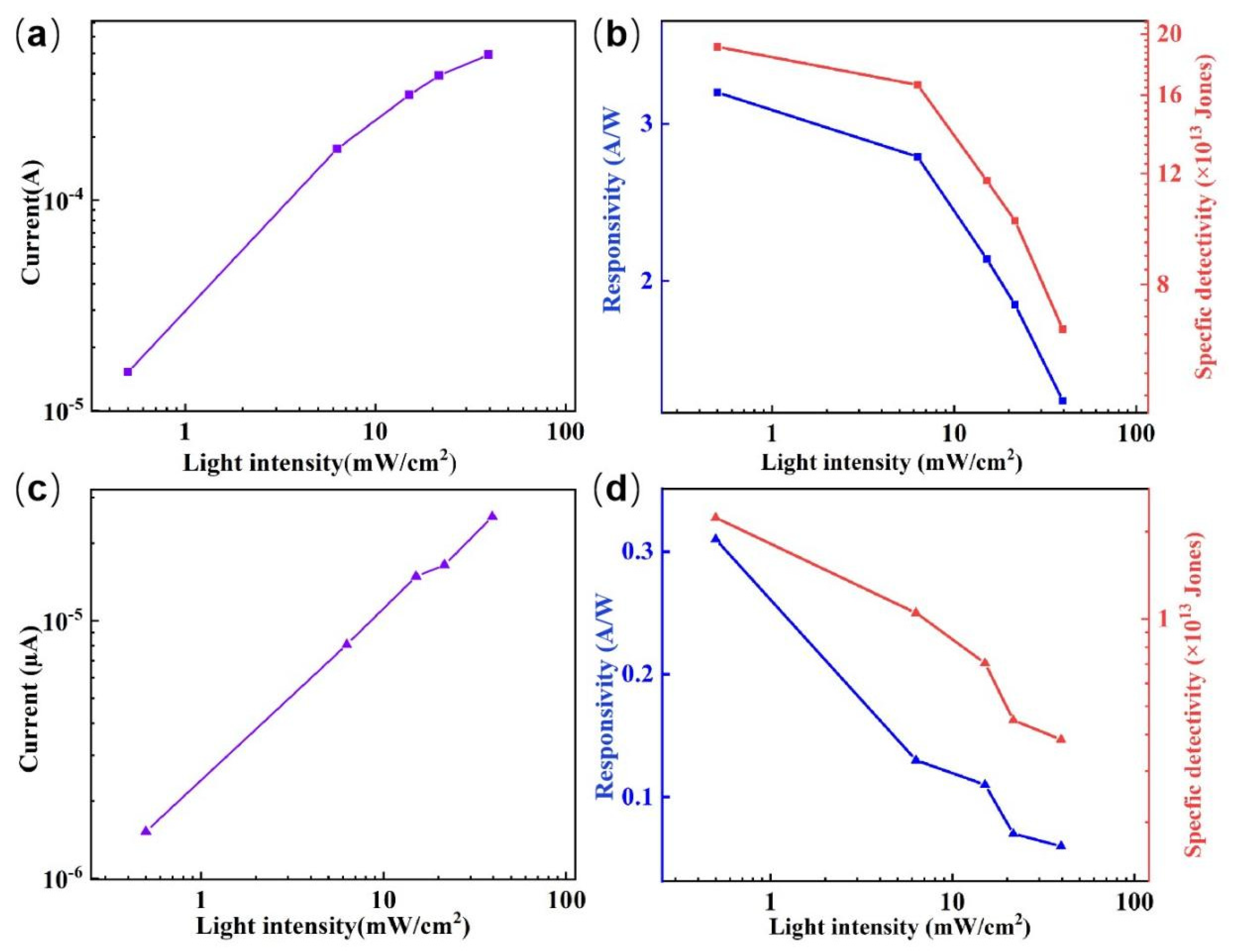
4/textured Si n-n heterojunction was further evaluated by analyzing its response to 650 nm (650 nm represents a central wavelength in the visible spectrum and is readily available from standard laser diodes) light at varying intensities, with key figures of merit including photocurrent, responsivity, and specific detectivity.
Figure 4a shows the dependence of the net photocurrent (
Iph =
Ilight − Idark) on incident light intensity. A clear monotonic increase in
Iph is observed as the illumination power rises, indicating efficient photon absorption and carrier generation. Specifically, when the light intensity increases from 0.5 mW/cm
2 to 39.5 mW/cm
2, the photocurrent rises from 15.4 μA to 506.2 μA, reflecting high sensitivity and a strong signal response. To assess the linearity of the photoresponse, the relationship between
Iph and incident power (
P) was fitted to the power-law expression
Iph ∝
Pθ, where θ is the linearity exponent. The fitted θ value of approximately 0.81, which is less than the ideal linear case (θ = 1), suggests sub-linear behavior, likely due to the presence of trap states within the bandgap. These traps, possibly located near the valence or conduction band edges, can temporarily capture photogenerated carriers, delaying their release and contributing to non-ideal recombination dynamics [
38]. Despite this, the high photocurrent magnitude and broad dynamic range underscore the device’s strong potential for practical photodetection applications. To comprehensively assess the performance of g-C
3N
4/textured Si n-n heterojunction photodetector, the responsivity (
R) and specific detectivity (
D*) were calculated using the following standard equations [
39,
40]:
where
Iph is the net photocurrent,
P represents the incident light intensity,
q is the elementary charge (1.6 × 10
−19 C),
S is the active area of the junction device (0.25 cm
2),
A is the effective illuminated area (0.01 cm
2), and
Idark is the dark current.
Figure 4b presents the variation of
R and
D* with increasing light intensity at 650 nm. Both parameters exhibit a decreasing trend as illumination intensity rises, which is attributed to enhanced carrier recombination under high photon flux—more photogenerated electrons and holes are likely to recombine non-radiatively before being collected, reducing quantum efficiency [
41]. Despite this, the device achieves impressive peak performance at low light levels. The maximum responsivity reaches 3.2 A/W, and the specific detectivity attains 1.9 × 10
14 Jones (1 Jones = 1 cm Hz
1/2W
−1) under 0.5 mW/cm
2 illumination, indicating excellent sensitivity and low noise characteristics. These values highlight the device’s strong capability for detecting weak optical signals, particularly in self-powered mode, making it highly suitable for energy-efficient photodetection applications.
Compared to planar silicon, textured silicon features micro- or nanoscale surface structures that significantly reduce light reflection and enhance light trapping through multiple scattering and absorption. This increased optical path length boosts photon harvesting efficiency. Moreover, the enlarged surface area facilitates improved charge separation and transport at the interface. Consequently, leveraging the synergistic effects of surface texturing can greatly enhance the overall performance of optoelectronic devices, such as solar cells and photodetectors [
42]. To highlight the advantages of the g-C
3N
4/textured Si n-n heterojunction, a control device based on g-C
3N
4/planar Si was fabricated using identical materials and processing conditions. The photodetection performance of this planar heterojunction is shown in
Figure 4c,d. Under 650 nm illumination, the photocurrent increases from 1.5 μA to 25.3 μA as the light intensity rises from 0.5 mW/cm
2 to 39.5 mW/cm
2. Concurrently, the responsivity decreases from 0.31 A/W to 0.06 A/W, and the specific detectivity drops from 2.23 × 10
13 to 3.85 × 10
12 Jones, consistent with the trend observed in the textured device due to increased carrier recombination at higher intensities. Furthermore, the reduction in
R and
D* at high intensities is consistent with the band alignment at the g-C
3N
4/Si interface, where trap states near the junction contribute to recombination, as evidenced by the ideality factor of 1.41. This underscores the importance of interface engineering for optimizing high-intensity performance. Moreover, a direct comparison reveals that both
R and
D* of theg-C
3N
4/textured Si device are approximately one order of magnitude higher than those of the planar counterpart under the same illumination conditions (
Table 1). All photodetection measurements were performed using calibrated light sources with intensities normalized to the same standard values for direct comparison. This significant enhancement is primarily attributed to the textured surface, which effectively reduces optical reflection and promotes light trapping through multiple scattering events. The resulting increase in photon absorption enhances carrier generation, leading to superior photoresponse. This demonstrates that surface texturing plays a critical role in boosting the efficiency of heterojunction photodetectors by maximizing light utilization and improving overall device performance [
43]. Our future studies will focus on systematically optimizing key fabrication parameters, such as the g-C
3N
4 film thickness and Si texturing conditions, to further enhance device performance and understand their precise effects.
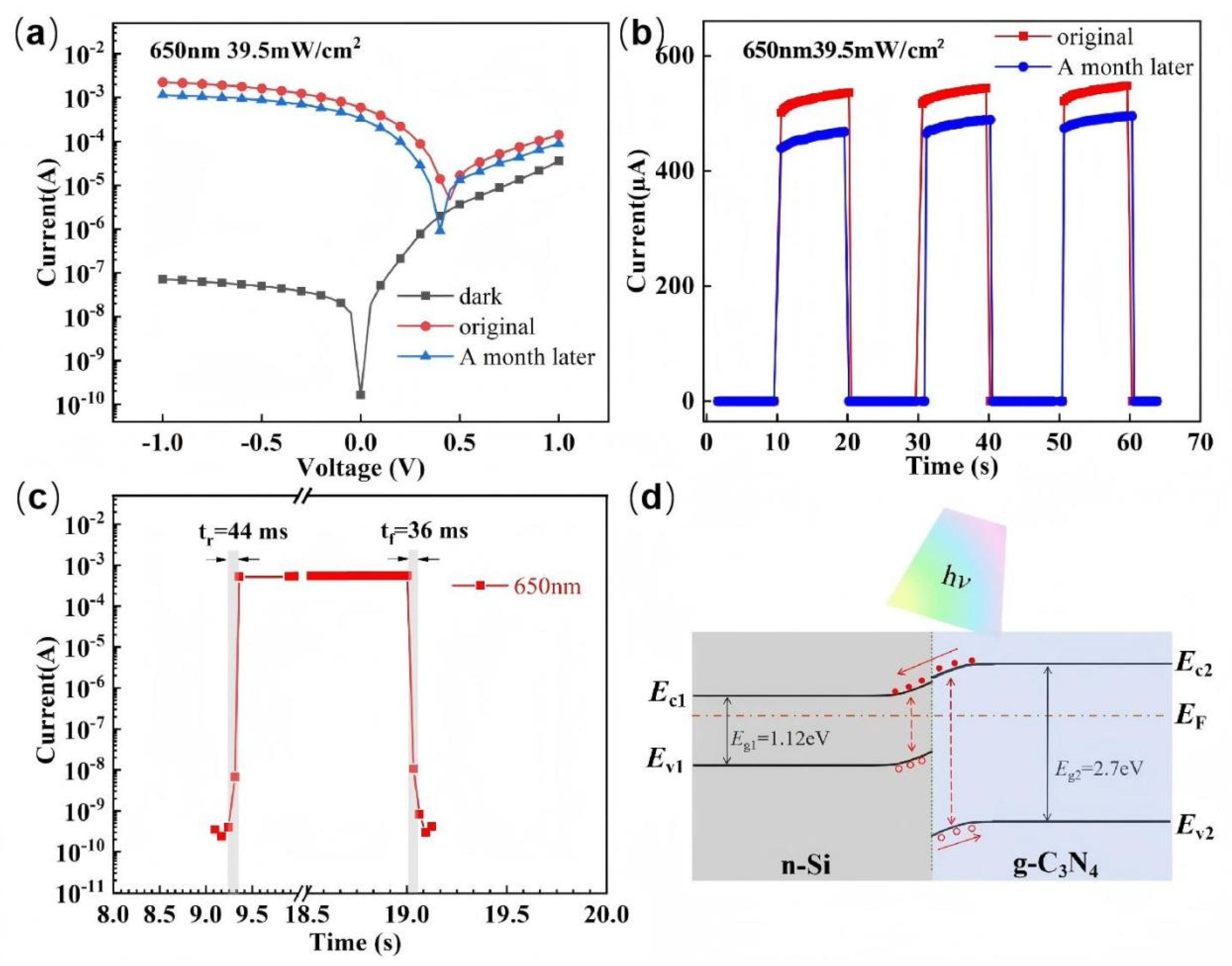
Long-term stability is a crucial requirement for photodetectors in real-world applications. To assess the ambient stability of the fabricated g-C
3N
4/textured Si n-n heterojunction, the device was stored in ambient air at room temperature without any protective encapsulation for one month. Remarkably, as shown in
Figure 5,b, the device retains strong photovoltaic behavior in self-powered mode, generating a clear photocurrent upon illumination and exhibiting fast, repeatable switching between dark and light states with sharp response transients. This indicates that the core heterojunction functionality remains intact. However, a modest 8% reduction in photocurrent magnitude is observed after aging, which shows a slow degradation. This decay is likely due to surface adsorption of moisture and oxygen, slight oxidation of the g-C
3N
4 layer, native oxide growth on the Si surface affecting interface quality, and potential contact degradation. These factors may increase recombination and reduce carrier collection efficiency. In future studies, device stability will be enhanced through encapsulation or surface passivation techniques.
Figure 5c shows a single cycle of the time-resolved photoresponse of the as-fabricated g-C
3N
4/textured Si n-n heterojunction photodetector under 650 nm illumination. From this transient curve, a rise time of 44 ms and a fall time of 36 ms are extracted, calculated based on the standard 10% to 90% current change criteria. The fast response dynamics are primarily attributed to the strong built-in electric field at the heterojunction interface, which efficiently separates photo-generated electron-hole pairs and accelerates carrier transport, minimizing recombination losses and enabling rapid device switching. To gain deeper insight into the self-powered photodetection mechanism of the g-C
3N
4/textured Si n-n heterojunction, the energy band alignment at the interface is analyzed and illustrated in
Figure 5d. The heterojunction forms together with the mismatch in electronic energy levels between n-type g-C
3N
4 and n-type Si, specifically the valence band maximum (
Ev), conduction band minimum (
Ec), and Fermi level (
Ef) Upon intimate contact, electrons diffuse from the material with the higher Fermi level (n-Si) to the one with the lower Fermi level (g-C
3N
4) to establish thermal equilibrium. This charge transfer induces interfacial band bending: the energy bands in g-C
3N
4 bend downward, while those in n-Si bend upward, creating a built-in electric field directed from n-Si to g-C
3N
4 across the junction. Under illumination, electron-hole pairs are generated primarily at or near the interface. The built-in field then efficiently separates these photogenerated carriers; electrons are accelerated toward the n-Si side, while holes drift toward the g-C
3N
4 side. This directional charge transport enables rapid carrier collection at the respective electrodes without requiring external bias, resulting in a significant photocurrent. The efficient separation and suppression of recombination due to the strong internal field are key to the device’s high-performance self-powered operation.