

Effect of Sputtering Process Parameters on Physical Properties and Electron Emission Level of Titanium Nitride Films


Abstract
1. Introduction
2. Results and Discussion
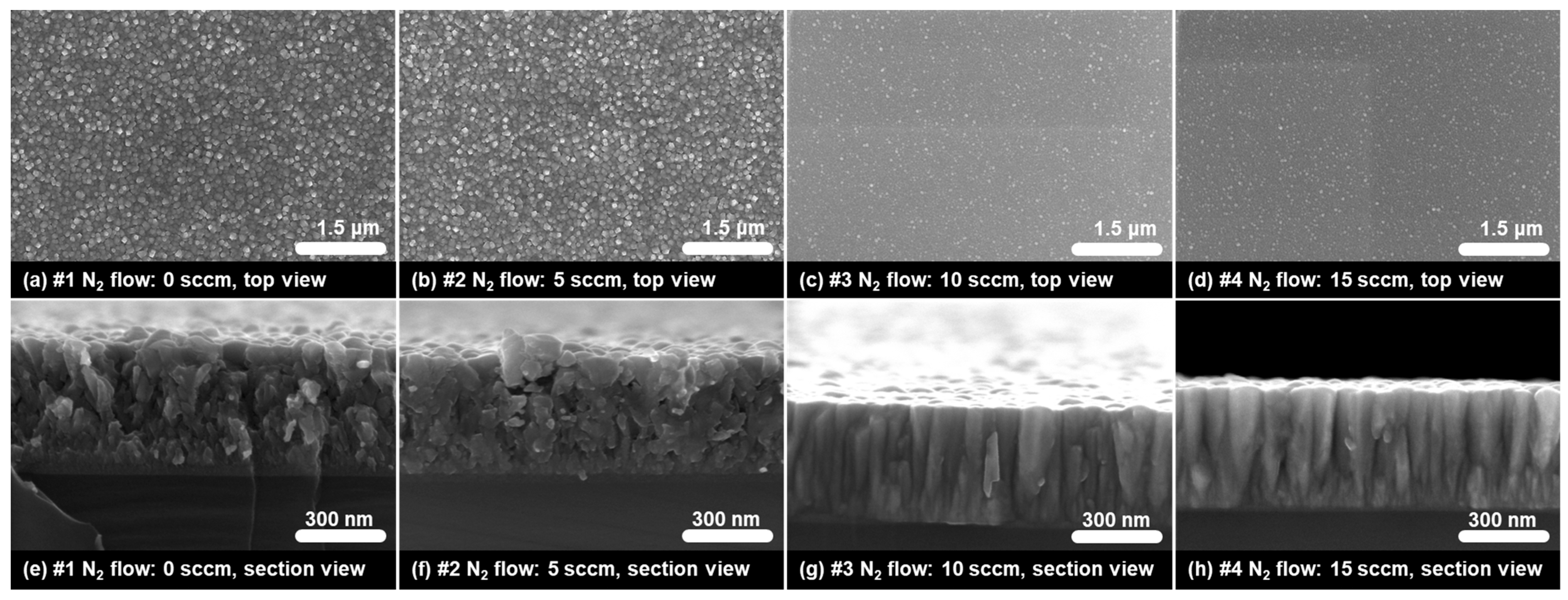
2.1. Morphology Characterization of TiN Films
2.2. Composition Characterization of TiN Films
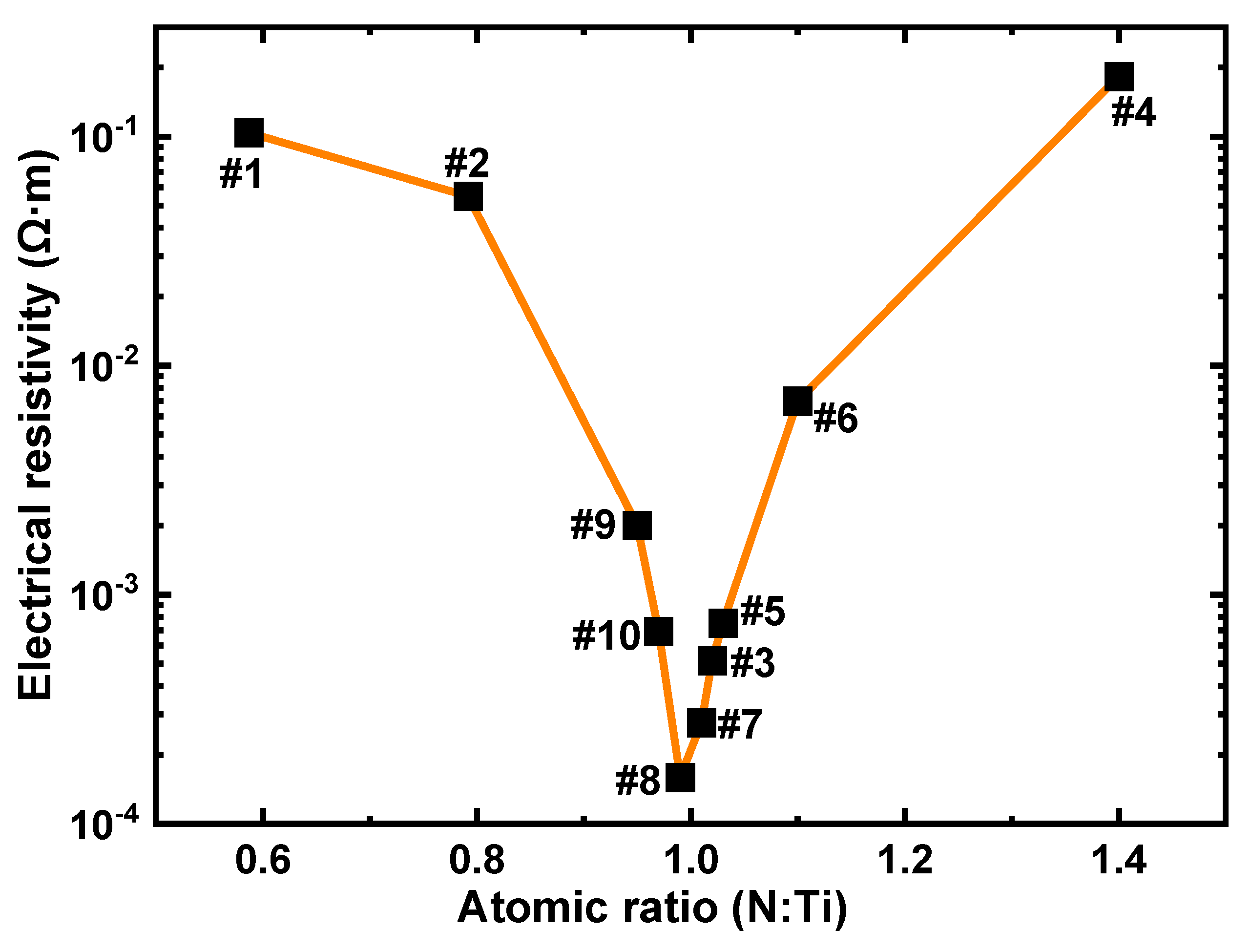
2.3. Characterization of Electrical Resistivity Property for the TiN Films
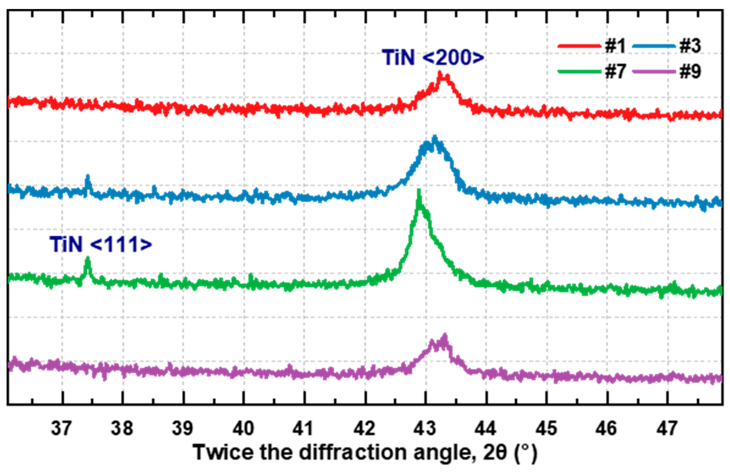
2.4. Crystal Structure Characterization of TiN Films
2.5. Secondary Electron Emission Properties of TiN Films
3. Materials and Methods
3.1. TiN Film Preparation
3.2. Physical Characterization Methods
4. Conclusions
Author Contributions
Funding
Institutional Review Board Statement
Informed Consent Statement
Data Availability Statement
Conflicts of Interest
References
- Vasu, K.; Krishna, M.G.; Padmanabhan, K.A. Substrate temperature dependent structure and composition variations in RF magnetron sputtered titanium nitride thin film. Appl. Surf. Sci. 2011, 257, 3069–3074. [Google Scholar] [CrossRef]
- Gavarini, S.; Bes, R.; Millard-Pinard, N.; Cardinal, S.; Peaucelle, C.; Perrat-Mabilon, A.; Garnier, V.; Gaillard, C. A comparative study of TiN and TiC: Oxidation resistance and retention of xenon at high temperature and under degraded vacuum. J. Appl. Phys. 2011, 109, 014906. [Google Scholar] [CrossRef]
- White, N.; Campbell, A.L.; Grant, J.T.; Pachter, R.; Eyink, K.; Jakubiak, R.; Martinez, G.; Ramana, C.V. Surface/interface analysis and optical properties of RF sputter-deposited nanocrystalline titanium nitride thin films. Appl. Surf. Sci. 2014, 292, 74–85. [Google Scholar] [CrossRef]
- Popović, M.; Novaković, M.; Mitrić, M.; Zhang, K.; Bibic, N. Structural, optical and electrical properties of argon implanted TiN thin films. Int. J. Refract. Met. Hard Mater. 2015, 48, 318–323. [Google Scholar] [CrossRef]
- Chaudhry, A.U.; Mansoor, B.; Mungole, T.; Ayoub, G.; Field, D.P. Corrosion mechanism in PVD deposited nano-scale titanium nitride thin film with intercalated titanium for protecting the surface of silicon. Electrochim. Acta 2018, 264, 69–82. [Google Scholar] [CrossRef]
- Patsalas, P.; Kalfagiannis, N.; Kassavetis, S. Optical Properties and Plasmonic Performance of Titanium Nitride. Materials 2015, 8, 3128–3154. [Google Scholar] [CrossRef]
- Chin, Y.L.; Chou, J.C.; Lei, Z.C.; Sun, T.P.; Chung, W.Y.; Hsiung, S.K. Titanium nitride membrane application to extended gate field effect transistor pH sensor using VLSI technology. Jpn. J. Appl. Phys. 2002, 40 Pt 1, 6311–6315. [Google Scholar] [CrossRef]
- Lackner, J.M. Industrially-scaled large-area and high-rate tribological coating by Pulsed Laser Deposition. Surf. Coat. Technol. 2005, 200, 1439–1444. [Google Scholar] [CrossRef]
- Wang, D.; Mao, Z.S.; Ye, Z.; Cai, Y.H.; Li, Y.; He, Y.N.; Qi, K.C.; Xu, Y.N.; Jia, Q.Q. Ultralow electron emission yield achieved on alumina ceramic surfaces and its application in multipactor suppression. J. Phys. D Appl. Phys. 2022, 55, 455301. [Google Scholar] [CrossRef]
- Michizono, S.; Kinbara, A.; Saito, Y.; Yamaguchi, S.; Anami, S.; Matuda, N. TiN film coatings on alumina radio frequency windows. J. Vac. Sci. Technol. A 1992, 10, 1180–1184. [Google Scholar] [CrossRef]
- Ruiz, A.; Román, E.; Lozano, P.; García, M.; Galán, L.; Montero, I.; Raboso, D. UHV reactive evaporation growth of titanium nitride thin films, looking for multipactor effect suppression in space applications. Vacuum 2007, 81, 1493–1497. [Google Scholar] [CrossRef]
- Gascon, N.; Dudeck, M.; Barral, S. Wall material effects in stationary plasma thrusters. I. Parametric studies of an SPT-100. Phys. Plasmas. 2003, 10, 4123–4136. [Google Scholar] [CrossRef]
- LeClair, P.; Berera, G.P.; Moodera, J.S. Titanium nitride thin films obtained by a modified physical vapor deposition process. Thin Solid Films 2000, 376, 9–15. [Google Scholar] [CrossRef]
- Huang, N.; Wan, G.J.; Leng, Y.; Leng, Y.X.; Sun, H.; Yang, P.; Chen, J.Y.; Wang, J.; Chu, P.K. Deformation behavior of titanium nitride film prepared by plasma immersion ion implantation and deposition. Surf. Coat. Technol. 2002, 156, 170–175. [Google Scholar] [CrossRef]
- Popović, M.; Novaković, M.; Traverse, A.; Zhang, K.; Bibic, N.; Hofsaess, H.; Lieb, K.P. Modifications of reactively sputtered titanium nitride films by argon and vanadium ion implantation: Microstructural and opto-electric properties. Thin Solid Films 2013, 531, 189–196. [Google Scholar] [CrossRef]
- Şerban, V.A.; Roşu, R.A.; Bucur, A.I.; Pascu, D.R. Deposition of titanium nitride layers by electric arc—Reactive plasma spraying method. Appl. Surf. Sci. 2013, 265, 245–249. [Google Scholar] [CrossRef]
- Ingo, G.M.; Kaciulis, S.; Mezzi, A.; Valente, T.; Casadei, F.; Gusmano, G. Characterization of composite titanium nitride coatings prepared by reactive plasma spraying. Electrochim. Aata 2005, 50, 4531–4537. [Google Scholar] [CrossRef]
- Akkan, C.K.; May, A.; Hammadeh, M.; Abdul-Khaliq, H.; Aktas, O.C. Matrix shaped pulsed laser deposition: New approach to large area and homogeneous deposition. Appl. Surf. Sci. 2014, 302, 149–152. [Google Scholar] [CrossRef]
- Chen, C.; Ong, P.P.; Wang, H. Fabrication of TiN thin film by shadow-masked pulsed laser deposition. Thin Solid Films 2001, 382, 275–279. [Google Scholar] [CrossRef]
- Phani, A.R.; Krzanowski, J.E. Preferential growth of Ti and TiN films on Si(111) deposited by pulsed laser deposition. Appl. Surf. Sci. 2001, 174, 132–137. [Google Scholar] [CrossRef]
- Obata, K.; Sugioka, K.; Takai, H.; Midorikawa, K. TiN growth on Si(100) by pulsed laser deposition using homogenized KrF excimer laser beam. Appl. Surf. Sci. 1999, 138, 335–339. [Google Scholar] [CrossRef]
- Park, B.H.; Kim, Y.I.; Kim, K.H. Effect of silicon addition on microstructure and mechanical property of titanium nitride film prepared by plasma-assisted chemical vapor deposition. Thin Solid Films 1999, 348, 210–214. [Google Scholar] [CrossRef]
- Merie, V.; Pustan, M.; Negrea, G.; Birleanu, C. Research on titanium nitride thin films deposited by reactive magnetron sputtering for MEMS applications. Appl. Surf. Sci. 2015, 358, 525–532. [Google Scholar] [CrossRef]
- Cheng, H.E.; Wen, Y.W. Correlation between process parameters, microstructure and hardness of titanium nitride films by chemical vapor deposition. Surf. Coat. Technol. 2004, 179, 103–109. [Google Scholar] [CrossRef]
- Xiao, S.; Lungu, C.P.; Takai, O. Comparison of TiN deposition by rf magnetron sputtering and electron beam sustained arc ion plating. Thin Solid Films 1998, 334, 173–177. [Google Scholar] [CrossRef]
- Schmid, P.E.; Sato Sunaga, M.; Levy, F. Optical and electronic properties of sputtered TiNx thin films. J. Vac. Sci. Technol. A 1998, 16, 2870–2875. [Google Scholar] [CrossRef]
- Tony, L.; Selvam, I.P.; Potty, S.N. Composition tunablity and correlated property analysis of titanium nitride films for plasmonic applications. Ceram. Int. 2024, 50, 13185–13195. [Google Scholar] [CrossRef]
- Samanta, A.; Chattaraj, A.; Srivastava, S.; Walczak, L.; Sagdeo, A.; Kanjilal, A. Revealing plasmonic TiN films with low power radio-frequency magnetron sputtering technique. Thin Solid Films 2025, 811, 140603. [Google Scholar] [CrossRef]
- Michizono, S.; Saito, Y.; Suharyanto; Yamano, Y.; Kobayashi, S. Estimation of surface charges on dielectric materials for high power rf windows. Appl. Surf. Sci. 2009, 256, 950–953. [Google Scholar] [CrossRef]
- Suharyanto; Yamano, Y.; Kobayashi, S.; Michizono, S.; Saito, Y. Secondary electron emission and surface charging evaluation of alumina ceramics and sapphire. IEEE Trans. Dielectr. Electr. Insul. 2006, 13, 72–78. [Google Scholar] [CrossRef]
- Michizono, S.; Saito, Y.; Suharyanto; Yamano, Y.; Kobayashi, S. Surface characteristics and electrical breakdown of alumina materials. Vacuum 2007, 81, 762–765. [Google Scholar] [CrossRef]
- Montero, I.; Mohamed, S.H.; García, M.; Galán, L.; Raboso, D. Effect of surface reactions of low-energy carbon ions on the secondary electron emission of TiN:O thin films. J. Appl. Phys. 2007, 101, 113306. [Google Scholar] [CrossRef]
- Nagakura, S.; Kusunoki, T.; Kakimoto, F.; Hirotsu, Y. Lattice parameter of the non-stoichiometric compound TiNx. J. Appl. Crystallogr. 1975, 8, 65–66. [Google Scholar] [CrossRef]
- Spengler, W.; Kaiser, R.; Christensen, A.N.; Mullervogt, G. Raman scattering, superconductivity, and phonon density of states of stoichiometric and nonstoichiometric TiN. Phys. Rev. B 1978, 17, 1095–1101. [Google Scholar] [CrossRef]
- Lemperière, G.; Poitevin, J.M. Influence of the nitrogen partial-pressure on the properties of DC-sputtered titanium and titanium nitride films. Thin Solid Films 1984, 111, 339–349. [Google Scholar] [CrossRef]
- Soriano, L.; Abbate, M.; Pen, H.; Prieto, P.; Sanz, J.M. The electronic structure of TiN and VN: X-ray and electron spectra compared to band structure calculations. Solid State Commun. 1997, 102, 291–296. [Google Scholar] [CrossRef]
- Patsalas, P.; Logothetidis, S. Optical, electronic, and transport properties of nanocrystalline titanium nitride thin films. J. Appl. Phys. 2001, 90, 4725–4734. [Google Scholar] [CrossRef]
- Lengauer, W. Properties of bulk Delta-TiN1−x prepared by nitrogen diffusion into titanium metal. J. Alloys Copmd. 1992, 186, 293–307. [Google Scholar] [CrossRef]
- Hojo, J.; Iwamoto, O.; Maruyama, Y.; Kato, A. Defect structure, thermal and electrical properties of Ti nitride and V nitride powders. J. Less Common Met. 1977, 53, 265–276. [Google Scholar] [CrossRef]
- Delfino, M.; Fair, J.A.; Hodul, D. X-ray photoemission spectra of reactively sputtered TiN. J. Appl. Phys. 1992, 71, 6079–6085. [Google Scholar] [CrossRef]
- Lian, Z.X.; Xu, Y.N.; Meng, X.C.; Wang, D.; Chen, J.X.; Qi, K.C.; He, Y.N. Secondary electron emission reduction from boron nitride composite ceramic surfaces by the artificial microstructures and functional coating. J. Phys. D Appl. Phys. 2024, 57, 315304. [Google Scholar] [CrossRef]
- Yao, L.; Ouyang, L.J.; Wang, D.; Chen, J.X.; He, Y.N.; Xu, Y.N. Modulation of secondary electron emission from boron nitride composite ceramics. High Volt. Eng. 2023, 49, 3848–3855. [Google Scholar] [CrossRef]
- Lian, Z.X.; Wang, D.; Zhu, X.P.; He, Y.N. High-performance microchannel plates based on atomic layer deposition for the preparation of functional layers. J. Phys. D Appl. Phys. 2025, 58, 115106. [Google Scholar] [CrossRef]


| Sample No. | Thickness (nm) | Depositing Velocity (nm/min) | Atomic Ratio (N:Ti) |
|---|---|---|---|
| #1 | 446 | 2.47 | 0.587 |
| #2 | 389 | 2.16 | 0.792 |
| #3 | 373 | 2.07 | 1.02 |
| #4 | 355 | 1.97 | 1.40 |
| #5 | 396 | 2.20 | 1.03 |
| #6 | 422 | 2.34 | 1.10 |
| #7 | 459 | 2.55 | 1.01 |
| #8 | 394 | 2.19 | 0.991 |
| #9 | 377 | 2.09 | 0.948 |
| #10 | 384 | 2.13 | 0.972 |
| Sample No. | Square Resistance (Ω/□) | Thickness (nm) | Electrical Resistivity (Ω·m) |
|---|---|---|---|
| #1 | 2.33 × 10⁵ | 446 | 1.04 × 10⁻¹ |
| #2 | 1.41 × 10⁵ | 389 | 5.48 × 10⁻² |
| #3 | 1.38 × 10³ | 373 | 5.15 × 10⁻⁴ |
| #4 | 5.15 × 10⁵ | 355 | 1.83 × 10⁻¹ |
| #5 | 1.90 × 10³ | 396 | 7.52 × 10⁻⁴ |
| #6 | 1.66 × 10⁴ | 422 | 7.01 × 10⁻³ |
| #7 | 6.01 × 10² | 459 | 2.76 × 10⁻⁴ |
| #8 | 4.04 × 10² | 394 | 1.59 × 10⁻⁴ |
| #9 | 5.33 × 10³ | 377 | 2.01 × 10⁻³ |
| #10 | 1.80 × 10³ | 384 | 6.91 × 10⁻⁴ |
| Sample No. | N2:Ar (sccm) | Sputtering Power (W) | Sputtering Pressure (Pa) |
|---|---|---|---|
| #1 | 0:15 | 100 | 1.2 |
| #2 | 5:15 | 100 | 1.2 |
| #3 | 10:15 | 100 | 1.2 |
| #4 | 15:15 | 100 | 1.2 |
| #5 | 10:15 | 120 | 1.2 |
| #6 | 10:15 | 140 | 1.2 |
| #7 | 10:15 | 160 | 1.2 |
| #8 | 10:15 | 120 | 1.6 |
| #9 | 10:15 | 120 | 2.0 |
| #10 | 10:15 | 120 | 0.8 |
Disclaimer/Publisher’s Note: The statements, opinions and data contained in all publications are solely those of the individual author(s) and contributor(s) and not of MDPI and/or the editor(s). MDPI and/or the editor(s) disclaim responsibility for any injury to people or property resulting from any ideas, methods, instructions or products referred to in the content. |
© 2025 by the authors. Licensee MDPI, Basel, Switzerland. This article is an open access article distributed under the terms and conditions of the Creative Commons Attribution (CC BY) license (https://creativecommons.org/licenses/by/4.0/).
Share and Cite
Xia, Y.; Wang, D. Effect of Sputtering Process Parameters on Physical Properties and Electron Emission Level of Titanium Nitride Films. Inorganics 2025, 13, 201. https://doi.org/10.3390/inorganics13060201
Xia Y, Wang D. Effect of Sputtering Process Parameters on Physical Properties and Electron Emission Level of Titanium Nitride Films. Inorganics. 2025; 13(6):201. https://doi.org/10.3390/inorganics13060201
Chicago/Turabian StyleXia, Yang, and Dan Wang. 2025. "Effect of Sputtering Process Parameters on Physical Properties and Electron Emission Level of Titanium Nitride Films" Inorganics 13, no. 6: 201. https://doi.org/10.3390/inorganics13060201
APA StyleXia, Y., & Wang, D. (2025). Effect of Sputtering Process Parameters on Physical Properties and Electron Emission Level of Titanium Nitride Films. Inorganics, 13(6), 201. https://doi.org/10.3390/inorganics13060201