Article

UV–Vis Transparent Conductive Film Based on Cross-Linked Ag Nanowire Network: A Design for Photoelectrochemical Device

Research Center for Semiconductor Materials and Devices, Shaanxi University of Science and Technology, Xi’an 710021, China
*
Author to whom correspondence should be addressed.
Inorganics 2022, 10(10), 164; https://doi.org/10.3390/inorganics10100164
Submission received: 8 September 2022 / Revised: 26 September 2022 / Accepted: 29 September 2022 / Published: 2 October 2022
(This article belongs to the Special Issue Optoelectronic Properties of Metal Oxide Semiconductors)

Abstract

:
The FTO/ITO transparent conductive films currently used in photoelectrochemical devices limit performance improvement due to their low conductivity, poor flexibility, and inability to transmit UV light. Ag nanowire-based films are a very promising alternative to address these problems, and are considered to be the next generation in transparent conductive film. Here, we prepared a cross-linked nano-network composed of ultra-long Ag nanowires by a special physical template method. The obtained Ag nanowire transparent conductive film has a transmittance of over 80% in a wide range of 200 nm–900 nm, a sheet resistance as small as 5.2 Ω/sq, and can be easily transferred to various substrates without damage. These results have obvious advantages over Ag nanowire films obtained by traditional chemical methods. Considering the special requirements of photoelectrochemical devices, we have multifunctionally enhanced the film by a TiO2 layer. The heat-resistant temperature of transparent conductive film was increased from 375 °C to 485 °C, and the mechanical stability was also significantly improved. The presence of the multifunctional layer is expected to suppress the carrier recombination in self-powered photoelectrochemical devices and improve the electron diffusion in the longitudinal direction of the electrode, while serving as a seed layer to grow active materials. The high-quality Ag nanowire network and functional layer synergize to obtain a UV–Visible transparent conductive film with good light transmittance, conductivity, and stability. We believe that it can play an important role in improving the performance of photoelectrochemical devices, especially the UV devices.

1. Introduction

Transparent conductive films (TCFs) are vital in many electronic devices, including solar cells [1], touch screens [2], organic light emitting diodes (OLEDs) [3], flexible wearable devices [4], and light detectors [5]. Due to good stability, transparent conductive oxide (TCO, such as ITO (Indium Tin Oxide) and FTO (Fluorine Tin Oxide)) is most currently used in TCF fields. However, low raw material reserves, low electrical conductivity, and lack of flexibility restrict its application in many photoelectric devices. In addition, TCO films composed of wide-bandgap semiconductors have extremely poor transmittance to UV light, which makes them unable to be used in UV devices. In some solid-state detectors, TCF is usually used as electrode material or window material to protect the device or isolate it from environmental influences. In photoelectrochemical (PEC) devices (such as dye-sensitized solar cells and PEC UV detectors [6]), TCF is used as both the electrode and the encapsulation material, and the light source must pass through TCF to reach the active materials. In this case, the TCF has three functions: collecting electrons, supporting active materials, and protecting the device [7]. Therefore, most application situations require TCFs with excellent electrical conductivity, good stability, and high transmittance. Up to now, TCF used in PEC devices is basically FTO with poor performance [8,9]. For a PEC UV detector, FTO only has insufficient transmittance in the UVA band and cannot transmit deeper UV light. This seriously affects the improvement of device performance, especially the response range. At present, carbon nanotubes (CNTs) [10], graphene [11], conductive organic polymer [12], metal grids [13], and metallic nanowires [14,15] (NWs) are the main alternative materials to TCO.
Carbon-based TCFs represented by CNT have good stability and flexibility potential, but it is difficult for such films to achieve high light transmittance and electrical conductivity at the same time [16]. Organic-based TCFs have serious stability problems and find it difficult to tolerate UV light. Researchers turned their attention to metal-based TCFs. Metal materials have excellent electrical conductivity, and the formation of a hollow grid structure will enable high transmission in both UV and visible bands. Rathmell’s team chemically produced copper NWs with a length of 10 μm and thickness of 90 nm, with a sheet resistance of 15 Ω/sq, and a transmittance of 65%. Excellent chemical stability, mechanical stability, and low production cost make it suitable for using in optoelectronic devices [17]. Ana’s group produced single-layer, densely packed, and ultrathin gold NWs with photoelectrical properties comparable to ITO and graphene-based electrodes [18]. Lee et al. synthesized Ag NWs (AgNWs) with good electrical conductivity and transmittance by a simple chemical method, which could be used as a substitute for CNTs. The highly flexible and transparent metal conductor can be used on uneven surfaces and could be used in future wearable electronics [19]. Among these numerous studies, TCFs based on AgNWs have the most potential due to their excellent electrical conductivity. However, AgNWs prepared by traditional chemical methods have poor contact at the intersections due to the difficult-to-remove organics on the surface, resulting in high contact resistance. In addition, the film forming and transfer process of this method is usually complicated, and impurities may be introduced during the preparation. On the other hand, the TCF based on AgNWs has poor adhesion and stability to the substrate due to ex situ preparation and rough surface [20], and the melting point decreases sharply after nanometerization. These all adversely affect the performance of the device. Many efforts focus on studying the solution to these problems, such as preparing AgNWs by physical methods [21,22,23], embedding AgNWs into polymers [24,25,26], treating substrate surface with plasma [27], and compounding AgNWs with polymer binder [28,29]. There are also a series of reports on improving the performance of TCFs by depositing protective layers. Ni-Zn Co-doped TiO2 layers [30], ZnO-TiO2 thin films [31], and alcoholic TiCl4-treated solution [32] were all deposited by spin coating. Low cost, nontoxicity, and abundant reserves cause TiO2 to be considered as the applicable alternative material for protective layers.
Considering the good stability (including mechanical stability, chemical stability, and thermal stability) and suitability for deposition of active materials, as well as the considerable transmittance over a broad spectrum, to the best of our knowledge, we rarely see ideal AgNW-based TCF being used as the electrode of a PEC UV detector. In this work, we adopt a facile template method to prepare AgNW networks with good photoelectronic performance, easy transfer, and fewer impurities. The interconnected NW networks we prepared have ideal intersections. After transfer to quartz substrate, the AgNW TCF (AgTCF) possesses an excellent 80% optical transmittance from UV to visible region and a low sheet resistance of 5.2 Ω/sq. The performance of the electrodes was then optimized by depositing a multifunctional TiO2 layer. The protective layer with triple functions can simultaneously achieve the following functions: improving electrode stability, suppressing electron recombination, and serving as a seed layer for active materials. Under optimal experimental conditions, the AgTCF sputtered with TiO2 layer (T-AgTCF) still has high transmittance at deep UV region and a sheet resistance of 9.5 Ω/sq, and the thermal and mechanical stability were also improved.

2. Experimental Section

All chemicals are of analytical grade. The whole preparation process of AgNW-based TCFs is shown in Figure 1.

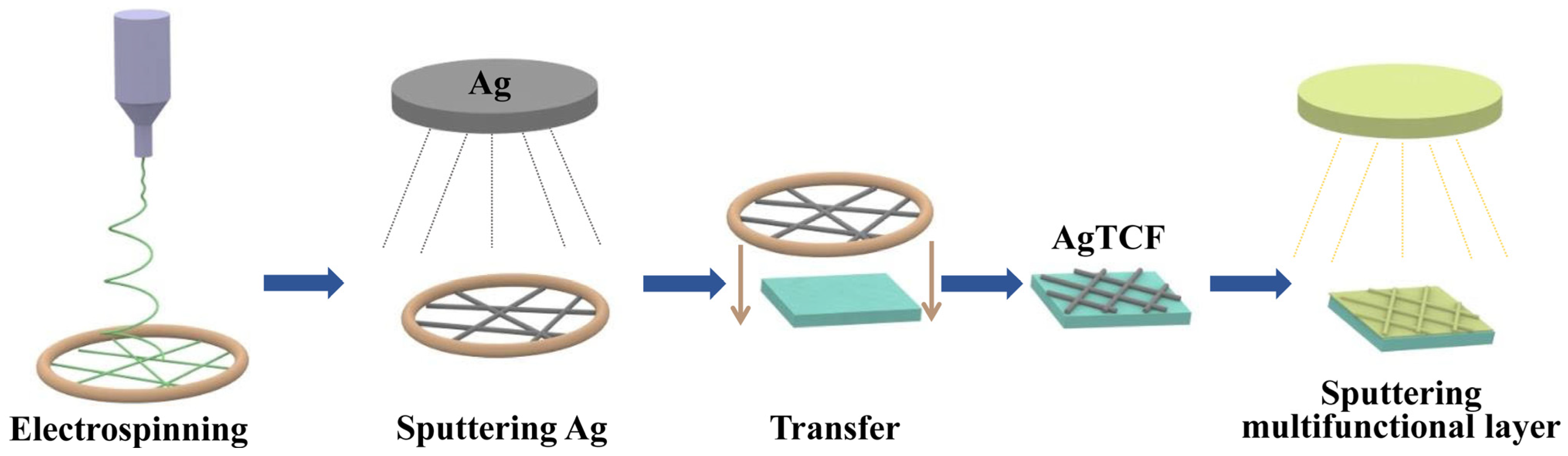
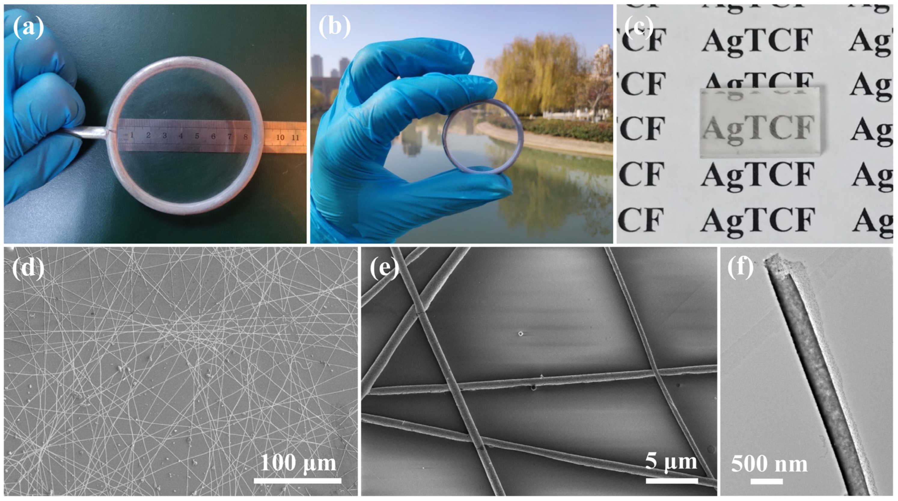
2.1. Preparation of AgTCFs Based on Interconnected AgNWs

Electrospinning is considered to be an effective method to produce polymer fibers with diameters in the range from nanoscale to micron scale [33,34]. A 0.35 g measure of Polyvinyl Pyrrolidone (PVP) was mixed in 5 mL ethanol and then magnetic-stirred for 30 min until the PVP was completely melted. The mixed solution was poured into a syringe. Then, the positive electrode of the high-voltage (15 kV) power supply was connected to the needle and the negative electrode to a vacant metal ring, maintaining a distance between the needle and the metal ring of 10 cm. The spinning process lasted for 2 min. In this way, a cross-linked network layer composed of PVP NWs is formed on the metal ring.
The metal ring was then placed as-is in a vacuum chamber to deposit a layer of Ag on the PVP nanonetwork by magnetron sputtering (Ag target, 99.99% pure), via the DC sputtering method. Before the formal sputtering, two mins of pre-sputtering was used to remove impurities from the target surface. The basic pressure was 6 × 10⁻³ mTorr, Argon (Ar) was used as reactive gas, and its flow velocity was 30 sccm. After the air flow was stable, the pre-sputtering time was set to 2 min, the power was 150 W, and the pressure was 4 mTorr. After the completion of pre-sputtering, the baffle plate was opened for formal sputtering. The working conditions of the sputtering process, including power, pressure, and time, were the same as pre-sputtering. After the sputtering was completed, the AgNWs network was transferred onto quartz glass with a drop of alcohol. This simple operation protects the AgNWs from fracture during the transfer process and enables the formation of a uniform film. The quartz substrates (14 mm × 8 mm × 2 mm) were defatted in methanol and acetone, then ultrasonically cleaned in deionized water.

2.2. Preparation of Multifunctional Layer

A Ti target (99.99% pure) was used to sputter TiO2 multifunctional layer. The prepared AgTCFs were placed into the sputtering chamber. Argon (Ar) and Oxygen (O2) were used as reaction gases with a ratio of 30 (Ar):10 (O2). The sputtering time of TiO2 layer increased from 1.5 min to 12 min, and other working conditions were the same as sputtering AgNWs.

2.3. Fabrication of TiO2 Nanoarray on the Multifunctional Layer

A 10 mL measure of deionized water, 14 mL hydrochloric acid (38% by weight), and 0.3 g tetrabutyl titanate were mixed as the precursor solution, and the mixture was stirred for 5 min. T-AgTCF (annealed in the air for 45 min at 450 °C) was put under the teflon-lined stainless-steel autoclave and the conducting surface was facing down. The hydrothermal reaction was carried out at 150 °C for 5 h. After the reaction, the autoclave was taken out after cooling to room temperature. Furthermore, the samples were rinsed with deionized water and dried in the oven.

2.4. Characterization

A four-probe semiconductor tester and TU-1901-type double-beam UV–Vis spectrophotometer was used to test the sheet resistance and transmittance, respectively.
The microstructure of the AgTCFs and T-AgTCFs were characterized by field emission scanning electron microscopy (FESEM). We adopted a KSL-1100X-S-type high-temperature sintering furnace to test the thermal stability. Some 3M scotch tape and pencils with different hardness were used to test the mechanical stability of the TCFs. The surface morphology of the samples after high-temperature sintering and mechanical test was observed by optical microscope.

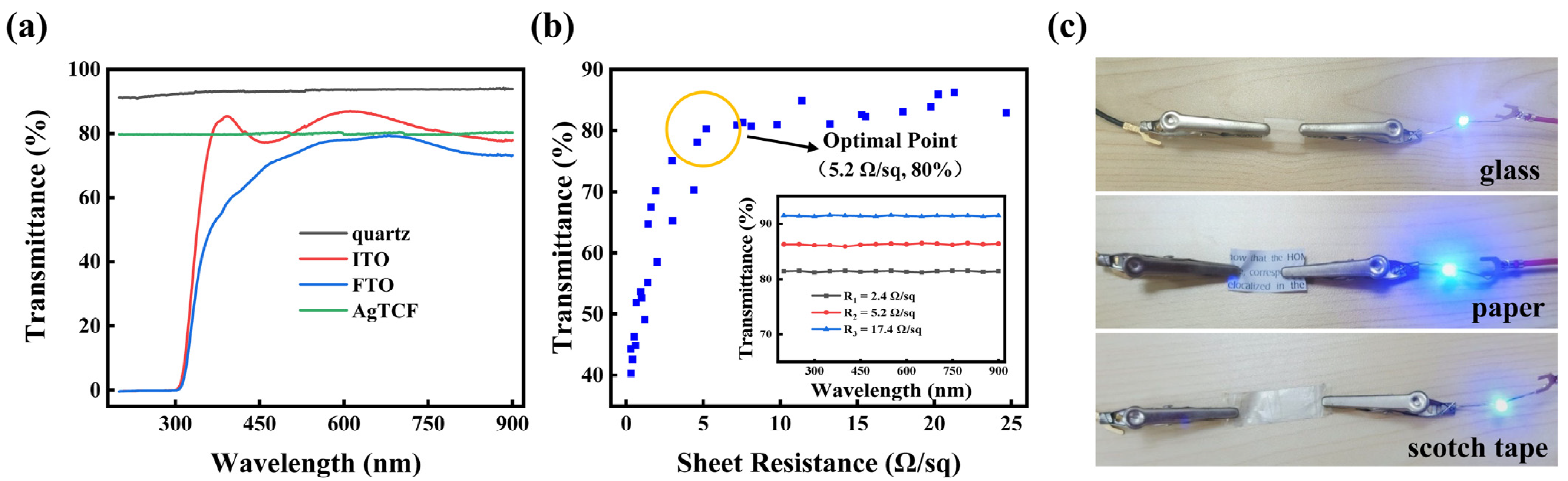
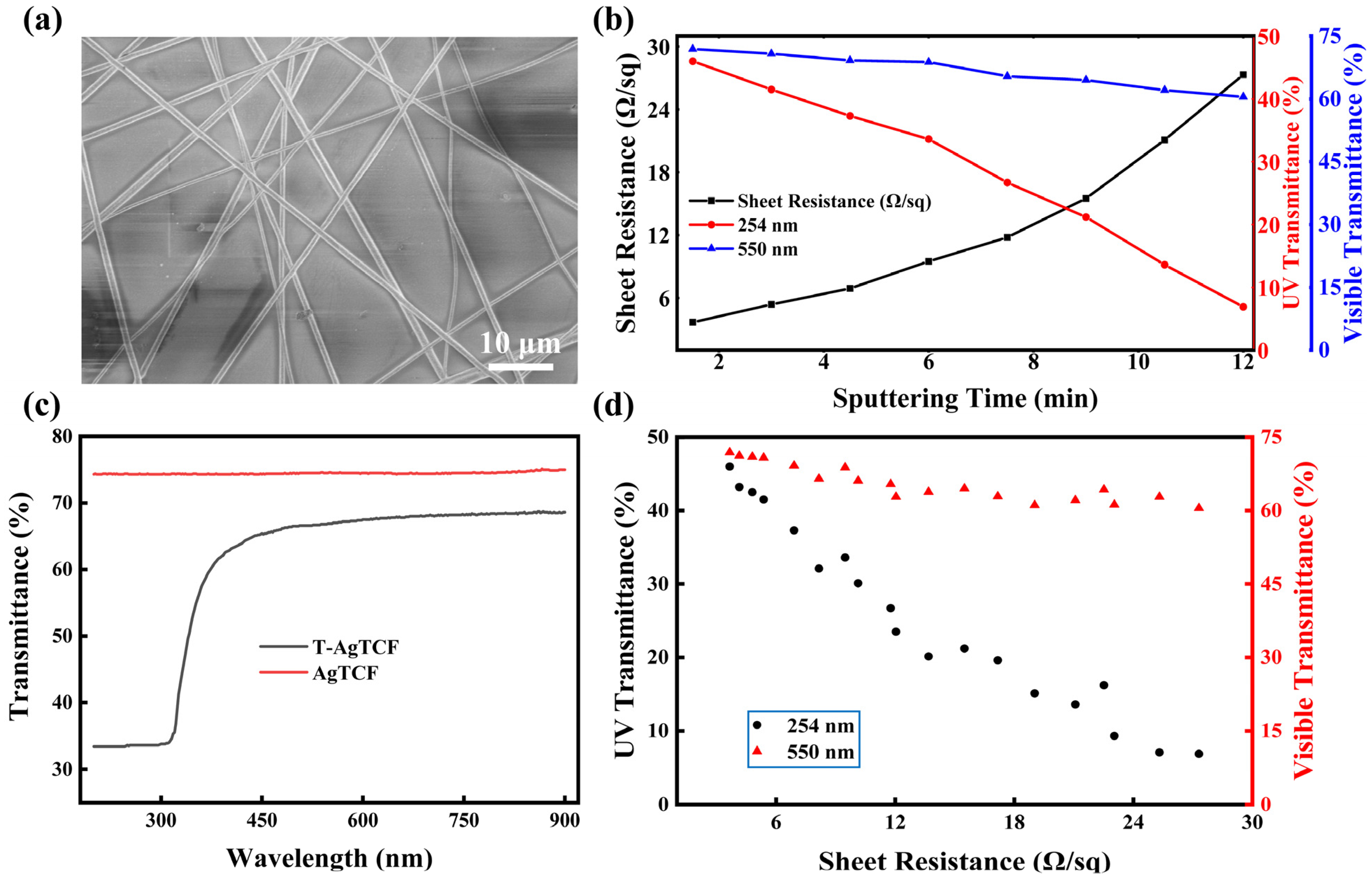
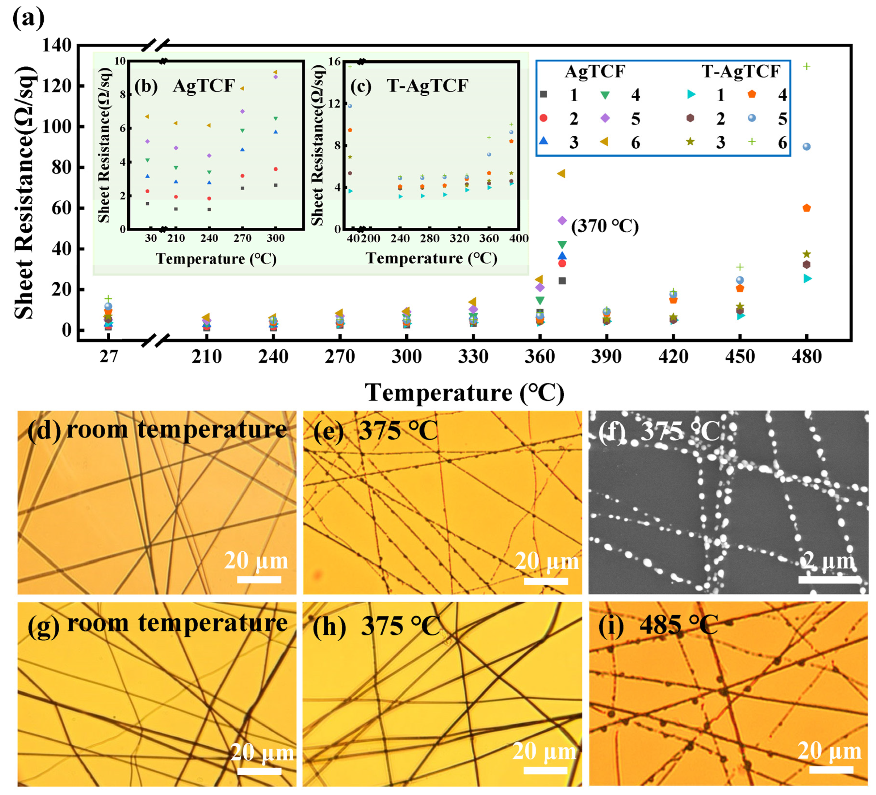
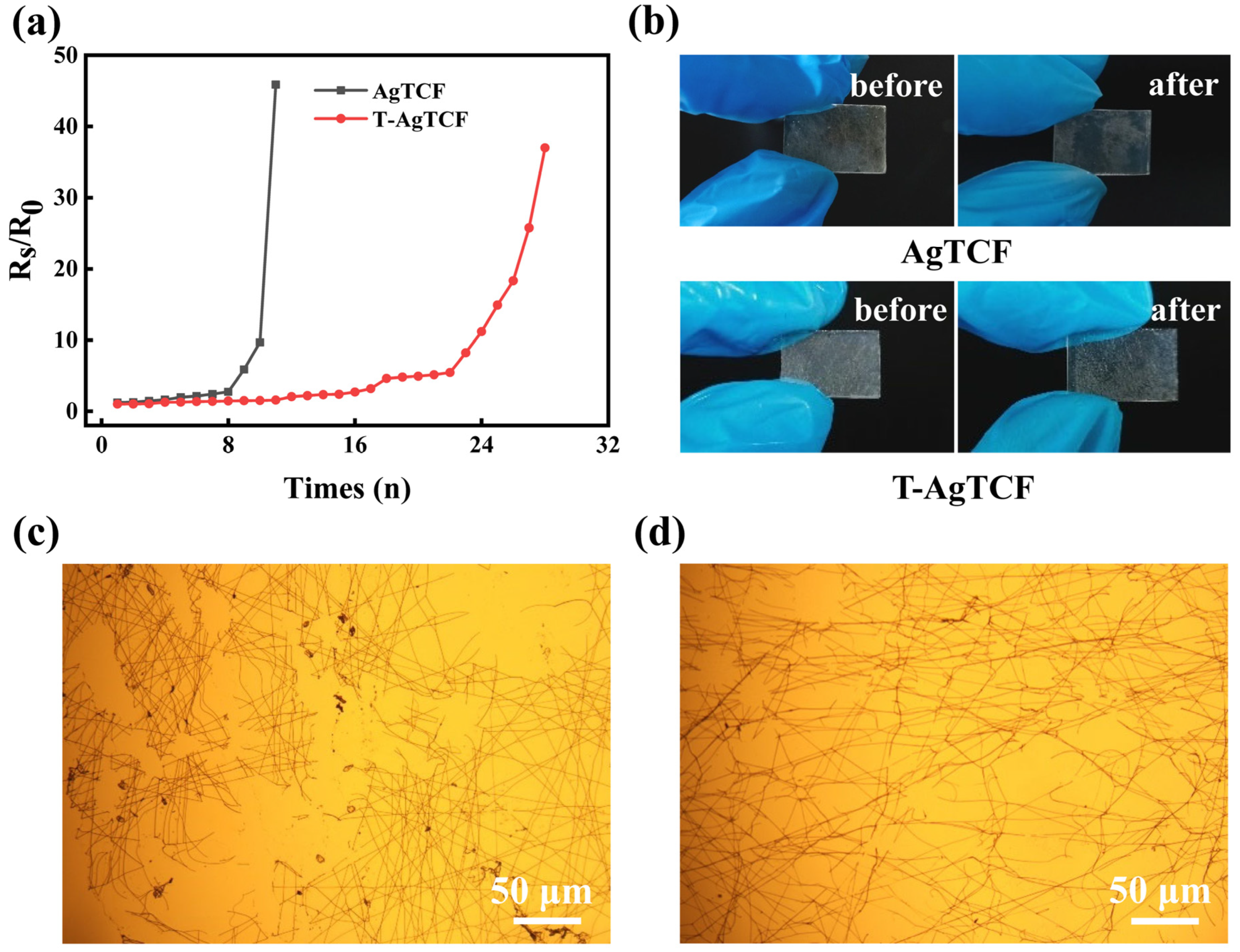
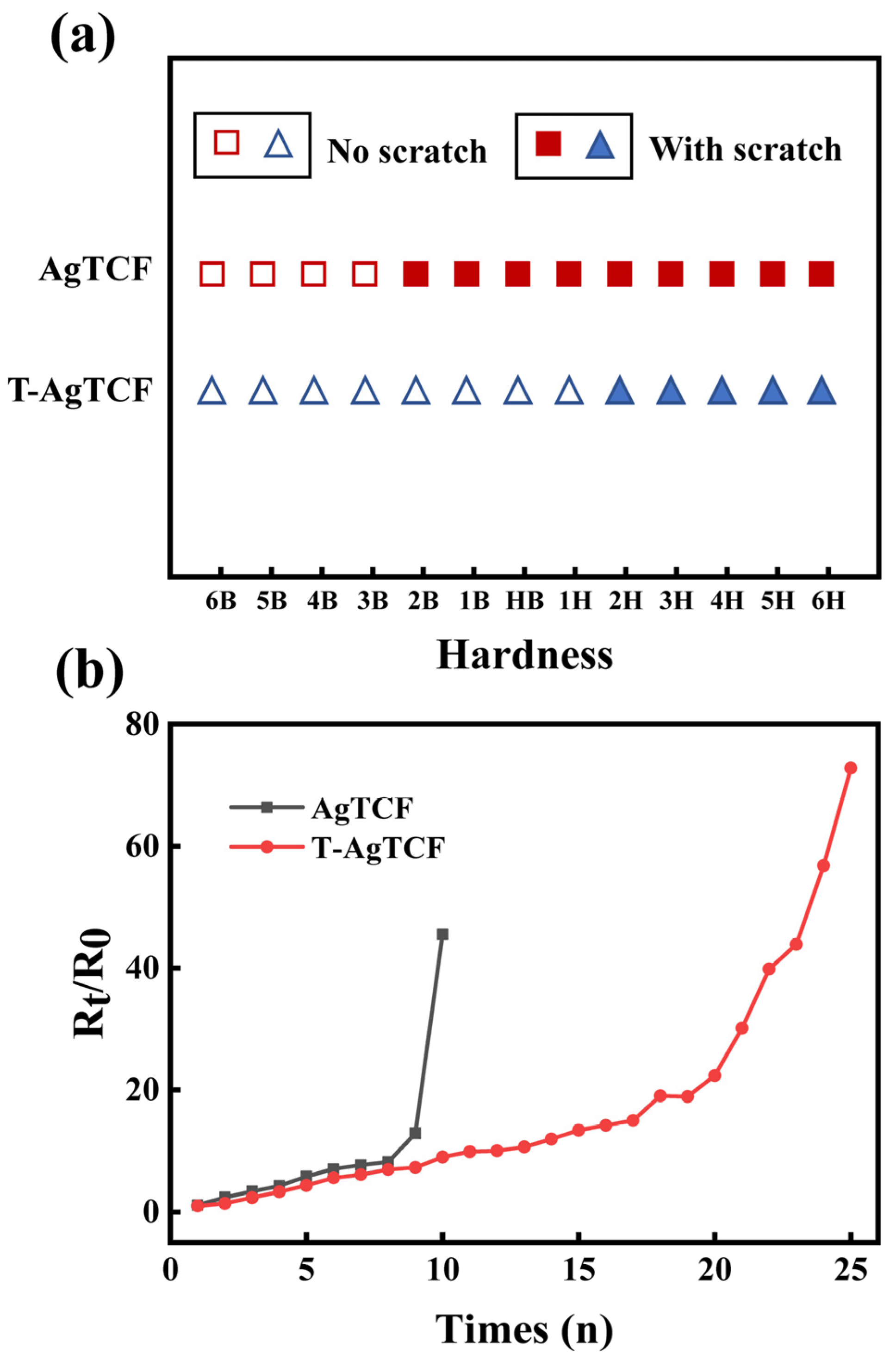
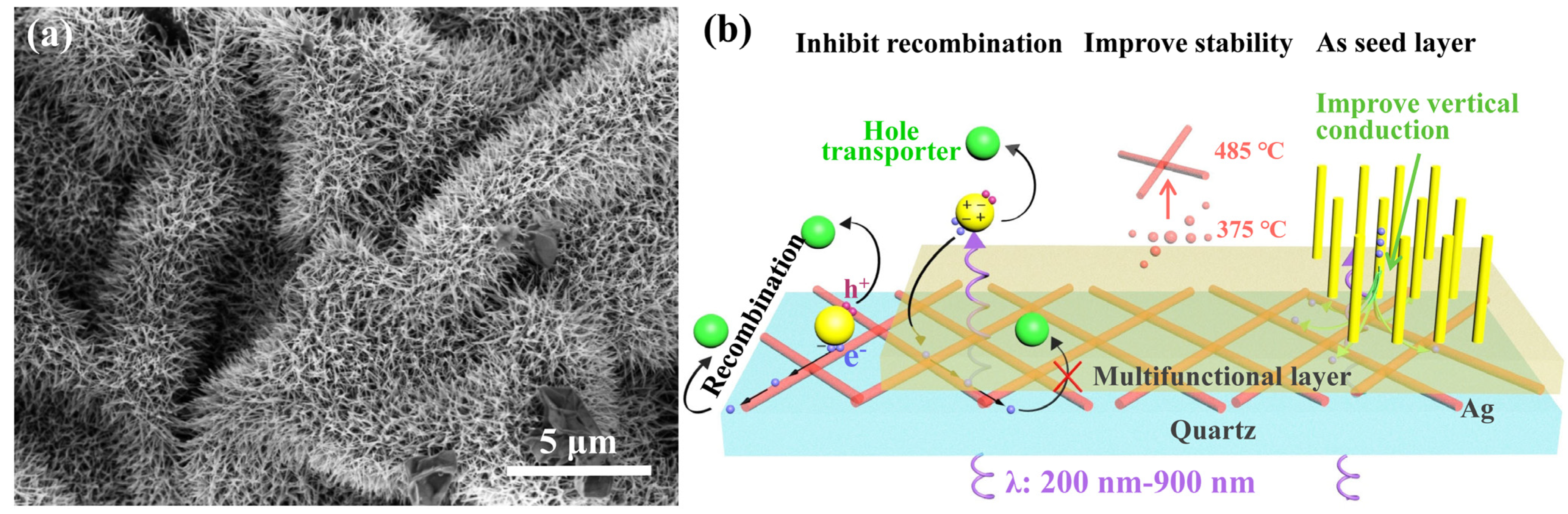
3. Results and Discussion

Electrospinning technology is usually used to prepare nanofibers of various materials. Polymer fibers containing inorganic salt ions are spun on a flat substrate, and then sintered to obtain NWs of target substances. Here, we spun bare polymer NWs onto a suspended metal ring. As shown in Figure 2a, the polymer NWs formed a uniform thin film across the ring, which had high transparency. When the scale of the film reaches more than 10 cm, it can still be self-supporting, which is very beneficial for fabrication of large-scale devices. We can adjust the density of NWs by changing the electrospinning time and the concentration of precursor. The diameter of polymer NWs is affected by electrospinning voltage, electrospinning distance, solvent volatilization rate, and polymer molecular weight. We can use different polymers to obtain the desired NW network. Considering environmental protection and low cost, we used the water-soluble PVP polymer for the entire study. Then, the obtained PVP NW network was used as a template, the entire metal ring was placed in a vacuum chamber as-is, and a layer of Ag was sputtered on the template from the top to conduct electricity. As shown in Figure 2b, the film did not change significantly after depositing the Ag layer, and still had high transparency, which was almost imperceptible at a distance (slight metallic luster can be seen under side light illumination, Figure S1). Finally, AgNW film was transferred to the substrate. Considering that it will be applied to UV detectors, we chose quartz substrates, which have high UV transmittance (Figure 2c). The SEM images of the AgNW network attached to the quartz substrate are shown in Figure 2d,e. It can be seen from Figure 2d that the AgNWs cover the substrate surface irregularly and uniformly. There are sufficient gaps between NWs to allow light of any wavelength to pass through, which is the unique advantage of metal NW-based TCFs. The density and diameter of the AgNWs have a decisive influence on the electrical conductivity and light transmission, which can be achieved by changing the polymer template. Compared with traditional chemical methods, the length of AgNWs we prepared is very large, which can even reach the order of centimeters. The diameter of AgNWs obtained from SEM images ranged from 300 nm to 1000 nm, with an average value of 626 nm (Supplementary Figure S2). Theoretically, this size of AgNWs can produce good light scattering, thereby enhancing the light absorption of PEC devices. The TEM image in Figure 2f shows the fine structure of a single AgNW. Since Ag is sputtered on the surface of the PVP NW from one side, the AgNW exhibits a half-shell-like morphology.
The transmittance curves of different TCFs are shown in Figure 3a. The conductive layers of FTO and ITO are composed of continuous wide-bandgap semiconductor oxide films which have strong absorption of UV light. Therefore, the transmittance of this kind of TCF decreases rapidly when the wavelength is lower than 400 nm, and a deep UV light with the wavelength less than 300 nm cannot be transmitted at all. The quartz glass has excellent light transmittance in a wide range from UV to visible light. After transferring the AgNW network to the quartz substrate, the overall transmittance of AgTCF decreased slightly. In general, when the thickness of metal film is more than 80 nm, it is basically opaque [35], but the hollow AgNW network we prepared allows much light to pass through from the gaps between the NWs. In the large range of 200 nm–900 nm, the light transparency of AgTCF did not fluctuate significantly, and the overall light transmittance was greater than 80%. Quartz glass produced by natural quartz sands has an absorption peak at 196 nm (The transmittance of quartz glass from 190 nm to 300 nm is shown in Figure S3). Therefore, the transmittance of AgTCF with quartz as the substrate will drop significantly when the wavelength is less than 200 nm.
It should be noted that we can achieve higher transmittance by reducing the density or diameter of the AgNWs, but this will weaken the conductivity, which is another important property of our concern. By changing the experimental conditions, we easily obtained three AgNW networks (without substrate) with different properties (as shown in the inset of Figure 3b), and the sheet resistance of the film can be as low as 2 Ω/sq when the transmittance is guaranteed to be greater than 80%. The synergistic relationship between the transmittance and sheet resistance of AgTCF is shown in Figure 3b (The transmittance was measured at 254 nm). It can be seen that the transmittance tends to saturate rapidly with an increase in the sheet resistance, and then will not increase significantly. Therefore, we can determine that the inflection point (about 80%, 5.2 Ω/sq) of the curve is the optimum performance position of AgTCF. TCFs composed of ultra-long AgNWs have incomparable advantages in electrical conductivity and flexibility. As shown in Figure 3c, we demonstrate the conductivity and flexibility of AgNWs through glass, paper, and scotch tape substrates, respectively.
The prepared AgNW-based UV–visible TCFs are very promising for PEC devices, but they still face the following drawbacks: (1) Poor stability, including thermal stability, mechanical stability, and chemical stability. Firstly, the melting point of AgNW is much lower than that of bulk Ag, which seriously affects the subsequent deposition of semiconductors. Secondly, it is difficult to form a firm contact between the AgNWs and the substrate, and the AgNWs easily peel off or break under the influence of external force. Thirdly, AgNWs are easily oxidized by sulfur in the air, forming an oxide layer that affects electron conduction. (2) The electrons collected by the Ag electrodes can easily recombined with semiconductor materials or hole transport materials [36,37]. (3) It is difficult to deposit high-quality semiconductor structures on AgNWs [38,39]. In this work, we attempt to simultaneously address the above concerns by depositing a multifunctional TiO2 layer on AgTCF by a simple magnetron sputtering method. (1) The thin layer of TiO2 can increase the adhesion of the AgNWs to the substrate while protecting the AgNWs. TiO2 has a high melting point and is expected to improve the heat resistance of the overall electrode. (2) The dense TiO2 layer can separate the AgNWs from the hole transport material, thereby effectively suppressing carrier recombination. (3) The sintered TiO2 layer can be used as a seed layer to grow TiO2 nanostructures, with good crystallinity by in situ means. However, the TiO2 layer will have an impact on light transmission and conductivity of the AgTCF.
As shown in Figure 4a, due to the film thickness being very thin, the morphology of the AgTCF did not change significantly after depositing the functional layer. We investigated the effect of film thickness (achieved by varying the sputtering time, the thickness data are listed in Table S1) on light transmittance and conductivity. We sputtered a TiO2 layer on FTO for 35 min according to the method and parameters of preparing TiO2 layer in the study. After sputtering, the FTO was cut with pliers. Through SEM observation of its section, it is found that the thickness of TiO2 layer is about 654 nm, and the sputtering rate of TiO2 is about 18.5 nm/min. As the thickness increases, the sheet resistance of the T-AgTCF increases continuously. When the sputtering time is 6 min, the sheet resistance of the sample reaches 10 Ω/sq, which is still very low. At the same time, the transmittance of the film decreases as the functional layer becomes thicker. For deep ultraviolet light (tested at 254 nm), when the sputtering time is 6 min, the transmittance of the sample is reduced to about 1/3. The detailed transmittance curve of this case is shown in Figure 4c.
The decreasing trend in the UV region is similar to that of FTO, and the transmittance does not decrease any more when the wavelength is less than 320 nm. When the sputtering time reaches 12 min, the transmittance of the sample in UV region is only 6.9%, which is no longer suitable as an electrode for UV optoelectronic devices. However, as shown in the visible region (tested at 550 nm), as sputtering time increases, the transmittance does not reduce greatly, which means it may still be used in visible photoelectronic devices. In order to obtain an accurate law, we tested a large number of samples. We plotted the sheet resistance versus transmittance data of T-AgTCF at the wavelengths of 254 nm and 550 nm (Figure 4d).
Nanomaterials possess small size and high surface free energy, which make their chemical potential much higher than that of bulk materials under the same conditions, and resulting in their melting point being far lower than that of bulk materials [40,41]. For nanomaterials with low dimensional structure, the ratio of the number of surface atoms to volume atoms increases rapidly with the decrease in size. AgNWs with large specific surface area have higher activity than the bulk Ag, which makes their thermodynamic properties very unstable. In general, the melting point of bulk Ag is 961.8 °C [42], however, the melting point of AgNW can be as low as 300 °C. The low thermal stability of AgNW limits its application in many devices requiring high-temperature annealing, such as PEC UV detectors and dye-sensitized solar cells [43]. Whereas metal oxides usually have high thermal stability, such as the melting point of bulk TiO2 being 1843 °C [44], even nanostructured TiO2 still has a high value. Therefore, the TiO2 functional layer we prepared may effectively improve the thermal stability of AgTCFs [45,46].
The sheet resistance changes in AgTCFs and T-AgTCFs under different sinter temperatures are shown in Figure 5a. In order to obtain more reliable results, we selected 12 samples with different initial conditions for thermal stability testing. (1) For AgTCF, we changed the PVP template to obtain six samples with different resistance values. When the temperature exceeds 240 °C, the sheet resistance starts to increase slowly, and the state of AgNWs does not change significantly (the enlarged data points are shown in Figure 5b, the optical photographs of the AgNWs are shown in Figure 5d). In the range of 330 °C to 370 °C, the sheet resistance increases greatly, the surface free energy of AgNWs decreases in this process, and the fracture trend begins. When AgTCFs are sintered at 370 °C for 30 min, the sheet resistance increases 10–30 times compared with that at room temperature. As the sinter temperature increases to 375 °C, the sheet resistance cannot be measured by a four-probe tester, which means the AgNWs have completely melted (Figure 5e). We tested the SEM images of AgTCF calcined at 375 °C for 60 min. As shown in Figure 5f, the AgNWs have melted and agglomerated into spheres. (2) For T-AgTCF, we obtained six samples with different resistance values by varying the thickness of TiO2 layer, and the sputtering times were 1.5 min, 3 min, 4.5 min, 6 min, 7.5 min, and 9 min, respectively. In the range of 240 °C to 330 °C, the sheet resistance of the composite TCFs has no significant change with the increase in temperature (the enlarged data points are shown in Figure 5c, and the optical photographs are shown in Figure 5g). When the temperature exceeds 330 °C, the sheet resistance of T-AgTCF starts to increase slowly. When the sinter temperature exceeds 450 °C, the sheet resistance changes greatly. Especially at 480 °C, the sheet resistance increases to about eight times that at room temperature. Increasing the sinter temperature to 485 °C, the sheet resistance cannot be measured, which indicates that the T-AgTCFs have melted. Figure 5g–i show the microstructure of T-AgTCFs at room temperature, 375 °C, and 485 °C, respectively.
To sum up, the fusing temperature of bare AgTCF is about 375 °C. After being enhanced by a TiO2 functional layer, the thermal stability of the film is obviously improved, the T-AgTCF has a longer thermal stability range, and the fusing temperature is raised to about 485 °C. The crystallization or phase transition temperature of many semiconductor materials is lower than 485 °C, so T-AgTCF is very promising for use in electrodes of related PEC devices to support active materials. It should be mentioned that the light transmittance of the film did not change significantly during the heat treatment. We believe that the reasons for the improved heat resistance are as follows. First, TiO2 inhibits the growth of Ag grains at the interface with AgNWs and reduces the surface free energy. Second, TiO2 itself has a high melting point, and the solid TiO2 shell wraps the Ag material at critical state, preventing the agglomeration of Ag. Third, the potential solid solution effect.
In addition, we draw three other important conclusions: (1) As can be seen from Figure 5b,c, regardless of AgTCF or T-AgTCF, when the samples prepared at room temperature were treated at a temperature less than 240 °C, their sheet resistance showed a significant drop. We believe that this is because PVP begins to melt when the temperature rises to 220 °C (the melting point of PVP is 220 °C [47]), and the melting of the PVP template promotes contact between different AgNWs (Figure S4 shows the excellent intersection of different AgNWs). Therefore, for the metal NW obtained by this method, a subsequent low temperature (220 °C–240 °C) treatment is very necessary. (2) We obtained 12 samples with different initial resistances for testing. Those samples with large initial resistance showed a higher increase trend after high-temperature treatment. Therefore, when it needs to be treated at high temperature, AgNW-based TCF with low initial resistance should be selected as much as possible. (3) Unexpectedly, for T-AgTCF, no matter how thick the functional layer is deposited, the thermal resistance temperature of the samples remains the same, which is always about 485 °C. This further confirms that the interface is the key factor affecting the thermal stability of the composite system.
The mechanical stability of the TCF is also important for the devices. TiO2 films deposited by magnetron sputtering are very dense and have good adhesion to the substrate [48]. We tested the effect of TiO2 functional layer on improving the mechanical stability of AgTCF by two different methods. A portion of 3M Scotch tape was repeatedly attached and removed from the film surface to test the resistance to external forces. In detail, we stuck the tape on the surface of the TCF, then squeezed to remove the air in the interlayer, kept it for 5 s, and then tore it off at a constant speed (as demonstrated in Figure S5). We tested the tolerable number of times and the changes in sheet resistance. The Rs/R0 after different test times is plotted in Figure 6a, where R0 is the sheet resistance before pasting and Rs is the sheet resistance after pasting. The maximum number of times AgTCF can withstand tape tearing is 11, the Rs increases from 2.2 Ω/sq to 103.4 Ω/sq, and its sheet resistance begins to increase sharply after 8 times of sticking and peeling. After the 12th test, Rs cannot be measured, which means the Ag network is completely broken. However, for T-AgTCF, the sample can be tested up to 28 times, and the sheet resistance increases from 5.0 Ω/sq to 186.2 Ω/sq, which means the TiO2 protective layer plays a great role in improving the mechanical stability of AgNWs on quartz substrate. The surface morphology of the samples before and after test are shown in Figure 6b. It can be observed that, after many tests, the AgTCF without a protective layer is damaged more seriously and the damage is more uneven. A whole layer of TiO2 being sputtered on the AgNWs made the structure of the conductive films firmer and the scotch tape stick downAgNWs from quartz more difficultly. Figure 6c,d show the microscopic images of AgTCF and T-AgTCF networks after the last test, respectively. Compared with T-AgTCF, there are more fractures in the NW network of AgTCF.
We also used pencils with different hardness to test the mechanical stability and flatness of Ag-based TCFs. From 6B to 6H, the hardness of the pencil increases gradually. The sample was placed on a horizontal table and the pencil held at an angle of about 45°, then the pencil was pulled across the entire film at a uniform speed (about 1 cm/s) and pressure. The pencil was continuously slid in the same position to test the change in resistance. As shown in Figure 7a, for bare AgTCF, the pencils from 6B to 3B did not leave obvious marks on the surface, which appeared when the hardness increased to 2B. For T-AgTCF, the surface begins to show obvious scratches until the hardness of the pencil increases to 2H. It is shown that T-AgTCF has better wear resistance. Figure 7b plots the Rt/R0 (Rt is the sheet resistance after “pencil test”) versus the number of testing times, and the hardness of test pencil is set as 2H. It shows that T-AgTCF can endure 23 pencil tests, but the AgTCF only 10 times. The above two tests are qualitative experiments with certain uncontrollable errors, which cannot be used as accurate parameters of the mechanical properties, flatness, and haze of the samples. However, they do reflect the important role of the TiO2 functional layer deposited by such a simple method to improve the mechanical stability of AgTCFs.
In PEC devices, the TCF electrodes need to collect diffused photogenerated electrons from semiconductor materials. Since the electrons in the metal electrode are very easy to recombine with the oxidized ions in the electrolyte, depositing a very thin dense semiconductor film on the surface of the electrode as a barrier layer can effectively inhibit the recombination between the electrode and the electrolyte. The sputter-deposited TiO2 film on AgTCF has a very dense structure which can effectively isolate AgNWs and hole transport materials as a barrier layer for PEC devices. At the same time, the TiO2 layer can improve contact between the semiconductor material and the metal material. On the other hand, the TiO2 functional film can be used as a seed layer after high-temperature crystallization, and then TiO2 nanostructures can be grown on the electrode by the in-situ method, which has many advantages compared with non-in situ means such as blade coating. We attempted to grow TiO2 nanostructures on T-AgTCF by a hydrothermal method. As shown in Figure 8a, homogeneous TiO2 nanoarray was grown on T-AgTCF after a hydrothermal process at 150 °C, and the film was in very good contact with the substrate. Such a TiO2-nanoarray/TiO2-barrier-layer/AgTCF structure is very beneficial for charge transfer and electrolyte diffusion (as illustrated in Figure 8b).

4. Conclusions

We fabricated a novel AgNW network by a special template method based on electrospinning and magnetron sputtering. The AgNWs are significantly superior to traditional methods in terms of aspect ratio, purity, and connectivity at intersections. After transferring to quartz substrate, we obtained a UV–Vis TCF with good transmittance (>80%) in both UV and visible bands, and its sheet resistance was lower than 5.2 Ω/sq. For better application in dye-sensitized solar cells or PEC UV detectors, we deposited a TiO2 multifunctional layer on AgTCF by a simple method, and achieved the optimization of “three birds with one stone”: improving film stability, optimizing charge transport, and providing a seed layer for active material growth. We believe that AgTCF and T-AgTCF can play important roles in improving the performance of PEC devices.

Supplementary Materials

The following supporting information can be downloaded at: https://www.mdpi.com/article/10.3390/inorganics10100164/s1, Figure S1: The Ag layer under side light illumination; Figure S2: The counts under different width of AgNWs acquired by SEM image; Figure S3: The transmittance of quartz from 190 to 300 nm; Figure S4: The intersection of two AgNWs before heat treatment; Figure S5: Diagram of 3M-Scotch tape testing; Table S1: Thickness of TiO2 layer, sheet resistance and transmittance versus different sputtering time.

Author Contributions

Conceptualization, Y.W.; Data curation, P.R. and M.Z.; Formal analysis, P.R.; Funding acquisition, Y.W.; Investigation, P.R., M.Z. and W.W.; Methodology, Y.W. and M.L.; Resources, H.W. and D.L.; Software, M.L.; Supervision, Y.W.; Validation, W.W. Writing—original draft, P.R. and M.L.; Writing—review & editing, Y.W. All authors have read and agreed to the published version of the manuscript.

Funding

This work was financially supported by the National Natural Science Foundation of China (No. 61804092) and Project of Shaanxi Provincial Department of Education (No. 22JC011).

Data Availability Statement

Data is contained within the article.

Conflicts of Interest

The authors declare that they have no known competing financial interests or personal relationships that could have appeared to influence the work reported in this paper.

References

  1. Guo, W.X.; Xu, Z.J.; Zhang, F.Y.; Xie, S.Y.; Xu, H.Y.; Liu, X.Y. Recent Development of Transparent Conducting Oxide-Free Flexible Thin-Film Solar Cells. Adv. Funct. Mater. 2016, 26, 8855–8884. [Google Scholar] [CrossRef]
  2. Jo, Y.J.; Kim, C.; Lee, J.H.; Ko, M.S.; Jo, A.; Kim, J.Y.; Jung, W.G.; Lee, N.; Kim, Y.H.; Kim, J.; et al. Development of Patterned 1D Metal Nanowires with Adhesion Layer for Mesh Electrodes of Flexible Transparent Conductive Films for Touch Screen Panels. J. Nanosci. Nanotechnol. 2016, 16, 11586–11590. [Google Scholar] [CrossRef]
  3. Gu, Z.Z.; Tian, Y.; Geng, H.Z.; Rhen, D.S.; Ethiraj, A.S.; Zhang, X.C.; Jing, L.C.; Wang, T.; Xu, Z.H.; Yuan, X.T. Highly conductive sandwich-structured CNT/PEDOT:PSS/CNT transparent conductive films for OLED electrodes. Appl. Nanosci. 2019, 9, 1971–1979. [Google Scholar] [CrossRef]
  4. Li, D.; Liu, X.; Chen, X.; Lai, W.Y.; Huang, W. A Simple Strategy towards Highly Conductive Silver-Nanowire Inks for Screen-Printed Flexible Transparent Conductive Films and Wearable Energy-Storage Devices. Adv. Mater. Technol. 2019, 4, 1900196. [Google Scholar] [CrossRef]
  5. Wang, Y.Q.; Han, W.H.; Zhao, B.; Chen, L.L.; Teng, F.; Li, X.D.; Gao, C.T.; Zhou, J.Y.; Xie, E.Q. Performance optimization of self-powered ultraviolet detectors based on photoelectrochemical reaction by utilizing dendriform titanium dioxide nanowires as photoanode. Sol. Energ. Mater. Sol. C 2015, 140, 376–381. [Google Scholar] [CrossRef]
  6. Zhou, J.Y.; Chen, L.L.; Wang, Y.Q.; He, Y.M.; Pan, X.J.; Xie, E.Q. An overview on emerging photoelectrochemical self-powered ultraviolet photodetectors. Nanoscale 2016, 8, 50–73. [Google Scholar] [CrossRef]
  7. Zhang, M.X.; Wang, Y.Q.; Teng, F.; Chen, L.L.; Li, J.; Zhou, J.Y.; Pan, X.J.; Xie, E.Q. A photoelectrochemical type self-powered ultraviolet photodetector based on GaN porous films. Mater. Lett. 2016, 162, 117–120. [Google Scholar] [CrossRef]
  8. Cao, C.L.; Hu, C.G.; Wang, X.; Wang, S.X.; Tian, Y.S.; Zhang, H.L. UV sensor based on TiO2 nanorod arrays on FTO thin film. Sens. Actuators B Chem. 2011, 156, 114–119. [Google Scholar] [CrossRef]
  9. Gossen, K.; Ehrmann, A. Influence of FTO glass cleaning on DSSC performance. Optik 2019, 183, 253–256. [Google Scholar] [CrossRef]
  10. Goak, J.C.; Lee, S.H.; Lee, N. Effect of purification on the electrical properties of transparent conductive films fabricated from single-walled carbon nanotubes. Diamond Relat. Mater. 2020, 106, 107815. [Google Scholar] [CrossRef]
  11. Ma, Y.J.; Zhi, L.J. Graphene-Based Transparent Conductive Films: Material Systems, Preparation and Applications. Small Methods 2019, 3, 1800199. [Google Scholar] [CrossRef] [Green Version]
  12. Zhou, B.; Li, Y.H.; Zheng, G.Q.; Dai, K.; Liu, C.T.; Ma, Y.; Zhang, J.X.; Wang, N.; Shen, C.Y.; Guo, Z.H. Continuously fabricated transparent conductive polycarbonate/carbon nanotube nanocomposite films for switchable thermochromic applications. J. Mater. Chem. C 2018, 6, 8360–8371. [Google Scholar] [CrossRef]
  13. Jin, Y.; Cheng, Y.; Deng, D.; Jiang, C.; Qi, T.; Yang, D.; Xiao, F. Site-selective growth of patterned silver grid networks as flexible transparent conductive film by using poly(dopamine) at room temperature. ACS Appl. Mater. Interfaces 2014, 6, 1447–1453. [Google Scholar] [CrossRef]
  14. Yang, X.; Hu, X.; Wang, Q.; Xiong, J.; Yang, H.; Meng, X.; Tan, L.; Chen, L.; Chen, Y. Large-Scale Stretchable Semiembedded Copper Nanowire Transparent Conductive Films by an Electrospinning Template. ACS Appl. Mater. Interfaces 2017, 9, 26468–26475. [Google Scholar] [CrossRef]
  15. Hoeng, F.; Denneulin, A.; Krosnicki, G.; Bras, J. Positive impact of cellulose nanofibrils on silver nanowire coatings for transparent conductive films. J. Mater. Chem. C 2016, 4, 10945–10954. [Google Scholar] [CrossRef]
  16. Rosli, N.N.; Ibrahim, M.A.; Ludin, N.A.; Teridi, M.A.M.; Sopian, K. A review of graphene based transparent conducting films for use in solar photovoltaic applications. Renew. Sust. Energ. Rev. 2019, 99, 83–99. [Google Scholar] [CrossRef]
  17. Rathmell, A.R.; Bergin, S.M.; Hua, Y.L.; Li, Z.Y.; Wiley, B.J. The growth mechanism of copper nanowires and their properties in flexible, transparent conducting films. Adv. Mater. 2010, 22, 3558–3563. [Google Scholar] [CrossRef]
  18. Sanchez-Iglesias, A.; Rivas-Murias, B.; Grzelczak, M.; Perez-Juste, J.; Liz-Marzan, L.M.; Rivadulla, F.; Correa-Duarte, M.A. Highly transparent and conductive films of densely aligned ultrathin Au nanowire monolayers. Nano Lett. 2012, 12, 6066–6070. [Google Scholar] [CrossRef]
  19. Lee, J.; Lee, P.; Lee, H.; Lee, D.; Lee, S.S.; Ko, S.H. Very long Ag nanowire synthesis and its application in a highly transparent, conductive and flexible metal electrode touch panel. Nanoscale 2012, 4, 6408–6414. [Google Scholar] [CrossRef]
  20. Azani, M.R.; Hassanpour, A.; Torres, T. Benefits, Problems, and Solutions of Silver Nanowire Transparent Conductive Electrodes in Indium Tin Oxide (ITO)-Free Flexible Solar Cells. Adv. Energy Mater. 2020, 10, 2002536. [Google Scholar] [CrossRef]
  21. Hu, L.; Kim, H.S.; Lee, J.Y.; Peumans, P.; Cui, Y. Scalable coating and properties of transparent, flexible, silver nanowire electrodes. ACS Nano 2010, 4, 2955–2963. [Google Scholar] [CrossRef]
  22. Hong, S.J.; Kim, J.W.; Kim, Y.H. Solution-processed silver nanowire/indium-tin-oxide nanoparticle hybrid transparent conductors with high thermal stability. J. Nanosci. Nanotechnol. 2014, 14, 9504–9509. [Google Scholar] [CrossRef]
  23. Wu, H.; Kong, D.; Ruan, Z.; Hsu, P.C.; Wang, S.; Yu, Z.; Carney, T.J.; Hu, L.; Fan, S.; Cui, Y. A transparent electrode based on a metal nanotrough network. Nat. Nanotechnol. 2013, 8, 421–425. [Google Scholar] [CrossRef]
  24. Nam, S.; Song, M.; Kim, D.H.; Cho, B.; Lee, H.M.; Kwon, J.D.; Park, S.G.; Nam, K.S.; Jeong, Y.; Kwon, S.H.; et al. Ultrasmooth, extremely deformable and shape recoverable Ag nanowire embedded transparent electrode. Sci. Rep. 2014, 4, 4788. [Google Scholar] [CrossRef] [Green Version]
  25. Kim, J.; Park, J.; Jeong, U.; Park, J.W. Silver nanowire network embedded in polydimethylsiloxane as stretchable, transparent, and conductive substrates. J. Appl. Polym. Sci. 2016, 133, 43830. [Google Scholar] [CrossRef]
  26. He, X.; Duan, F.; Liu, J.; Lan, Q.; Wu, J.; Yang, C.; Yang, W.; Zeng, Q.; Wang, H. Transparent Electrode Based on Silver Nanowires and Polyimide for Film Heater and Flexible Solar Cell. Materials 2017, 10, 1362. [Google Scholar] [CrossRef] [Green Version]
  27. Moon, I.K.; Kim, J.I.; Lee, H.; Hur, K.; Kim, W.C.; Lee, H. 2D Graphene Oxide Nanosheets as an Adhesive Over-Coating Layer for Flexible Transparent Conductive Electrodes. Sci. Rep. 2013, 3, 1112. [Google Scholar] [CrossRef] [Green Version]
  28. Cai, Y.G.; Piao, X.Q.; Yao, X.J.; Nie, E.; Zhang, Z.J.; Sun, Z. A facile method to prepare silver nanowire transparent conductive film for heaters. Mater. Lett. 2019, 249, 66–69. [Google Scholar] [CrossRef]
  29. Li, Y.X.; Guo, S.L.; Yang, H.W.; Chao, Y.X.; Jiang, S.Z.; Wang, C. One-step synthesis of ultra-long silver nanowires of over 100 μm and their application in flexible transparent conductive films. RSC Adv. 2018, 8, 8057–8063. [Google Scholar] [CrossRef] [Green Version]
  30. Bramhankar, T.S.; Pawar, S.S.; Shaikh, J.S.; Gunge, V.C.; Beedri, N.I.; Baviskar, P.K.; Pathan, H.M.; Patil, P.S.; Kambale, R.C.; Pawar, R.S. Effect of Nickel-Zinc Co-doped TiO2 blocking layer on performance of DSSCs. J. Alloys Compd. 2020, 817, 152810. [Google Scholar] [CrossRef]
  31. Marimuthu, T.; Anandhan, N.; Thangamuthu, R.; Surya, S. Facile growth of ZnO nanowire arrays and nanoneedle arrays with flower structure on ZnO-TiO2 seed layer for DSSC applications. J. Alloys Compd. 2017, 693, 1011–1019. [Google Scholar] [CrossRef]
  32. Sangiorgi, A.; Bendoni, R.; Sangiorgi, N.; Sanson, A.; Ballarin, B. Optimized TiO2 blocking layer for dye-sensitized solar cells. Ceram. Int. 2014, 40, 10727–10735. [Google Scholar] [CrossRef]
  33. Teo, W.E.; Ramakrishna, S. A review on electrospinning design and nanofibre assemblies. Nanotechnology 2006, 17, R89–R106. [Google Scholar] [CrossRef]
  34. Subbiah, T.; Bhat, G.S.; Tock, R.W.; Parameswaran, S.; Ramkumar, S.S. Electrospinning of nanofibers. J. Appl. Polym. Sci. 2005, 96, 557–569. [Google Scholar] [CrossRef]
  35. Ghosh, D.S.; Martinez, L.; Giurgola, S.; Vergani, P.; Pruneri, V. Widely transparent electrodes based on ultrathin metals. Opt. Lett. 2009, 34, 325–327. [Google Scholar] [CrossRef] [Green Version]
  36. Yu, H.; Zhang, S.Q.; Zhao, H.J.; Will, G.; Liu, P.R. An efficient and low-cost TiO2 compact layer for performance improvement of dye-sensitized solar cells. Electrochim. Acta 2009, 54, 1319–1324. [Google Scholar] [CrossRef] [Green Version]
  37. Han, H.S.; Kim, J.S.; Kim, D.H.; Han, G.S.; Jung, H.S.; Noh, J.H.; Hong, K.S. TiO2 nanocrystals shell layer on highly conducting indium tin oxide nanowire for photovoltaic devices. Nanoscale 2013, 5, 3520–3526. [Google Scholar] [CrossRef]
  38. Kim, H.J.; Jeon, J.D.; Kim, D.Y.; Lee, J.J.; Kwak, S.Y. Improved performance of dye-sensitized solar cells with compact TiO2 blocking layer prepared using low-temperature reactive ICP-assisted DC magnetron sputtering. J. Ind. Eng. Chem. 2012, 18, 1807–1812. [Google Scholar] [CrossRef]
  39. Horie, Y.; Daizaka, K.; Mukae, H.; Guo, S.R.; Nomiyama, T. Enhancement of photocurrent by columnar Nb-doped TiO2 compact layer in dye sensitized solar cells with low temperature process of dc sputtering. Electrochim. Acta 2016, 187, 348–357. [Google Scholar] [CrossRef]
  40. Wen, Y.H.; Zhu, Z.Z.; Zhu, R.Z.; Shao, G.F. Size effects on the melting of nickel nanowires: A molecular dynamics study. Physica E 2004, 25, 47–54. [Google Scholar] [CrossRef]
  41. Guisbiers, G.; Pereira, S. Theoretical investigation of size and shape effects on the melting temperature of ZnO nanostructures. Nanotechnology 2007, 18, 435710. [Google Scholar] [CrossRef]
  42. Feng, D.L.; Feng, Y.H.; Yuan, S.W.; Zhang, X.X.; Wang, G. Melting behavior of Ag nanoparticles and their clusters. Appl. Therm. Eng. 2017, 111, 1457–1463. [Google Scholar] [CrossRef]
  43. Zhang, L.; Zhu, Y.F.; He, Y.; Li, W.; Sun, H.B. Preparation and performances of mesoporous TiO2 film photocatalyst supported on stainless steel. Appl. Catal. B Environ. 2003, 40, 287–292. [Google Scholar] [CrossRef]
  44. Huo, K.; Zhang, X.; Fu, J.; Qian, G.; Xin, Y.; Zhu, B.; Ni, H.; Chu, P.K. Synthesis and field emission properties of rutile TiO2 nanowires arrays grown directly on a Ti metal self-source substrate. J. Nanosci. Nanotechnol. 2009, 9, 3341–3346. [Google Scholar] [CrossRef]
  45. Lagrange, M.; Sannicolo, T.; Munoz-Rojas, D.; Lohan, B.G.; Khan, A.; Anikin, M.; Jimenez, C.; Bruckert, F.; Brechet, Y.; Bellet, D. Understanding the mechanisms leading to failure in metallic nanowire-based transparent heaters, and solution for stability enhancement. Nanotechnology 2017, 28, 055709. [Google Scholar] [CrossRef]
  46. Morgenstern, F.S.F.; Kabra, D.; Massip, S.; Brenner, T.J.K.; Lyons, P.E.; Coleman, J.N.; Friend, R.H. Ag-nanowire films coated with ZnO nanoparticles as a transparent electrode for solar cells. Appl. Phys. Lett. 2011, 99, 242. [Google Scholar] [CrossRef] [Green Version]
  47. Tokuno, T.; Nogi, M.; Karakawa, M.; Jiu, J.T.; Nge, T.T.; Aso, Y.; Suganuma, K. Fabrication of silver nanowire transparent electrodes at room temperature. Nano Res. 2011, 4, 1215–1222. [Google Scholar] [CrossRef]
  48. Bräuer, G.; Szyszka, B.; Vergöhl, M.; Bandorf, R. Magnetron sputtering-Milestones of 30 years. Vacuum 2010, 84, 1354–1359. [Google Scholar] [CrossRef]
Figure 1. The whole preparation process of AgNW-based TCFs.
Inorganics 10 00164 g001
Figure 2. (a) The polymer NWs formed a uniform thin film in the ring. (b) The NW film after deposition of Ag. (c) AgNW film transferred on the quartz substrate. (d,e) The SEM morphology of AgTCF under different magnifications. (f) The TEM image of a single AgNW.
Inorganics 10 00164 g002
Figure 3. (a) The transmittance curves of different TCFs. (b) The synergistic relationship between the transmittance and sheet resistance of AgTCF (The transmittance was measured at 254 nm). The inset shows the transmittance of three different samples (without substrate). (c) The conductivity and flexibility of AgNW TCF demonstrated through glass, paper, and scotch tape substrates.
Inorganics 10 00164 g003
Figure 4. (a) The SEM morphology of T-AgTCF. (b) The effect of film thickness on light transmission and conductivity. (c) Transmittance curves of AgTCF and T-AgTCF (the sputtering time of TiO2 layer is 6 min). (d) The sheet resistance versus transmittance data of T-AgTCF at 254 nm and 550 nm.
Inorganics 10 00164 g004
Figure 5. (a) The sheet resistance changes of AgTCFs and T-AgTCFs under different sinter temperatures. (b) The enlarged data points of AgTCFs. (c) The enlarged data points of T-AgTCFs. (d,e) The optical photographs of the AgTCFs under room temperature and 375 °C. (f) The SEM images of AgTCF calcined at 375 °C for 60 min. (gi) The optical photographs of the T-AgTCFs under room temperature, 375 °C, and 485 °C.
Inorganics 10 00164 g005
Figure 6. (a) The Rs/R0 after different test times. (b) The surface morphology of the samples before and after test. (c,d) The microscopic images of AgTCF and T-AgTCF after the last test.
Inorganics 10 00164 g006
Figure 7. (a) The results of AgTCF and T-AgTCF after the pencil test (the hardness of the pencil is 2H). (b) The Rt/R0 versus the number of testing times.
Inorganics 10 00164 g007
Figure 8. (a) The morphology of TiO2 nanostructures grown on T-AgTCF. (b) Schematic diagram of the advantages of our prepared UV–Vis T-AgTCF in PEC devices.
Inorganics 10 00164 g008
Publisher’s Note: MDPI stays neutral with regard to jurisdictional claims in published maps and institutional affiliations.

