Article

The Effect of Deposition Parameters on Morphological and Optical Properties of Cu2S Thin Films Grown by Chemical Bath Deposition Technique

Department of Physics, College of Science, University of Duhok, Duhok 42001, Kurdistan Region, Iraq
*
Author to whom correspondence should be addressed.
Photonics 2022, 9(3), 161; https://doi.org/10.3390/photonics9030161
Submission received: 17 January 2022 / Revised: 24 February 2022 / Accepted: 4 March 2022 / Published: 6 March 2022

Abstract

:
The chemical bath deposition technique has been used for the deposition of Cu2S thin films on glass substrates. The thickness of deposited thin films strongly depends on the deposition parameters. The present study revealed that the thickness increased from 185 to 281 nm as deposition time increased and from 183 to 291 nm as bath temperature increased. In addition, the thickness increased from 257 to 303 nm with the increment of precursors concentration and from 185 to 297 nm as the pH value increased. However, the thickness decreased from 299 to 234 nm with the increment of precursors concentration. The morphology of Cu2S thin films remarkably changed as the deposition parameters varied. The increase in deposition time, bath temperature, and CuSO4.5H2O concentration leads to the increase in particle sizes, homogeneity, compactness of the thin films, and the number of clusters, and agglomeration, while the increase in thiourea concentration leads to the decrease in particle sizes and quality of films. Optical results demonstrated that the transmission of thin films rapidly increased in the UV–VIS region at (λ = 350–500 nm) until it reached its maximum peak at (λ = 600–650 nm) in the visible region, then it decreased in the NIR region. The high absorption was obtained in the UV–VIS region at (λ = 350–500 nm) before it decreased to its minimum value in the visible region, and then increased in the NIR region. The energy bandgap of thin films effectively depends on the deposition parameters. It decreased with the increasing deposition time (3.01–2.95 eV), bath temperature (3.04–2.63 eV), CuSO4.5H2O concentration (3.1–2.6 eV), and pH value (3.14–2.75 eV), except for thiourea concentration, while it decreased with the increasing thiourea concentration (2.79–3.09 eV).

1. Introduction

Transition metal chalcogenides have been attracting great interest due to their physical and chemical properties. These properties are beneficial in various applications, such as optical sensors, solar energy conversion, sensors for low temperatures, catalysts, and microelectronic devices [1,2,3,4,5]. The copper sulfide (CuxS) system has five different phases, including chalcocite, djurleite, digenite, anilite, and covellite. Additionally, it depends on the value of X = 2, 1.95, 1.8, 1.75, and 1, respectively [6,7,8,9]. Bulk Cu2S solids are classified as α phase (stable above 425 °C), β phase (high chalcocite; stable between 105 and 425 °C), and γ phase (low chalcocite; the first solid–liquid hybrid phase and stable below 105 °C) [10,11].
Cu2S has crucial properties, such as non-toxicity, low cost [12], and an ideal bandgap. In addition, it plays an important role in various applications, including solar energy absorbers [13], electroconductive coatings [14], tabular solar collectors [15], ion batteries and superconductors [16,17], heterojunction photodetectors, such as Cu2S/CdS, ZnO/Cu2S, Cu2S/ZnS, and Cu2S/n–Si [18,19,20], and sensors [3]. Various deposition techniques are utilized for the synthetization of Cu2S thin films, such as vacuum evaporation [21], photochemical deposition [22], chemical bath deposition [15,23,24], sputtering [25], continuous flow microreactor [26,27], spray pyrolysis [28,29], and successive ionic layer adsorption and reaction technique (SILAR) [30,31]. The chemical bath deposition technique is one of the most popular techniques for the deposition of thin films due to its advantage over other deposition techniques, such as low cost, low pressure, ability to deposit large areas, and low-temperature requirement [15,32,33]. The properties of chemically deposited thin films strongly depend on the deposition parameters, such as deposition time [23], pH value [34,35], bath temperature [36], and substrate nature [13,33,37].
In the present study, the chemical bath deposition technique has been utilized for the synthetization of Cu2S thin films. The growth, morphological, structural, and optical properties of deposited thin films have been studied as a function of deposition parameters (deposition time (td), bath temperature (Tb), pH value, precursors concentration (copper sulfate pentahydrate (CuSO4.5H2O), and thiourea concentration (SC (NH2)2).

2. Experiment

2.1. Cleaning Process

Glass substrates with dimensions of 25 × 75 × 1 mm have been immersed in chromic acid for 24 h. Then, the substrates were ultrasonically cleaned with distilled water and rinsed in ethanol. Thereafter, they were maintained inside a desiccator to deposit Cu2S thin films.

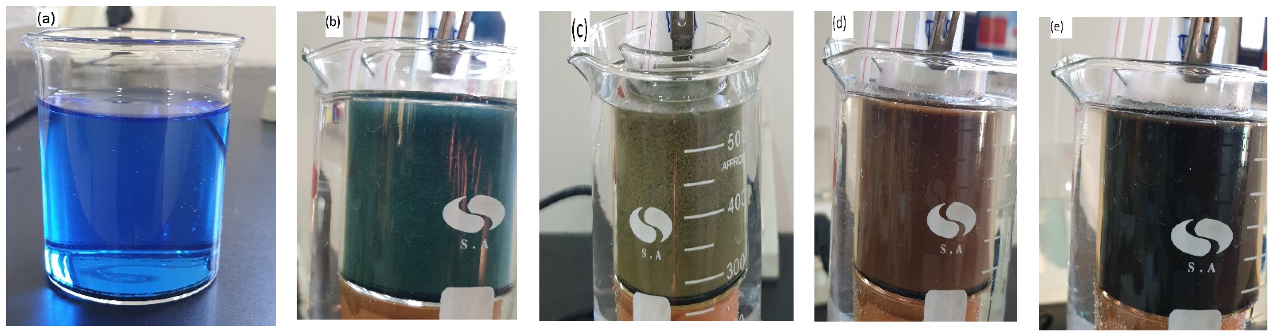
2.2. Deposition of Cu2S Thin Films

Initially, the CuSO4.5H2O precursor was used as a source of Cu+ ions by diluting the solution in 50 mL of distilled water. Under continuous stirring, 2 mL of triethanolamine (TEA; C6H15NO3) acted as a complex agent. Then, 15% of ammonia solution was consecutively added to achieve the desired pH value. Subsequently, the color of the solution changed to dark blue, which indicates the formation of copper ions. Then, 50 mL of thiourea (SC (NH2)2) solution as a source of S was added to the solution. The color of the solution changed from dark blue to dark brown during the deposition process, which indicates the steps of the formation of Cu2S thin films, as shown in Figure 1. The reactions inside the bath can be expressed as shown in Equations (1) and (2) [36]. Thereafter, the substrate was immersed vertically in the solution. The deposition process was carried out at various deposition parameters and presented in Table 1.
CuSO4.5H2O + n(TEA) ⟶ [Cu(TEA)n]2+ +SO4 +5H2O
[Cu(TEA)n]2+ +SC (NH2)2 +2OH ⟶ Cu2S + [NC_NH2] +2H2O
The thickness of Cu2S was measured using an optical interferometer technique [38,39,40]:
d = Δ x x   λ 2
where d is the thin film thickness, He–Ne is the laser wavelength (λ = 632.8 nm), ∆x is the distance between two fringes, and x is the width of the fringe.

2.3. Characterization of Cu2S Thin Films

The morphological properties of Cu2S thin films has been studied by the MIRA 3 TESCAN scanning electron microscopy (SEM). The optical transmission measurements of Cu2S thin films were obtained using an UV–Vis spectrophotometer (JANEWAY 6850) in the range of 350–1100 nm.
The direct energy bandgap of Cu2S thin films was calculated using Tauc’s equation:
( α h ν ) 2 = B ( h ν E g ) n
where the bandgap energy (Eg), the transmittance (T), the absorption (A), and the absorption coefficient (α) are given by (=2.303 log (T/d)). In addition, (hʋ) is the incident photon energy, n depends on the transition type (which is equal to 1/2 for the allowed direct transition and 2 for the indirect one), and (d) is the film thickness [41,42].

3. Results and Discussion

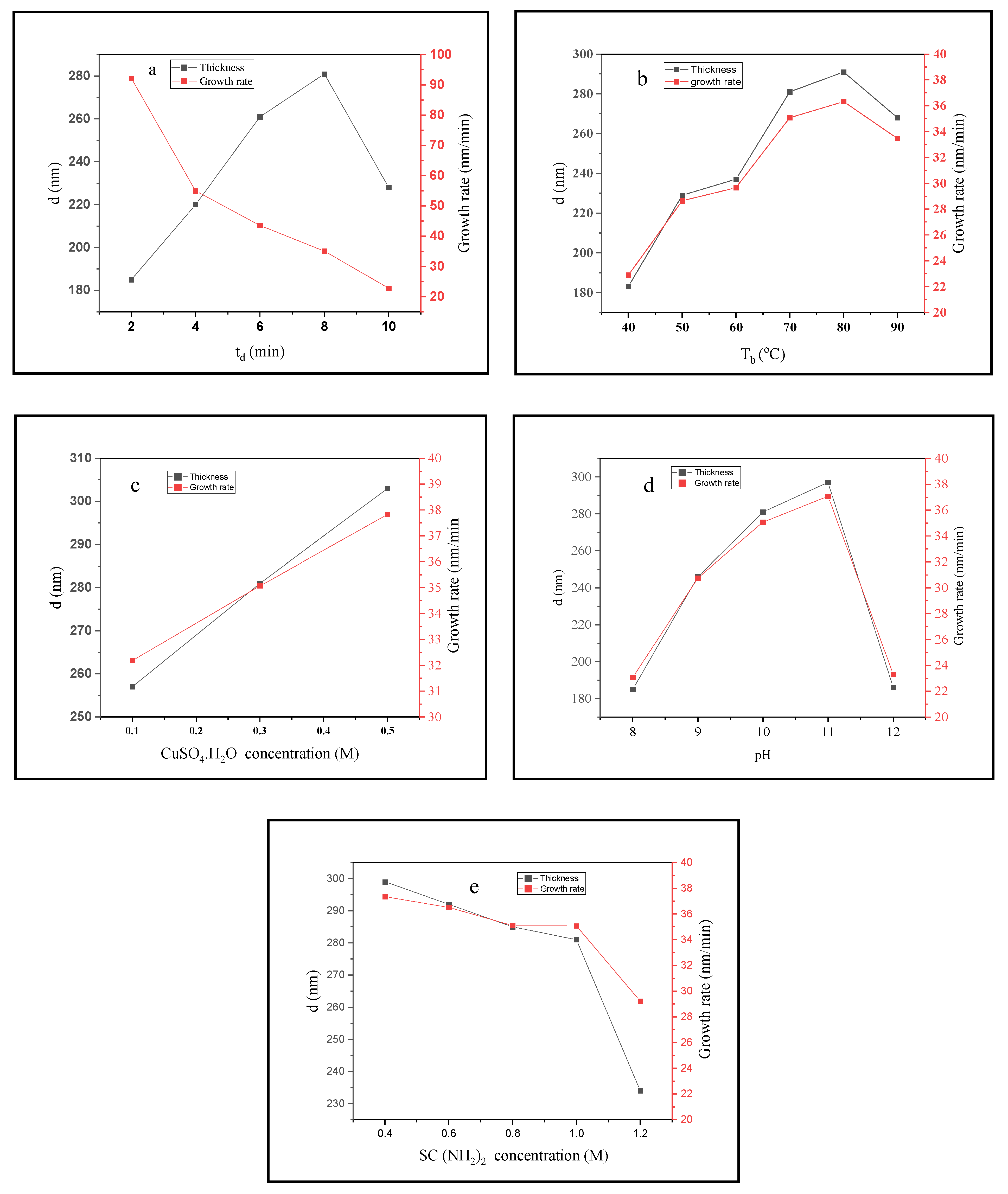
3.1. Deposition Parameters

Figure 2 presents the thickness and growth rate variation of Cu2S thin films as a function of deposition parameters (deposition time, bath temperature, CuSO4.5H2O concentration, pH value, and SC (NH2)2 concentration).
In Figure 2a, the thickness of deposited thin films increased almost linearly as deposition time increased from 2 to 6 min. Thereafter, the thickness started to decrease when the time reached 8 min, with a significant decrease at deposition time of 10 min. This decrement can be attributed to the porous formation of an outer layer and peeling off from the glass substrate [43]. The growth rate of deposited films (Figure 2a) gradually decreased with the deposition time, which can be attributed to the precursor consumption over time [42].
The thickness increased as bath temperature increased, until it reached its saturation point at a bath temperature of 70 °C. Thereafter, when the temperature reached 80 °C, the thickness started to decrease due to the desorption and/or dissolution of preformed Cu2S [44], as shown in Figure 2b. While the growth rate of deposited films gradually increased with the bath temperature due to additional generations of colloidal ions [42], as shown in Figure 2b.
In Figure 2c, the thickness and growth rate increased as CuSO4.5H2O concentration increased. This is attributed to the competition of heterogeneous nucleation on the substrate and homogeneous nucleation in the solution, which could modify the growth of thin films and increase the thickness [45].
The thickness of Cu2S thin films almost linearly increased from 185 to 297 nm as the pH value of bath solution increased from 8 to 11, as shown in Figure 2d.
This increase in thickness is attributed to the increment of OH- ions concentration in the solution that pushes the reaction of thiourea hydrolysis forward, causing the high generation of sulfide ions [46], as shown in Figure 2d. In addition, the growth rate increased as the pH value increased (Figure 2d).
Figure 2e shows the effect of SC (NH2)2 concentration on the thickness of deposited thin films.
Notably, the thickness of deposited thin films decreased as the SC (NH2)2 concentration increased due to the limited concentration of Cu2+ and S2 ions that was released in the solution [39]. The growth rate of Cu2S thin films can be seen in Figure 2e.

3.2. Physical Properties

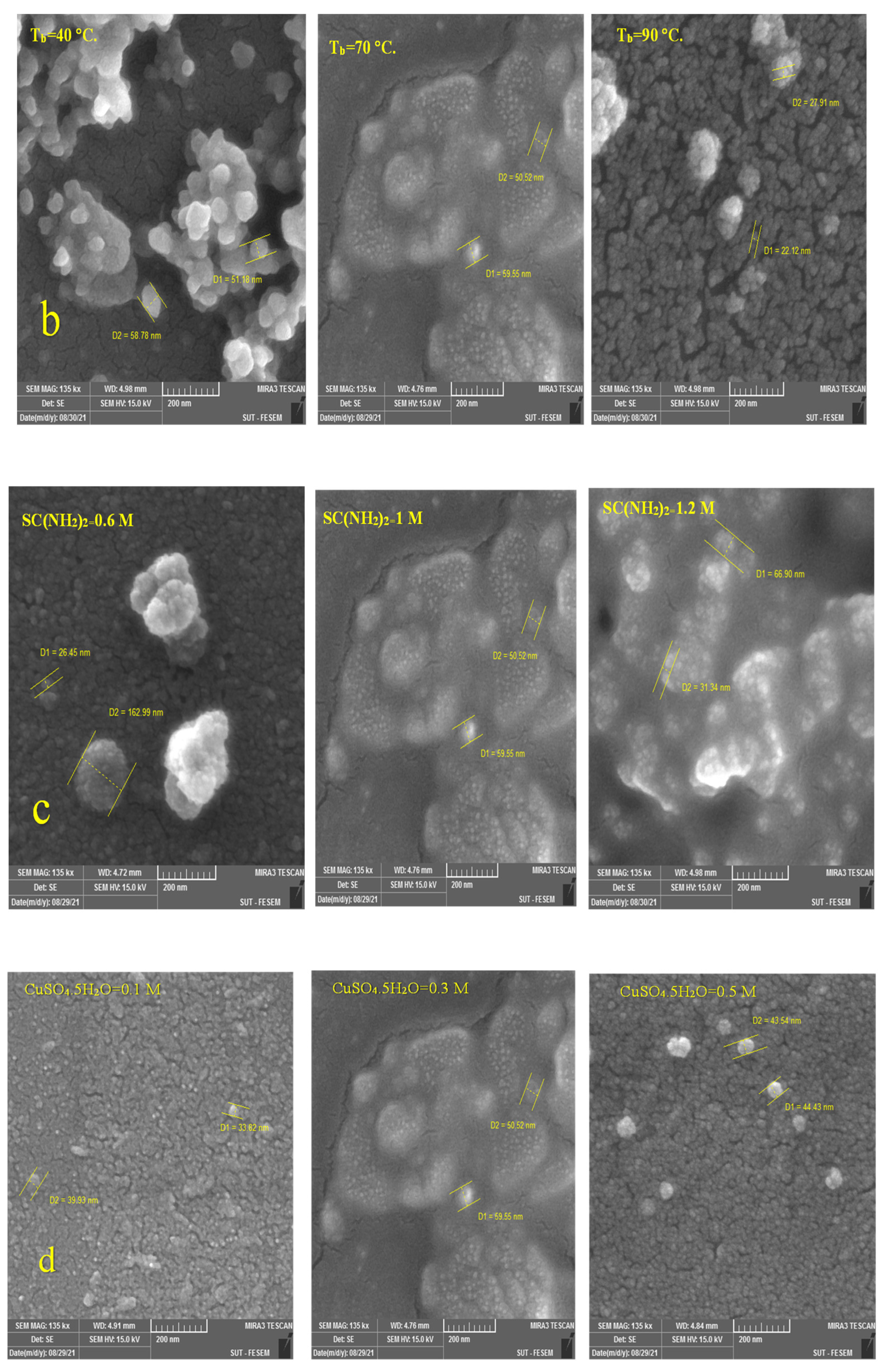
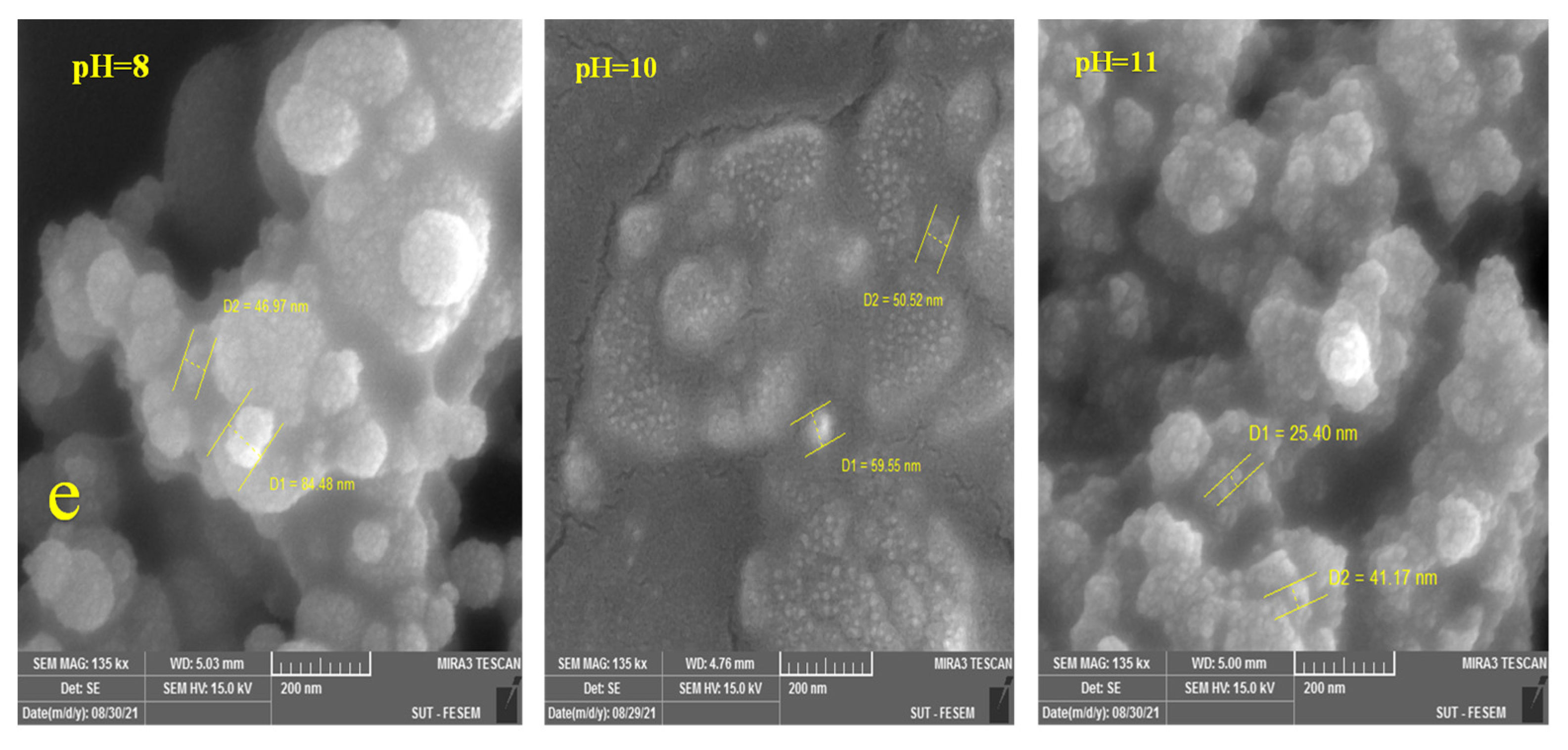
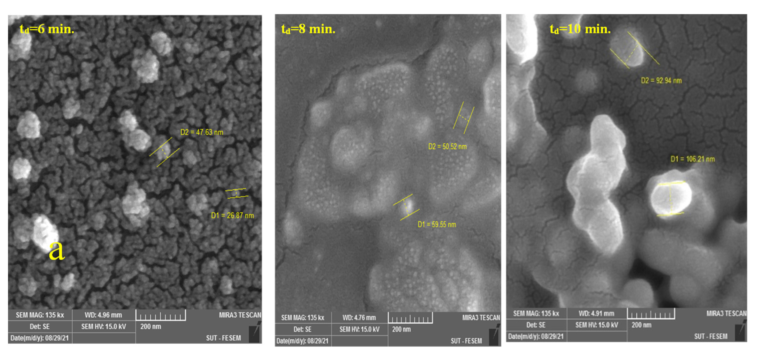
3.2.1. Morphological Properties

Figure 3 demonstrated the SEM images of Cu2S thin films at various deposition parameters (deposition time, bath temperature, pH value, CuSO4.5H2O concentration, and SC (NH2)2 concentration).
Figure 3a shows that the FESEM images of thin films at deposition time of 6 min were uniform, well covered, and homogenous without cracks. In addition, the increase in deposition time leads to the increase in aggregations. Moreover, few cracks were found in both deposited thin films at 8 and 10 min. The number and size of the grain increased from 37.25 to 99.57 nm as deposition time increased from 6 to 10 min. Figure 3a indicates that additional nucleation sites have formed [47]. The increase in bath temperature leads to the increase in compactness, homogeneity, and uniformity of films, as shown in Figure 3b. The surface of films deposited at 40 °C was not completely covered and had few cracks. However, the surface of films deposited at 70 and 90 °C was homogeneous, compact, and relatively completely covered and uniform.
The deposited films at 0.6 and 1 M of SC (NH2)2 concentration are well covered, uniform, and homogeneous with few small cracks on the surface deposited at 1 M of SC (NH2)2 concentration. The quality of thin films decreased as the SC (NH2)2 concentration increased to 1.2 M. Agglomerations and cracks existed on the film’s surface, as shown in Figure 3c. Deposited thin films at various CuSO4.5H2O molar concentrations were well covered, uniform, homogeneous, and few small cracks existed on the surface of the films deposited at 0.3 and 0.5 M, as shown in Figure 3d. However, the average particle sizes were 36.87, 55.03, and 43.98 nm for the deposited thin films at 0.1, 0.3, and 0.5 M of CuSO4.5H2O molar concentration, respectively. The increase in CuSO4.5H2O molar concentration leads to the increase in the number of clusters and agglomerated nanoparticles. The FESEM images of deposited films at different pH values are shown in Figure 3e. The films were homogeneous and well covered. However, the agglomerations and clusters increased as the pH value increased. The average particle sizes decreased from 65.72 to 33.28 nm as the pH value increased from 8 to 11. The increase in the pH value leads to noticeable changes in the morphology of deposited thin films due to the increment of OH ions. This leads the reaction forward, increase the attractive force and decrease repulsive force, which allow for the growth of oriented attachment (OA). When the particles are perfectly aligned, the common boundary is eliminated, resulting in the formation of larger well-defined morphology particles [48,49].

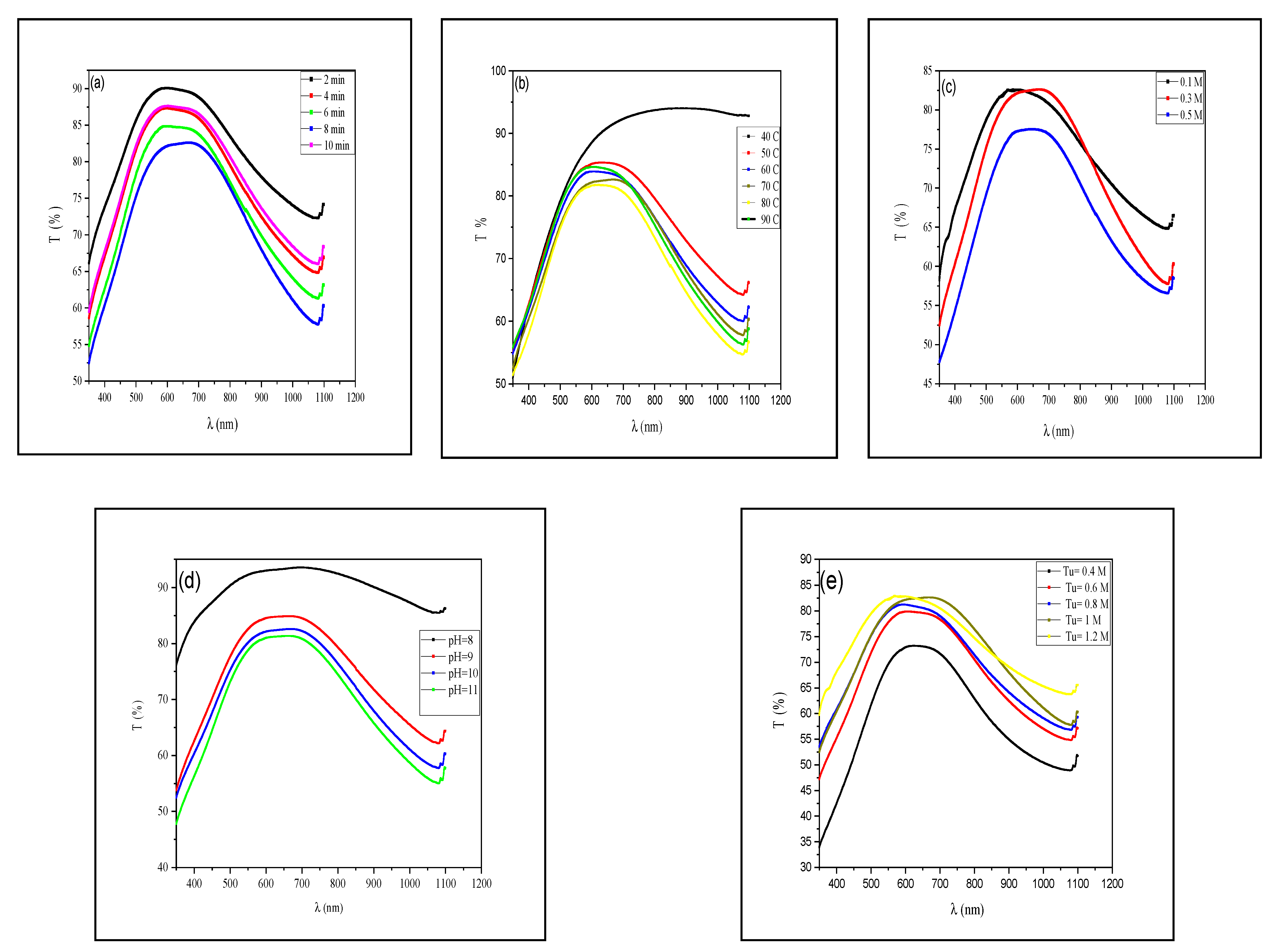
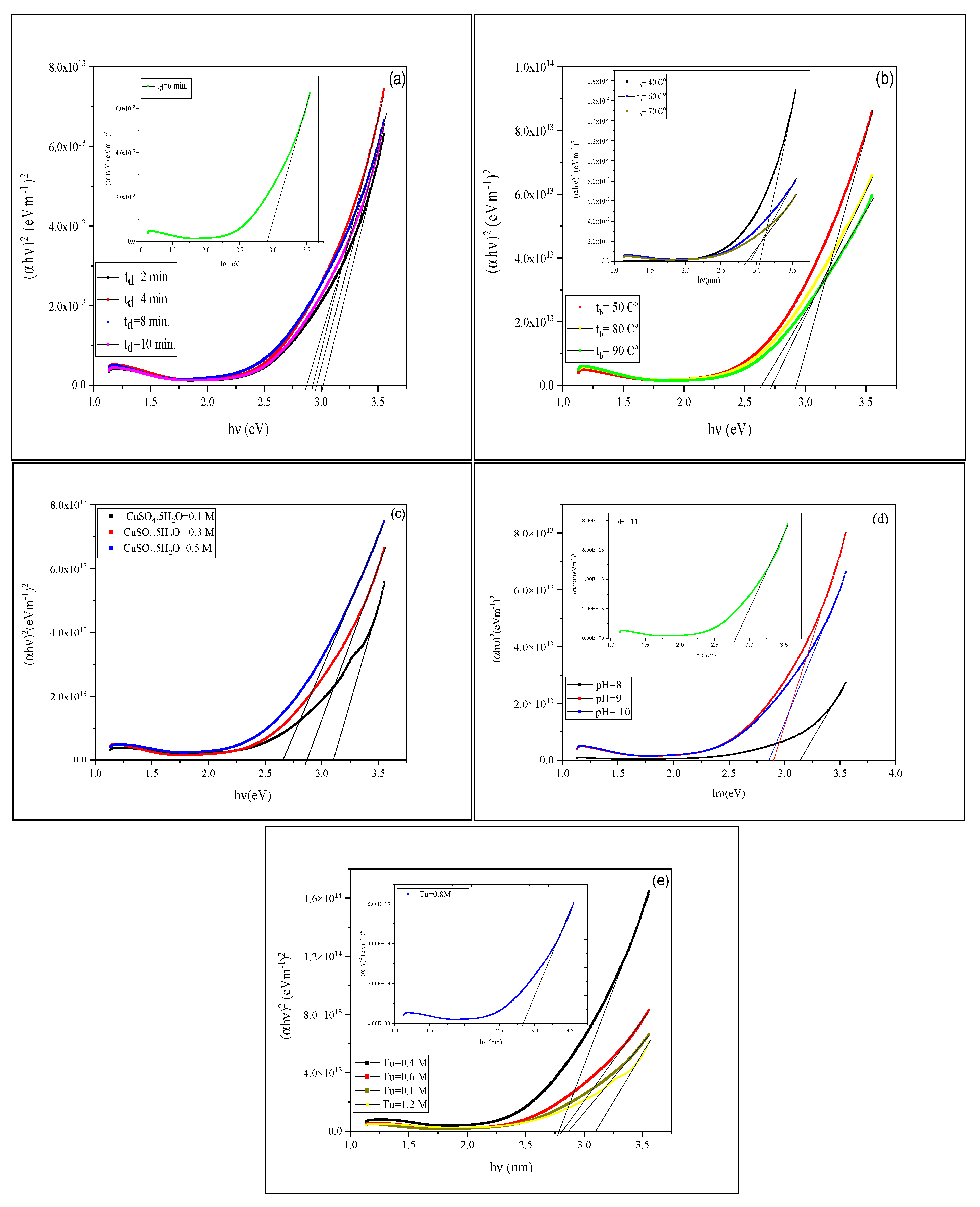
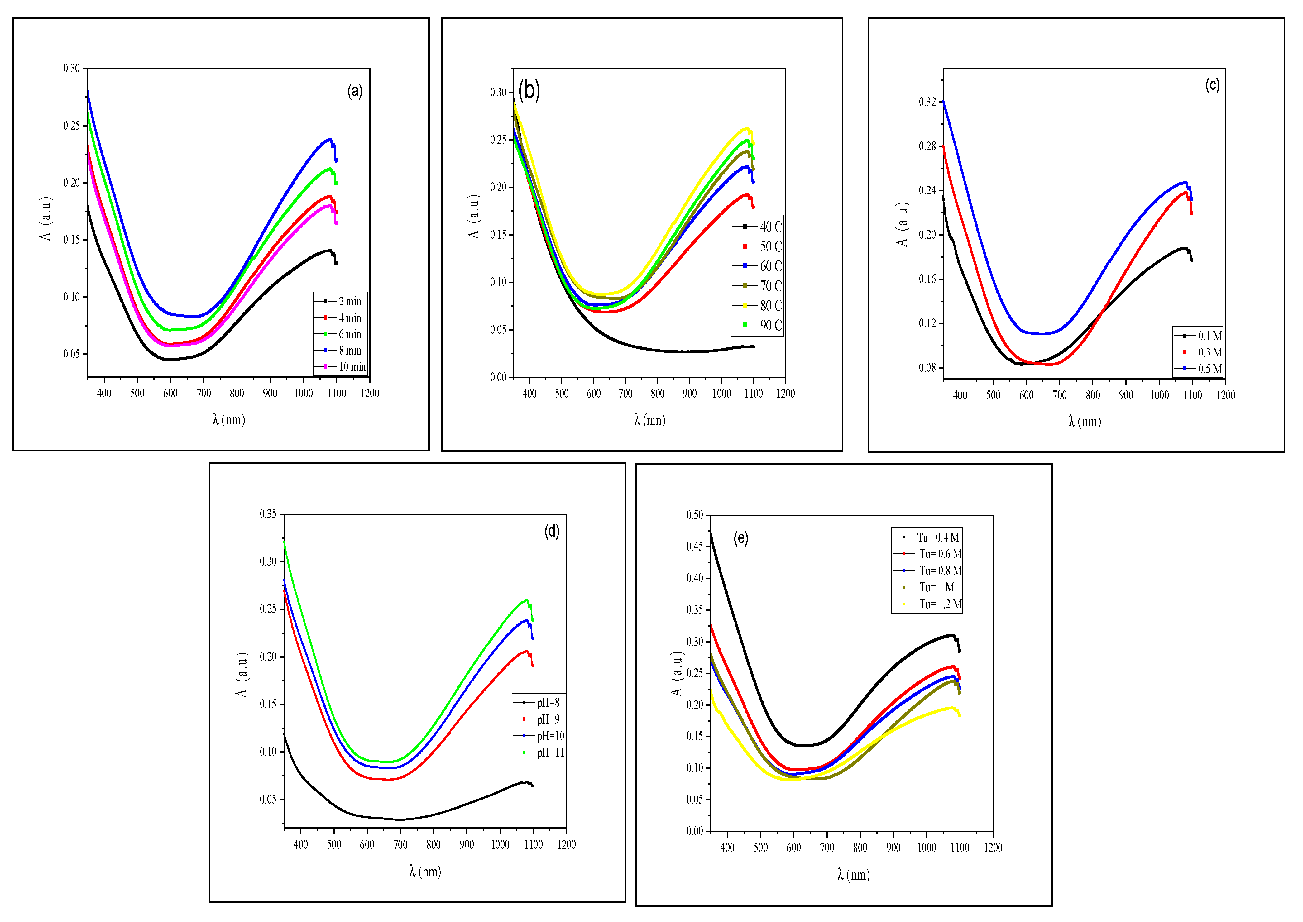
3.2.2. Optical Properties

Figure 4 shows the transmission of Cu2S thin films deposited at different deposition parameters (deposition time, bath temperature, CuSO4.5H2O concentration, SC (NH2)2 concentration, and pH value). Notably, the transmittance decreased as these parameters increased. However, the transmission increased as the SC (NH2)2 concentration increased. In addition, the transmittance of deposited thin films in the UV–Vis region rapidly increased until it reached its maximum peak at (λ = 600–650 nm). Thereafter, a slight decrease was found in the visible part before the rapid decrease in the NIR region, except for thin films deposited at (TB = 40 °C°) and (pH = 8), which have high transmittance of 94% and 86.2% at the NIR region. This decrease in transmission is due to the increase in the thickness of deposited Cu2S thin films [23].
Figure 5 shows the absorbance spectra of Cu2S thin films deposited at different deposition parameters. The absorbance of deposited thin films increased as deposition time, bath temperature, CuSO4.5H2O concentration, and pH value increased. In contrast, it decreased when the SC (NH2)2 concentration increased. In general, all of the deposited thin films have high absorbance at UV and NIR regions, except for thin films deposited at (Tb = 40 °C) and (pH = 8), which had low absorbance at the NIR region. In addition, thin films had low absorbance at the VIS region. Low transparency in UV region provides thin films with a coating quality for use in eyeglasses to protect the eye from UV radiation [23].
The high absorption coefficient indicates that deposited Cu2S thin films with various deposition parameters have a direct energy bandgap [19]. This was calculated from the extrapolation straight-line portion of the curve (αhυ)2 versus photon energy, as shown in Figure 6.
In Figure 6a and Table 2, the energy gap of deposited thin films decreased as deposition time increased due to the increase in thin films’ thickness [19] and crystallinity in the quantum size effect [43]. The decrease in energy gap with the increment of bath temperature is due to the increase in crystallite size, as shown in Figure 6b. This leads to the increased absorption and causes a shift in optical absorption edge towards longer wavelengths, and then the bandgap decreases [50]. In Figure 6c, the energy gap decreased linearly with the increase in CuSO4.5H2O concentration due to the increased grain size and low sulfur ions [24]. The obtained energy gap was slightly larger than the previous report by Ismail R.A. et al., which was prepared by a different precursor (CuCl2) [24]. The energy gap of thin films prepared at different pH values decreased as the pH value of bath solution increased due to the increase in thickness, as shown in Table 2. The obtained value is almost the same as the value obtained by Ahmed H.S. et al. [51], which was prepared by Cu2S thin films of a different precursor (CuCl2.2H2O). The effect of thickness on the energy gap could increase due to the height of crystalline films and large density of dislocation [21]. The energy gap increased as the SC (NH2)2 concentration increased due to the higher concentration of S- ions, which leads to a decrease in the thickness of thin films. The obtained values are slightly different from the obtained values by Muhammed A.M. et al. [52], which was prepared by Cu2S thin films of a different precursor (CuCl2).

4. Conclusions

Copper sulfide thin films were successfully deposited by the chemical bath deposition technique. The obtained results indicate that the thickness of deposited thin films strongly depends on the deposition parameters. It increased from 185 to 281 nm as deposition time increased, and from 183 to 291 nm as bath temperature increased. In addition, the thickness increased from 257 to 303 nm as the precursor concentration increased and from 185 to 297 nm as the pH value increased. However, the thickness decreased from 299 to 234 nm with the increasing thiourea concentration. The saturation was found only in the deposition time and bath temperature. The morphology of deposited thin films noticeably changed with the deposition times. The grains’ number and size increased with the deposition time. Moreover, the quality improved with the increasing deposition time and decreased at 10 min of deposition time. The deposited Cu2S thin films at various CuSO4.5H2O molar concentrations were compact, uniform, and homogeneous with different particle sizes and clusters, and the agglomerated nanoparticles increased as the CuSO4.5H2O molar concentration increased. Lower concentrations of thiourea provided compact and homogeneous thin films. The average particle sizes increased as the thiourea concentration increased. The morphology of deposited thin films improved and agglomerated nanoparticles increased as bath temperature increased. The morphology of deposited thin films remarkably changed with the pH value. Deposited thin films at higher pH values were covered almost completely with deposited nanoparticles. The optical measurements demonstrate that almost all of the deposited thin films have high transmission and low absorption in the visible region, while transmittance decreased and absorbance increased in the UV and NIR regions. The energy bandgap of thin films decreased with the increasing deposition time (3.01–2.95 eV), bath temperature (3.04–2.63 eV), CuSO4.5H2O concentration (3.1–2.6 eV), and pH value (3.14–2.75 eV), except for thiourea concentration, where it decreased with the increase in thiourea concentration (2.79–3.09 eV). Furthermore, all of the deposited thin films have high energy bandgaps and are slightly larger than those obtained by other works.

Author Contributions

Conceptualization, R.Y.M.; methodology, R.Y.M. and H.S.A.; software, H.S.A.; validation, R.Y.M. and H.S.A.; formal analysis, R.Y.M. and H.S.A.; investigation, R.Y.M. and H.S.A.; resources, R.Y.M.; data curation, R.Y.M. and H.S.A.; writing—original draft preparation, H.S.A.; writing—review and editing, R.Y.M.; visualization, R.Y.M. and H.S.A.; supervision, R.Y.M.; project administration, R.Y.M. All authors have read and agreed to the published version of the manuscript.

Funding

This research received no external funding.

Institutional Review Board Statement

Not applicable.

Informed Consent Statement

Not applicable.

Data Availability Statement

Not applicable.

Acknowledgments

The authors are thankful to the University of Duhok for their full support.

Conflicts of Interest

The authors declare no conflict of interest.

References

  1. Cruz, J.S.; Hernández, S.M.; Coronel, J. Characterization of CuxS thin films obtained by CBD technique at differents annealing temperatures. Chalcogenide Lett. 2012, 9, 85–91. [Google Scholar]
  2. Munce, C.G. Chemical Bath Deposition of Copper Sulfide Thin Films; Griffith University: Queensland, Australia, 2008. [Google Scholar]
  3. Sagade, A.; Sharma, R. Copper sulphide (CuxS) as an ammonia gas sensor working at room temperature. Sensors Actuators B Chem. 2008, 133, 135–143. [Google Scholar] [CrossRef]
  4. Adelifard, M.; Eshghi, H.; Mohagheghi, M.M.B. Comparative studies of spray pyrolysis deposited copper sulfide nanostructural thin films on glass and FTO coated glass. Bull. Mater. Sci. 2012, 35, 739–744. [Google Scholar] [CrossRef]
  5. More, P.; Dhanayat, S.; Gattu, K.; Mahajan, S.; Upadhye, D.; Sharma, R. Annealing effect on Cu2S thin films prepared by chemical bath deposition. In AIP Conference Proceedings; AIP Publishing LLC: Melville, NY, USA, 2016. [Google Scholar]
  6. Dhondge, A.D.; Gosavi, S.R.; Gosavi, N.M.; Sawant, C.P.; Patil, A.M.; Shelke, A.R.; Deshpande, N.G. Influence of Thickness on the Photosensing Properties of Chemically Synthesized Copper Sulfide Thin Films. World J. Condens. Matter Phys. 2015, 05, 1–9. [Google Scholar] [CrossRef] [Green Version]
  7. Sabah, F.A.; Ahmed, N.M.; Hassan, Z.; Rasheed, H.S. Effect of Annealing on the Electrical Properties of CuxS Thin Films. Procedia Chem. 2016, 19, 15–20. [Google Scholar] [CrossRef] [Green Version]
  8. Bharathi, B.; Thanikaikarasan, S.; Kollu, P.; Chandrasekar, P.V.; Sankaranarayanan, K.; Shajan, S. Effect of substrate on electroplated copper sulphide thin films. J. Mater. Sci. Mater. Electron. 2014, 25, 5338–5344. [Google Scholar] [CrossRef]
  9. Naji, I.; Sleman, U. Influence of precursor molar ratios on the physical properties of nanocrystalline Cu2−xS thin films prepared by chemical bath deposition method. Chalcogenide Lett. 2018, 15, 317–328. [Google Scholar]
  10. Wang, L.-W. High ChalcociteCu2S: A Solid-Liquid Hybrid Phase. Phys. Rev. Lett. 2012, 108, 085703. [Google Scholar] [CrossRef] [Green Version]
  11. Guo, Y.; Wu, Q.; Li, Y.; Lu, N.; Mao, K.; Bai, Y.; Zhao, J.; Wang, J.; Zeng, X.C. Copper (i) sulfide: A two-dimensional semiconductor with superior oxidation resistance and high carrier mobility. Nanoscale Horiz. 2019, 4, 223–230. [Google Scholar] [CrossRef]
  12. Hedlund, J.K.; Estrada, T.G.; Walker, A.V. Chemical Bath Deposition of Copper Sulfide on Functionalized SAMs: An Unusual Selectivity Mechanism. Langmuir 2020, 36, 3119–3126. [Google Scholar] [CrossRef]
  13. Patil, M.; Sharma, D.; Dive, A.; Mahajan, S.; Sharma, R. Synthesis and Characterization of Cu2S Thin Film Deposited by Chemical Bath Deposition Method. Procedia Manuf. 2018, 20, 505–508. [Google Scholar] [CrossRef]
  14. Yamamoto, T.; Kubota, E.; Taniguchi, A.; Dev, S.; Tanaka, K.; Osakada, K.; Sumita, M. Electrically conductive metal sulfide-polymer composites prepared by using organosols of metal sulfides. Chem. Mater. 1992, 4, 570–576. [Google Scholar] [CrossRef]
  15. Kassim, A.N.; Min, H.S.; Siang, L.K.; Nagalingam, S.A. SEM, EDAX and UV-Visible studies on the properties of Cu2S thin films. Chalcogenide Lett. 2011, 8, 405–410. [Google Scholar]
  16. Li, H.; Wang, Y.; Jiang, J.; Zhang, Y.; Peng, Y.; Zhao, J. CuS Microspheres as High-Performance Anode Material for Na-ion Batteries. Electrochimica Acta 2017, 247, 851–859. [Google Scholar] [CrossRef]
  17. Liu, Y.; Zhou, Z.; Zhang, S.; Luo, W.; Zhang, G. Controllable synthesis of CuS hollow microflowers hierarchical structures for asymmetric supercapacitors. Appl. Surf. Sci. 2018, 442, 711–719. [Google Scholar] [CrossRef]
  18. Guo, K.; Chen, X.; Han, J.; Liu, Z. Synthesis of ZnO/Cu2S core/shell nanorods and their enhanced photoelectric performance. J. Sol-Gel Sci. Technol. 2014, 72, 92–99. [Google Scholar] [CrossRef]
  19. Ismail, R.A.; Al-Samarai, A.-M.E.; Muhammed, A.M. High-performance nanostructured p-Cu2S/n-Si photodetector prepared by chemical bath deposition technique. J. Mater. Sci. Mater. Electron. 2019, 30, 11807–11818. [Google Scholar] [CrossRef]
  20. Zhan, Y.; Shao, Z.; Jiang, T.; Ye, J.; Wu, X.; Zhang, B.; Ding, K.; Wu, D.; Jie, J. Cation exchange synthesis of two-dimensional vertical Cu2S/CdS heterojunctions for photovoltaic device applications. J. Mater. Chem. A 2019, 8, 789–796. [Google Scholar] [CrossRef]
  21. Ramya, M.; Ganesan, S. Study of thickness dependent characterictics of Cu2S thin film for various applications. Iran. J. Mater. Sci. Eng. 2011, 8, 34–40. [Google Scholar]
  22. Podder, J.; Kobayashi, R.; Ichimura, M. Photochemical deposition of CuxS thin films from aqueous solutions. Thin Solid Films 2004, 472, 71–75. [Google Scholar] [CrossRef]
  23. Aniefuna, N.K.; Ezenwaka, L.; Umeokwonna, N. Effect of deposition time on the optical properties of Copper Sulphide thin films fabricated by chemical bath deposition method. In Proceedings of the 1st African International Conference/Workshop on Applications of Nanotechnology to Energy, Health and Environment, Enugu, Nigeria, 23–29 March 2014; pp. 275–279. [Google Scholar]
  24. Ismail, R.A.; Al-Samarai, A.E.; Ali, A.M.M. Effect of molar concentration of CuCl2 on the characteristics of Cu2S film. Opt. Quantum Electron. 2020, 52, 1–14. [Google Scholar] [CrossRef]
  25. He, Y.; Polity, A.; Österreicher, I.; Pfisterer, D.; Gregor, R.; Meyer, B.; Hardt, M. Hall effect and surface characterization of Cu2S and CuS films deposited by RF reactive sputtering. Phys. B Condens. Matter 2001, 308, 1069–1073. [Google Scholar] [CrossRef]
  26. Kosoljitkul, P.; Rakkroekkong, P.; Vas-Umnuay, P. Parameter-controllable microchannel reactor for enhanced deposition of copper sulfide thin films. Thin Solid Films 2018, 646, 150–157. [Google Scholar] [CrossRef]
  27. Su, Y.-W.; Paul, B.K.; Chang, C.-H. Investigation of CdS nanoparticles formation and deposition by the continuous flow microreactor. Appl. Surf. Sci. 2019, 472, 158–164. [Google Scholar] [CrossRef]
  28. Isac, L.A.; Duta, A.; Kriza, A.; Nanu, M.; Schoonman, J. Crystal order in Cu2S thin films obtained by spray pyrolysis. J. Optoelectron. Adv. Mater. 2007, 9, 1265–1268. [Google Scholar]
  29. Nho, P.V.; Ngan, P.H.; Tien, N.Q.; Viet, H.D. Preparation and characterization of low resistivity CuS films using spray pyrolysis. Chalcogenide Lett. 2012, 9, 397–402. [Google Scholar]
  30. Zhuge, F.; Li, X.; Gao, X.; Gan, X.; Zhou, F. Synthesis of stable amorphous Cu2S thin film by successive ion layer adsorption and reaction method. Mater. Lett. 2009, 63, 652–654. [Google Scholar] [CrossRef]
  31. Pathan, H.; Desai, J.; Lokhande, C. Modified chemical deposition and physico-chemical properties of copper sulphide (Cu2S) thin films. Appl. Surf. Sci. 2002, 202, 47–56. [Google Scholar] [CrossRef]
  32. Omwoyo, J.G. Characterization of Cu2S/SnO2: F pn Junction for Solar CEll Applications; Kenyatta University: Nairobi, Kenya, 2019. [Google Scholar]
  33. Gashaw Hone, F.; Abza, T. Short Review of Factors Affecting Chemical Bath Deposition Method for Metal Chalcogenide Thin Films. Int. J. Thin Film. Sci. Technol. 2019, 8, 3. [Google Scholar]
  34. Allouche, N.K.; Ben Nasr, T.; Guasch, C.; Turki, N.K. Optimization of the synthesis and characterizations of chemical bath deposited Cu2S thin films. Comptes Rendus. Chim. 2010, 13, 1364–1369. [Google Scholar] [CrossRef]
  35. Hone, F.G.; Dejene, F.B. Cationic concentration and pH effect on the structural, morphological and optical band gap of chemically synthesized lead sulfide thin films. J. Mater. Res. Technol. 2019, 8, 467–474. [Google Scholar] [CrossRef]
  36. Kırmızıgül, F.; Güneri, E.; Gümüş, C. Effects of different deposition conditions on the properties of Cu2S thin films. Philos. Mag. 2013, 93, 511–523. [Google Scholar] [CrossRef]
  37. Patil, M.; Sharma, D.; Dive, A.; Mahajan, S.; Sharma, R. Study of various synthesis techniques of nanomaterials. In AIP Conference Proceedings; AIP Publishing LLC: Melville, NY, USA, 2018. [Google Scholar]
  38. Chopra, K.L. Thin Film Phenomena; McGraw-Hill: New York, NY, USA, 1969. [Google Scholar]
  39. Khalil, M.H.; Mohammed, R.Y.; Ibrahem, M.A. The Influence of CBD Parameters on the Energy Gap of ZnS Narcissus-Like Nanostructured Thin Films. Coatings 2021, 11, 1131. [Google Scholar] [CrossRef]
  40. Makuła, P.; Pacia, M.; Macyk, W. Investigation of optical properties of the PbS/CdS thin films by thermal Evaporation. J. Electron Devices 2012, 12, 761–766. [Google Scholar]
  41. Makuła, P.; Pacia, M.; Macyk, W. How to Correctly Determine the Band Gap Energy of Modified Semiconductor Photocatalysts Based on UV–Vis Spectra; ACS Publications: Washington, DC, USA, 2018. [Google Scholar]
  42. Mohammed, K.A.; Ahmed, S.M.; Mohammed, R.Y.; Mohammed, K. Investigation of Structure, Optical, and Electrical Properties of CuS Thin Films by CBD Technique. Crystals 2020, 10, 684. [Google Scholar] [CrossRef]
  43. Shinde, M.S.; Ahirrao, P.B.; Patil, I.J.; Patil, R.S. Thickness Dependent Electrical and Optical Properties of Nanocrystalline Copper Sulphide Thin Films Grown by Simple Chemical Route; NISCAIR-CSIR: New Delhi, India, 2012. [Google Scholar]
  44. Ouachtari, F.; Rmili, A.; Elidrissi, B.; Bouaoud, A.; Erguig, H.; Elies, P. Influence of Bath Temperature, Deposition Time and S/Cd Ratio on the Structure, Surface Morphology, Chemical Composition and Optical Properties of CdS Thin Films Elaborated by Chemical Bath Deposition. J. Mod. Phys. 2011, 02, 1073–1082. [Google Scholar] [CrossRef] [Green Version]
  45. Sangamesha, M.; Pushapalatha, K.; Shekar, G. Effect of concentration on structural and optical properties of CuS thin films. Int. J. Pure Appl. Res. Eng. Technol. 2013, 2, 227. [Google Scholar]
  46. Vas-Umnuay, P.; Chang, C.-H. Growth Kinetics of Copper Sulfide Thin Films by Chemical Bath Deposition. ECS J. Solid State Sci. Technol. 2013, 2, P120–P129. [Google Scholar] [CrossRef]
  47. Manjulavalli, T.; Kannan, A. Effects of deposition time on structural, optical and electrical properties of chemically deposited Cu2S thin films. J. Chem. Tech. Res. 2015, 8, 607–616. [Google Scholar]
  48. Xu, H.; Dong, J.; Chen, C. One-step chemical bath deposition and photocatalytic activity of Cu2O thin films with orientation and size controlled by a chelating agent. Mater. Chem. Phys. 2014, 143, 713–719. [Google Scholar] [CrossRef]
  49. Yu, M.; Draskovic, T.I.; Wu, Y. Understanding the crystallization mechanism of delafossite CuGaO2 for controlled hydrothermal synthesis of nanoparticles and nanoplates. Inorg. Chem. 2014, 53, 5845–5851. [Google Scholar] [CrossRef] [PubMed]
  50. Rondiya, S.; Rokade, A.; Gabhale, B.; Pandharkar, S.; Chaudhari, M.; Date, A.; Chaudhary, M.; Pathan, H.; Jadkar, S. Effect of Bath Temperature on Optical and Morphology Properties of CdS Thin Films Grown by Chemical Bath Deposition. Energy Procedia 2017, 110, 202–209. [Google Scholar] [CrossRef]
  51. Ahmed, H.S.; Mohammed, R.Y.; Khalil, M.H. Effects of Deposition Time And PH on The Characterization of Chemically Synthesized Composite Nano-Wires of Cu2S Thin Films. Sci. J. Univ. Zakho 2021, 9, 184–192. [Google Scholar] [CrossRef]
  52. Muhammed, A.M.; Ibrahim, A.E.; Ismail, R.A. Study an Effect of Thiourea Concentration on the Structural, Optical and Electrical Properties of (Cu2S) film Prepared by Chemical Bath Deposition (CBD). Kirkuk Univ. J.-Sci. Stud. 2019, 14, 97–115. [Google Scholar] [CrossRef]
Figure 1. The stages of chemical bath deposition of Cu2S: (a) 0 min, (b) after 2 min, (c) 3 min, (d) 5 min, and (e) 6.5 min with CuSO4.5H2O = 3 M, SC (NH2)2 = 1 M, bath temperature = 70 °C, and pH = 10.
Photonics 09 00161 g001
Figure 2. The thickness and growth rate variation of Cu2S thin films as a function of deposition parameters: (a) Deposition time, (b) bath temperature, (c) CuSO4.5H2O concentration, (d) pH value, (e) and SC (NH2)2 concentration.
Photonics 09 00161 g002
Figure 3. FESEM images of Cu2S thin films at different deposition parameters: (a) Deposition time (td), (b) bath temperature (Tb), (c) SC (NH2)2 concentration, (d) CuSO4.5H2O concentration, and (e) pH value.
Photonics 09 00161 g003aPhotonics 09 00161 g003bPhotonics 09 00161 g003c
Figure 4. Transmission spectrums of Cu2S thin films as a function of different deposition parameters: (a) Deposition time, (b) bath temperature, (c) CuSO4.5H2O concentration, (d) pH value, and (e) SC (NH2)2 concentration.
Photonics 09 00161 g004
Figure 5. Absorbance of Cu2S thin films as a function of different deposition parameters: (a) Deposition time, (b) bath temperature, (c) CuSO4.5H2O concentration, (d) pH value, and (e) SC (NH2)2 concentration.
Photonics 09 00161 g005
Figure 6. Variation of (αhʋ)2 with (hʋ) with deposition parameters): (a) Deposition time, (b) bath temperature, (c) CuSO4.5H2O concentration, (d) pH value, and (e) SC (NH2)2 concentration.
Photonics 09 00161 g006
Table 1. Chemical bath solutions.
Bath No.t (min)CuSO4.5H2O (M)SC (NH2)2 (M)T (°C)pH ValueTEA (mL)
12–10 step 20.3170102
280.1, 0.5170102
380.30.4–1.2 step 0.270102
480.31708, 9, and 112
580.3140, 50, 60, 80, and 90102
Table 2. Bandgap variation with different deposition parameters.
Bath No.123456
Deposition time (min)246810-
Eg (eV)3.012.922.92.862.95-
Bath temprature (°C)405060708090
Eg (eV)3.042.922.92.862.722.63
CuSO4.5H2O concentration (M)0.10.30.5---
Eg (eV)3.12.862.65
pH Value891011--
Eg (eV)3.142.92.862.75
SC (NH2)2 concentration (M)0.40.60.811.2-
Eg (eV)2.792.812.832.863.09-
Publisher’s Note: MDPI stays neutral with regard to jurisdictional claims in published maps and institutional affiliations.

