Abstract
The discussion of resonance mechanisms for artificial structural units has always been a key to producing highly efficient, active and tunable meta-devices in the fields of controlling surface plasmon polaritons (SPPs) to generate surface plasmonic bending beams (SPBs). In this study, an array of 20 antisymmetric double V-shaped structures was designed to generate an SPB. The arms of the double V-shaped structures were panned to control the electric field intensity distributions of the SPB. The influence of the polarization states (such as polarization angles, linearly polarized (LP), left-circularly polarized (LCP) and right-circularly polarized (RCP) light) of the incident light on electric field intensity of SPB is discussed. These results can be well explained by the theory of dipole radiation. The numerical simulation results are in good agreement with the theoretical analysis. It is hoped that these results will help guide subsequent work in optimizing SPB generators.
1. Introduction
Surface plasmon polaritons (SPPs), special two-dimensional (2D) electromagnetic waves that propagate along a metal–dielectric interface, have attracted much attention in recent years [1,2,3]. Surface plasmonic bending beams (SPBs) are obtained by artificial controlling SPPs, allowing them to propagate along the designed curved paths while maintaining their shapes, with potential applications in photon manipulation, optical trapping [4,5,6,7], optical communication and optical computation [8,9]. In recent years, new physical materials and models have been introduced to potentially improve studies on the regulation of SPBs. For example, similar to conventional optical devices, the propagation phase was utilized to control SPPs and generate an SPB [10,11,12,13,14]. Considering their refractive index and Bragg scattering, various structures, such as nano-bump, holes, gaps and grooves, were designed to realize SPBs by controlling SPP wavefronts. These SPBs include the Airy beam [15], Bessel beam [16], Weber beam [17], Mathieu beam [18], cosine-Gauss beam [19], plasmonic arbitrary bending beams [20,21], focused SPPs [22], switchable SPPs [23] and spiral SPPs [24]. More complex control of SPPs may be realized by utilizing the freedom to flexibly and creatively arrange nanostructures as desired. However, due to the need to rely on multiple scattering effects, the size of these devices is required to be on the order of several wavelengths.
Metasurfaces, 2D artificial structures made of subwavelength metallic or dielectric materials, have been widely used for wavefront reshaping. Compared with the traditional 3D metamaterials, they can exploit new degrees of freedom to manipulate optical fields [25]. Various physical effects, including anomalous reflections or deflections, focused electromagnetic waves [26], the photonic spin Hall effect [27] and excitation of SPBs, such as Bessel beams, Airy beams and vortex beams, were realized by designing various metasurfaces [28,29]. In particular, developments of multiplexing and multifunctional metasurfaces have enabled concurrent tasks through dramatically compact designs [30]. However, the working efficiency was particularly low when using a single layer of metasurface structures [31]. Hence, multi-layer metasurface structures, such as reflective and transmission-mode Pancharatnam–Berry (PB) metasurfaces [32,33], were designed to improve the working efficiency by exhibiting both electric and magnetic responses that satisfy certain designed criteria [34]. Thus, highly efficient, active PB meta-devices that can actively tune and manipulate SPPs at fast switching speeds are a hot topic in metasurface research, though the PB and resonance mechanisms, especially internal interaction of resonance mechanisms between structure units, have always been key areas of interest.
Researchers have also achieved excellent results in improving the efficiency of excitation and effective propagation length of SPPs with the aim of expanding their potential practical applications. For example, parabola-shaped grooves were designed to generate focused SPPs of high-efficiency reflection and large effective propagation length [35,36,37]. The constructed gradient meta-coupler was proposed to achieve SPP excitation and wavefront tailoring simultaneously in the THz regime [38]. Likewise, straightforward design principles for metasurfaces, such as using metaholograms or metalenses, were proposed to achieve the highly efficient quarter-wave plate functionality by utilizing both co-polarized and cross polarized spin light [39]. Two broadband reflective PB metasurfaces were designed in tandem to realize high-efficiency photonic spin Hall effects and focusing of light [40]. In our previous investigation, to improve the efficiency of excitation of SPPs, the influence of the number of nanoslits in a structure on the resulting SPB was investigated. The results showed that the electric field intensity of the SPB exhibits a clear disturbance with the increase in the number of nanoslits [41]. In this study, an array of 20 antisymmetric double V-shaped structures was designed to generate an SPB. The influence of the structural parameters on the electric field intensity of the SPB was assessed by panning the arms of the double V-shaped structures. The results show that the electric field intensity of the SPB changes in a sine function distribution with the separation of the structural arms inside the double V-shaped structure. It was found that the electric field intensity of SPB is controlled by the polarization angle of the incident light, especially the by the left-circularly polarized (LCP) and right-circularly polarized (RCP) light, the mechanisms of which are also discussed. These results can be well explained by the theory of dipole radiation and will hopefully be useful for further design and optimization of SPB generators.
2. Theoretical Analysis and Structure
The SPB, a special beam of SPP waves, propagates in the 2D plane and satisfies the 2D Helmholtz equation, [18,22],
where is the wave vector of the SPP propagating in the plane and represents the distributions of the SPP waves in the x–y plane.
To understand the principle of generating SPBs, we restate the fundamental equations of electromagnetic wave radiation from electric dipole (ED) resonances in free space. If the current on the line element is expressed as , according to Maxwell’s equations, the electric and magnetic fields generated by ED are respectively expressed as
where E is the electric field, H is the magnetic field, is the angular frequency of the ED, r is the distance from the dipole, and and are the polar and azimuthal angles in spherical coordinate system, shown in Figure 1. Using the far-field approximation, (), and with the relationships, , and , Equation (2) can be simplified as:
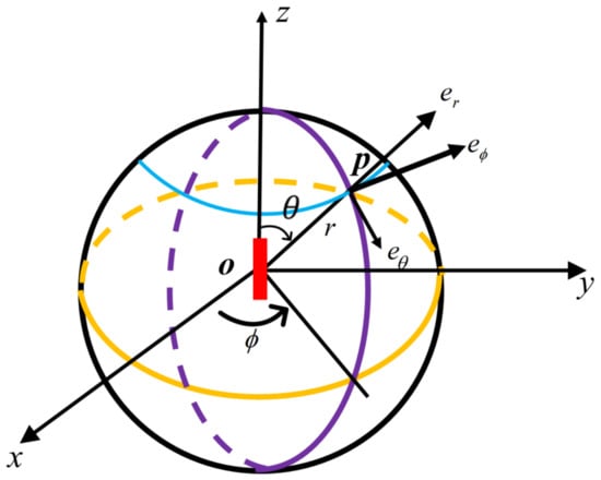
Figure 1.
Diagram of radiation of electric dipole.
The averaged Poynting vector of the far-field is,
According to the duality principle, the electric and magnetic fields of a MD can be directly obtained from Equation (3):
where S is the area of small electric current loop. Moreover, it should be noted that the E-plane pattern of MD is the same as H-plane pattern of ED, and the H-plane pattern of MD is same as E-plane pattern of ED.
We consider N electric dipoles evenly arranged along the x-direction with a uniform spacing, d, and unit amplitude. If the interaction between adjacent EDs is not considered, the electric field induced by the ED array can be expressed as
where is the phase difference between adjacent dipoles, respectively. is phase difference between two adjacent radiation sources, which is constant. Clearly, the radiation electric distributions of the ED array depend on the angles and . The function , as a directional factor, is related to the structure and orientation of the current element. In addition, the factor is related to the arrangement, amplitude and phase of the current element array. That is to say, various arrangements of current elements can be designed to generate special electromagnetic field intensities, which can be controlled by structure and orientation.
The above discussion only relates to a single dipole radiation source in free space. Obviously, we can apply this dipole radiation superposition principle to analyze the SPP wave radiation superposition in two-dimensional space. If multiple-like dipoles are used as the radiation sources—e.g., the antisymmetric double V-shaped structure in the inset of Figure 2—the electric field intensity of the SPP waves at a fixed point can been expressed as [42],
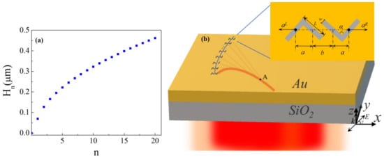
Figure 2.
(a) The calculated distances Hn of the n-th radiation source, (b) configuration of antisymmetric double V-shaped nanoslit structure.
Here, is the angle between the structure arm and the vertical direction (here, is fixed at 90°); and represent the real and imaginary parts of propagation constant of SPPs, respectively; and c is distance of the rightmost arm to the superposition of arbitrarily point A, which is constant. By simplifying, Equation (7) can be re-expressed as
The far-field distribution of the SPP waves from N independent radiation sources can be obtained as a superposition of the electric fields radiated from every source, , which can be expressed approximately as
To further discuss the effect of the polarization angle of incident light on the SPB, Equation (9) can be expressed approximately as
where γ is the polarization angle of the incident light. When we consider circularly polarized light, Equation (10) can be expressed approximately as
That is, the electric field intensity of the SPB can also be controlled by changing the polarization angle of incident light and polarization state (LCP/RCP) of light.
In this study, to generate the SPB, the phase modulation method was utilized [18]. The phase φ of the required SPB was calculated using Legendre transformation [17,18,19,20,21,22]. Here, for simplicity, the case of paraxial was applied. Thus, the phase of the required SPBs was obtained for paraxial regimes [18,19] , where , and is the first-order derivative of the designed bending trajectory f(y), for which the quadratic curve is chosen, where the constant, a, is 1.13 × 10⁻². The desired phase, is obtained to directly locate the position of every source. The distances are calculated when the number of each source is equal to 20, as shown in Figure 2a. The configuration of an Au/SiO2 structure used to generate the SPB is shown in Figure 2b. The thickness of the Au film and SiO2 substrate are fixed at 0.2 and 0.25 μm, respectively. The antisymmetric double V-shaped nanoslit arrays were designed on the Au film. The inset is a single antisymmetric double V-shaped nanoslit in a red wireframe. The arm length, L, and width, w, are set as 0.3 and 0.07 μm, respectively, and the angle between two adjacent nanoslits is set to 90°. In addition, a and b represent the horizontal distance between two arms of the V-shaped structure and between the adjacent arms of the two V-structures, respectively, and and represent the horizontal outward moving distance of leftmost arm and rightmost arms. The propagation properties of the SPPs were simulated using the finite-difference time-domain (FDTD) method using Ansys/Lumerical FDTD solutions software, a simulator within Lumerical’s device multiphysics simulation suite. The perfect matching layer (PML) boundary condition was applied, and the min mesh step is about μm. A plane wave of 0.8 μm was incident along z-direction into the V-shaped nanoslit array. The relative permittivity, εm, of the Au film was −24 + 1.506i at 0.8 μm [43]. The etch material (refractive index n = 1) in the software material database was selected as the material of V-shaped nanoslits.
3. Results and Discussion
The electric field intensity distribution in the x–y plane is depicted in Figure 3a, with polarization angle of incident light , b = 0.6 μm and μm. The black solid curve depicts the target quadratic curve, . It shows that the target SPB was generated and propagated along the desired trajectory. Figure 3b,c show the x- and y-components of the electric field of the generated parabolic beam, respectively. The electric field of the generated SPB was primarily x-polarized. The electric field intensity at point A (x = 20 μm, y = −10 μm) was about 0.65 times the intensity of the incident light wave, of magnitude 1 V/m.
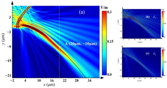
Figure 3.
Electric field intensity distribution in the polarization angle , b = 0.6 μm, and μm; (a) electric field norm, (b) electric field x component and (c) electric field y component.
To further understand the relationship between the electric field intensity of the SPB and the structural parameters, the electric field intensity distributions with different b in the x–y plane are depicted in Figure 4. The electric field intensity distributions with b = 0.3, 0.6, 0.9 and 1.2 μm are depicted in Figure 4a–d, respectively. The transverse electric field intensity distributions at x = 20 μm are depicted for different widths of b (from b = 0.3 to 1.2 μm, with step of 0.1 μm) in Figure 4e,f. Point A was selected to study the electric field intensity values for the different widths, b, shown in Figure 4g. The results reveal that as b increased from 0 to 0.3 μm, the electric field intensity of the SPB increased, yet decreasing as b increased from 0.3 to 0.6 μm, rising again as b increased from 0.6 to 0.9 μm. An equation was derived to fit the oscillatory result, which was , with a fitting quality coefficient R-square of 0.94. Thus, the relationship between the electric field intensity of the SPB and the width, b, being a sine distribution, is consistent with Equation (10).
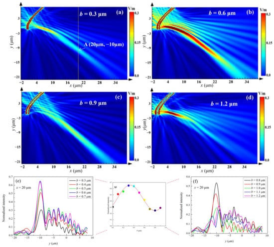
Figure 4.
(a–d) Electric field intensity distribution for b = 0.3, 0.6, 0.9 and 1.2 μm, respectively. (e,f) Transverse electric field intensity distribution at x = 20 μm for different widths of b. (g) Fitting diagram for electric field intensities at point A with varied widths of b.
Further studying the influence of structural parameters on the SPB, the leftmost arm of the antisymmetric double V-shaped structure was moved towards left and right. The transverse electric field intensity distributions at x = 20 μm with different and values in the x–y plane are depicted in Figure 5a–d with = 0°, a = 0.16 μm and b = 0.6 μm. Figure 5b,d show the electric field intensity values at point A for various values of and , respectively. The results show that the electric field intensity of the SPB increases for between 0 and 0.3 μm then decreases between 0.3 and 0.6 μm and increases again between 0.6 and 0.9 μm, satisfying the periodic distribution of sine. Similarly, the electric field intensity of SPB decreases for , between 0 and 0.4 μm, then increases between 0.4 and 0.8 μm and decreases again between 0.8 and 1.1 μm, also satisfying the periodic distribution of sine. The data were fitted using sine function distribution, with R-square values of 0.92 and 0.96 for and , respectively. Furthermore, the geometrical parameters such as L and w of the arms of the V-shaped structures greatly impact the electric field intensity of SPB, as does the angle between adjacent arms. The parameters in our structure were set as a result of optimization—when the angle between the arms is 90°, the maximum electric field intensity occurs for about L = 0.3 μm and w = 0.07 μm. The resulting the ratio of coupling coefficients of the SPPs with x- and y-polarization is about equal to 1 [41].
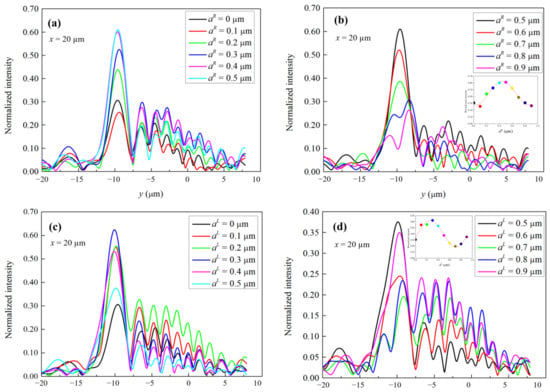
Figure 5.
Transverse electric field intensity distributions at x = 20 μm with different (a,b) and (c,d) in the x–y plane. The insets in (b,d) are electric field intensity values at point A for various values.
In addition, the relation between the electric field intensity and of an incident light was investigated using the structural parameters: a = 0.16 μm, b = 0.6 μm and μm. The polar plots of the electric field intensity at point A for various values of are shown in Figure 6a, which also shows a sine distribution. The equation to fit these data is given by , with an R-square of 0.95. This result demonstrates that the electric field intensity of SPB is controlled by the polarization angle of incident light and is consistent with the equation in our previous work [41]. The above incident light was linearly polarized (LP) light. Figure 6b shows the transverse electric field intensity at x = 20 μm under LCP and RCP light, which is contrasted with that for LP light at the same point shown in red. Here, we observe that the electric field intensity with LCP is stronger than that with LP and RCP. This agrees well with Equation (11).
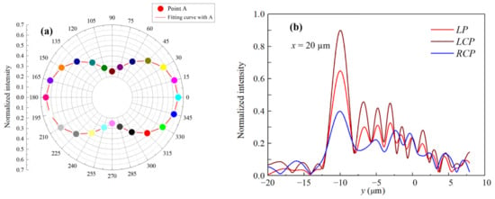
Figure 6.
(a) Polar diagram for electric field intensities at points A with varied polarization angle with a = 0.16 μm, b = 0.6 μm. (b) Transverse electric field intensity distribution at x = 20 μm for RCP/LCP/LP.
4. Conclusions
In summary, an array of 20 antisymmetric double V-shaped structures was designed to generate an SPB. The electric field intensity distributions of the SPB could be controlled by panning the arms of the structures and changing polarization angle of the incident light. Moreover, the relationship between the electric field intensity of SPB and structures, the polarization angle of incident light, satisfies the sine distribution as understood from electric dipole radiation theory. In addition, the electric field intensity values could be controlled differently by RCP, LCP and LP incident light. The generated SPB can be used to perform optical communication and optical computation. These results will hopefully be useful for the design and optimization of SPB generators.
Author Contributions
Conceptualization, X.L. (Xiaoming Li) and H.L.; methodology, X.L. (Xiaoming Li) and H.L.; software, L.W.; validation, X.L. (Xiaoming Li), H.Z. and X.L. (Xueli Li); formal analysis, X.L.; investigation, X.L. (Xueli Li); resources, H.Z.; data curation, X.L. (Xiaoming Li); writing—original draft preparation, X.L. (Xiaoming Li); writing—review and editing, X.L. (Xiaoming Li); visualization, L.W.; supervision, X.L. (Xiaoming Li); project administration, X.L. (Xiaoming Li); funding acquisition, H.L. All authors have read and agreed to the published version of the manuscript.
Funding
This research was funded by the Yunnan Local Colleges Applied Basic Research Projects (no. 2019FH001(-081)), the Science Foundation of Yunnan Provincial Education Department (no. 2020J0514, 2022Y720, 2022Y727) and the Talents Introduction Project of Kunming University (YJL2006).
Institutional Review Board Statement
Not applicable.
Informed Consent Statement
Not applicable.
Data Availability Statement
Not applicable.
Conflicts of Interest
The authors declare no conflict of interest.
References
- Brongersma, M.L.; Shalaev, M.V. The case for plasmonics. Science 2010, 328, 440–441. [Google Scholar] [CrossRef] [PubMed]
- Walters, R.J.; Loon, R.V.A.V.; Brunets, I.; Schmitz, J.; Polman, A. A silicon-based electrical source of surface plasmon polaritons. Nat. Mater. 2010, 9, 21. [Google Scholar] [CrossRef] [PubMed]
- Liu, Y.; Stief, F.; Yu, M. Subwavelength optical trapping with a fiber-based surface plasmonic lens. Opt. Lett. 2013, 38, 721. [Google Scholar] [CrossRef] [PubMed]
- Sun, S.; He, Q.; Hao, J.; Xiao, S.; Zhou, L. Electromagnetic metasurfaces: Physics and applications. Adv. Opt. Photonics 2019, 11, 380. [Google Scholar] [CrossRef]
- Chen, L.; Ren, T.; Zhao, Y.; Yu, Q.; Huang, Z.; Zhang, K.; Chen, S. Polarization-Independent Wavefront Manipulation of Surface Plasmons with Plasmonic Metasurfaces. Adv. Opt. Mater. 2020, 8, 2000868. [Google Scholar] [CrossRef]
- Juan, M.L.; Righini, M.; Quidant, R. Plasmon nano-optical tweezers. Nat. Photonics 2011, 5, 349. [Google Scholar] [CrossRef]
- Min, C.; Shen, Z.; Shen, J.; Zhang, Y.; Fang, H.; Yuan, G.H.; Yuan, X.C. Focused plasmonic trapping of metallic particles. Nat. Commun. 2013, 4, 2891. [Google Scholar] [CrossRef]
- Ke, X.Z.; Qin, H.H.; Yang, S.J.; Wu, J.; Pan, X. Night background light noise model of visible light communication system in vehicle networking environment. Chin. J. Radio Sci. 2021, 36, 986–990. (In Chinese) [Google Scholar] [CrossRef]
- Ke, X.Z.; Wu, J.L.; Yang, S.J. Research progress and prospect of atmospheric turbulence for wireless optical communication. Chin. J. Radio Sci. 2021, 36, 323–339. (In Chinese) [Google Scholar] [CrossRef]
- Kaminer, I.; Bekenstein, R.; Nemirovsky, J.; Segev, M. Nondiffracting accelerating wave packets of Maxwell’s equations. Phys. Rev. Lett. 2012, 108, 163901. [Google Scholar] [CrossRef]
- Aleahmad, P.; Miri, M.A.; Mills, M.S.; Kaminer, I.; Segev, M.; Christodoulides, D.N. Fully Vectorial Accelerating Diffraction-Free Helmholtz Beams. Phys. Rev. Lett. 2012, 109, 203902. [Google Scholar] [CrossRef] [PubMed]
- Dolev, I.; Epstein, I.; Arie, A. Surface-Plasmon Holographic Beam Shaping. Phys. Rev. Lett. 2012, 109, 203903. [Google Scholar] [CrossRef] [PubMed]
- Epstein, I.; Arie, A. Arbitrary Bending Plasmonic Light Waves. Phys. Rev. Lett. 2014, 112, 023903. [Google Scholar] [CrossRef]
- Liu, W.; Cheng, H.; Tian, J.; Chen, S. Diffractive metalens: From fundamentals, practical applications to current trends. Adv. Phys. X 2020, 5, 1742584. [Google Scholar] [CrossRef]
- Baumgartl, J.; Mazilu, M.; Dholakia, K. Optically mediated particle clearing using Airy wavepackets. Nat. Photonics 2008, 2, 675. [Google Scholar] [CrossRef]
- Zhu, X.; Schülzgen, A.; Wei, H.; Kieu, K.; Peyghambarian, N. White light Bessel-like beams generated by miniature all-fiber device. Opt. Express 2011, 19, 11365–11374. [Google Scholar] [CrossRef]
- Libster-Hershko, A.; Epstein, I.; Arie, A. Rapidly Accelerating Mathieu and Weber Surface Plasmon Beams. Phys. Rev. Lett. 2014, 113, 123902. [Google Scholar] [CrossRef]
- Zhang, P.; Hu, Y.; Li, T.; Cannan, D.; Yin, X.; Morandotti, R.; Zhang, X. Nonparaxial Mathieu and Weber accelerating beams. Phys. Rev. Lett. 2012, 109, 193901. [Google Scholar] [CrossRef]
- Jiao, L.; Dellinger, J.; Genevet, P.; Cluzel, B.; Fornel, F.D.; Capasso, F. Cosine-Gauss Plasmon Beam: A Localized Long-Range Nondiffracting Surface Wave. Phys. Rev. Lett. 2012, 109, 093904. [Google Scholar] [CrossRef]
- Huidobro, P.A.; Kraft, M.; Maier, S.A.; Pendry, J.B. Graphene as a Tunable Anisotropic or Isotropic Plasmonic Metasurface. ACS Nano 2016, 10, 5499–5506. [Google Scholar] [CrossRef]
- Epstein, I.; Lilach, Y.; Arie, A. Shaping plasmonic light beams with near-field plasmonic holograms. J. Opt. Soc. Am. B 2014, 31, 1642–1647. [Google Scholar] [CrossRef]
- Li, L.; Li, T.; Wang, S.M.; Zhu, S.N. Plasmonic Airy Beam Generated by In-Plane Diffraction. Phys. Rev. Lett. 2011, 107, 126804. [Google Scholar] [CrossRef] [PubMed]
- Chen, Y.H.; Zhang, M.; Gan, L.; Wu, X.; Sun, L.; Liu, J.; Li, Z.Y. Holographic plasmonic lenses for surface plasmons with complex wavefront profile. Opt. Express 2013, 21, 17558–17566. [Google Scholar] [CrossRef] [PubMed]
- Chen, J.; Chen, X.; Li, T.; Zhu, S. On-Chip Detection of Orbital Angular Momentum Beam by Plasmonic Nanogratings. Laser Photo. Rev. 2018, 12, 1700331. [Google Scholar] [CrossRef]
- Li, Y.; Lin, J.; Guo, H.; Sun, W.; Xiao, S.; Zhou, L. A Tunable Metasurface with Switchable Functionalities: From Perfect Transparency to Perfect Absorption. Adv. Opt. Mater. 2020, 8, 1901548. [Google Scholar] [CrossRef]
- Abouelatta, M.A.; Obayya, S.S.; Hameed, M.F.O. Highly efficient transmissive metasurface for polarization control. Opt. Quantum Electron. 2021, 53, 87. [Google Scholar] [CrossRef]
- Feng, F.; Si, G.; Min, C.; Yuan, X.; Somekh, M. On-chip plasmonic spin-Hall nanograting for simultaneously detecting phase and polarization singularities. Light Sci. Appl. 2020, 9, 95. [Google Scholar] [CrossRef]
- Cheng, Q.; Wang, J.; Ma, L.; Shen, Z.; Zhang, J.; Zheng, X.; Zhou, L. A chromatic terahertz Airy beam generation with dielectric metasurfaces. Nanophotonics 2021, 10, 1123–1131. [Google Scholar] [CrossRef]
- Li, T.; Li, X.; Yan, S.; Xu, X.; Wang, S.; Yao, B.; Zhu, S. Generation and Conversion Dynamics of Dual Bessel Beams with a Photonic Spin-Dependent Dielectric Metasurface. Phys. Rev. Appl. 2021, 15, 014059. [Google Scholar] [CrossRef]
- Chen, S.; Liu, W.; Li, Z.; Cheng, H.; Tian, J. Metasurface-Empowered Optical Multiplexing and Multifunction. Adv. Mater. 2020, 32, 1805912. [Google Scholar] [CrossRef]
- Liu, Z.; Li, Z.; Cheng, H.; Liu, W.; Tang, C.; Tian, J. Single-layer plasmonic metasurface half-wave plates with wavelength-independent polarization conversion angle. ACS Photonics 2017, 4, 2061. [Google Scholar] [CrossRef]
- Cheng, H.; Liu, Z.; Chen, S.; Tian, J. Emergent Functionality and Controllability in Few-Layer Metasurfaces. Adv. Mater. 2015, 27, 5410–5421. [Google Scholar] [CrossRef]
- Zhu, W.; Zheng, H.; Zhong, Y.; Yu, J.; Chen, Z. Wave-Vector-Varying Pancharatnam-Berry Phase Photonic Spin Hall Effect. Phys. Rev. Lett. 2021, 126, 083901. [Google Scholar] [CrossRef]
- Grady, N.K.; Heyes, J.E.; Chowdhury, D.R.; Zeng, Y.; Reiten, M.T.; Azad, A.K.; Chen, H.T. Terahertz metamaterials for linear polarization conversion and anomalous refraction. Science 2013, 340, 1304. [Google Scholar] [CrossRef]
- Melentiev, P.N.; Kalmykov, A.; Kuzin, A.; Negrov, D.; Balykin, V.I. Open-Type SPP Waveguide with Ultrahigh Bandwidth up to 3.5 THz. ACS Photonics 2019, 6, 6. [Google Scholar] [CrossRef]
- Melentiev, P.N.; Kuzin, A.A.; Negrov, D.V.; Balykin, V.I. Diffraction-Limited Focusing of Plasmonic Wave by a Parabolic Mirror. Plasmonics 2018, 13, 2361–2367. [Google Scholar] [CrossRef]
- Melentiev, P.N.; Balykin, V.I. Nano-optical elements for surface plasmon waves: (50th anniversary of the Institute of Spectroscopy, Russian Academy of Sciences). Phys.-Usp. 2019, 62, 267–274. [Google Scholar] [CrossRef]
- Wang, Z.; Li, S.Q.; Zhang, X.Q.; Zhou, L.; Sun, S.L. Excite Spoof Surface Plasmons with Tailored Wavefronts Using High-Efficiency Terahertz Metasurfaces. Adv. Sci. 2020, 7, 2000982. [Google Scholar] [CrossRef]
- Gao, Y.J.; Xiong, X.; Wang, Z.H.; Chen, F.; Wang, M. Simultaneous Generation of Arbitrary Assembly of Polarization States with Geometrical-Scaling-Induced Phase Modulation. Phys. Rev. X 2020, 10, 3. [Google Scholar] [CrossRef]
- Li, H.; Hao, W.; Chen, S.; Chen, L. Broadband Generation of Airy Beams with Hyperbolic Metamaterials. Adv. Opt. Mater. 2019, 7, 20. [Google Scholar] [CrossRef]
- Li, H.; Tang, Y.; Yang, H.; Jin, G. Manipulating surface plasmon polaritons with M-shaped nanoslit array via polarized incident waves. EPL 2019, 127, 25001. [Google Scholar] [CrossRef]
- Epstein, I.; Remez, R.; Tsur, Y.; Arie, A. Generation of intensity-controlled two-dimensional shape-preserving beams in plasmonic lossy media. Optica 2016, 3, 15. [Google Scholar] [CrossRef]
- Yang, H.; Cao, G.; Ou, K.; Li, G.; Chen, X. Broadband Spin-Driven Anomalous Surface Plasmon Polariton Steering via V-Shaped Aperture Metasurfaces. Adv. Theory Simul. 2019, 2, 1800167. [Google Scholar] [CrossRef]
Publisher’s Note: MDPI stays neutral with regard to jurisdictional claims in published maps and institutional affiliations. |
© 2022 by the authors. Licensee MDPI, Basel, Switzerland. This article is an open access article distributed under the terms and conditions of the Creative Commons Attribution (CC BY) license (https://creativecommons.org/licenses/by/4.0/).