1. Introduction
The discovery of two-dimensional (2D) graphene offers plenty of opportunities for the next generation of optoelectronic technologies due to its unique and distinctive properties. The gapless nature of graphene has led to wavelength-independent absorption, which makes it suitable for broadband spectrum applications [
1]. Graphene also possesses high carrier mobility and nonlinear optical response to assist in saturable absorption with ultrafast recovery time. However, the absence of bandgap resulted in low light absorption intensity of 2.3% per one atomic layer and a large on-off ratio for graphene-based electronic devices, which can be seen as a limitation in certain applications [
2]. Due to that, a significant number of other 2D materials similar to graphene properties have been actively pursued. To date, 2D materials such as transition metal dichalcogenides (TMDCs), phosphorene, topological insulators (TI), and MXenes have shown remarkable saturable absorption properties with tunable band structures, quantum confinement, high carrier mobility and light absorption coefficient, and layer-dependent optical properties [
1,
2,
3]. Molybdenum disulphide (MoS
2) is an exciting counterpart of the TMDC group, which has been extensively explored experimentally and theoretically [
4] with layer-dependent bandgap properties of 1.1 to 2.0 eV. Owing to this band structure behaviour, they can be used in photonic and optoelectronic devices.
In order to broaden the scope of 2D materials for further application, significant research efforts have been devoted to the hybrid nanocomposite and formation of van der Waals (vdW) interactions made from layer-by-layer 2D materials. This makes ultrathin device development possible, possessing interesting properties far beyond their single component [
5]. The structural, electronic, and transport properties has been studied theoretically [
6,
7,
8,
9]. The simulation work from Hu and Yang [
9] proved that the 2D hybrid materials always possess a stronger optical absorption and wider absorption range compared to the individual monolayers as the carriers’ transition can quickly occur within the interfaces of different layers. In addition, the hybridization of graphene and 2D material allows opening of graphene bandgap, which consequently leads to extensive exploration in the area of field effect transistor [
6], photovoltaic [
9], and laser devices [
10,
11,
12,
13]. In laser applications, the hybrid material possessed enhanced interlayer coupling, carrier dynamics, and nonlinear optical properties that is an essential quality to be based material for saturable absorber (SA).
The conventional mechanical exfoliation from scotch tape approach is the initial successful method to prepare graphene in its 2D form [
14]. The method offers a 2D material characteristic with large grain size. However, the inability of producing graphene flake size lower than ten microns for large scale production is the main draw-back of this method, thus, making it unsuitable for practical application. Thereafter, chemical vapor deposition (CVD) technique successfully overcame the drawback with a promising quality yield at a larger production scale [
15]. Numerous reported works with CVD-assisted to allow 2D materials fabrication with specific layered configuration. Unfortunately, the limitations exist from the high-cost instrumentation, the required high temperature with vacuum environment involved, lack of scalability and repeatability as well as impurities drawn inside the large surface area of material’s layer. On the other hand, liquid-phase exfoliation (LPE) has become one of the eminent methods of choice among researchers for 2D materials fabrication [
1]. The LPE method allows exfoliation of bulk crystal of the starting material to form nanosheet with reduced dimensionality. The formation of 2D layer consequently offers large surface area embedded in the host polymer for better absorption properties. Furthermore, the in-corporation of polymer helps the process of reducing crystallinity to increase the ionic conductivity of proposed samples. When the size of particles becomes smaller (much smaller than the visible light wavelength), the particles contribute less to scattering of light [
16].
Graphene/MoS
2 nanocomposite SA prepared from hydrothermal method [
17], chemical vapor deposition [
10], and monolayer intercalation method [
11] have been successfully employed in Erbium doped fiber laser (EDFL), Ytterbium solid-state bulk laser, and Nd:GdVO
4 crystal laser, respectively, to demonstrate pulse laser generation. Particularly for EDFL, both mode-locking and Q-switching was realized by Jiang et al. [
17]. A maximum repetition rate of 3.47 MHz and 21.9 kHz and pulse width of 2.2 ps and 9.31 µs, respectively, was achieved by drop casted the synthesized MoS
2/graphene solution directly onto the fiber ferrule. Among the techniques for integration of SA into the cavity, direct deposition has been chosen in most graphene/MoS
2 studies [
10,
11,
17]. According to [
18], the composite form of SA with polymer allows for better handling and mechanical tolerance as well as overcome the limitation on the reproducibility of the direct deposited SA [
19]. Due to that, the preparation of SA embedded in a polymer such as polyvinyl alcohol (PVA) and polyethylene oxide (PEO) often favorable. Recently, bio-host polymer made from natural resources is used in fiber laser application. Chitin, is used as a non-toxic alternative to the common synthetic polymer and proved has comparable proper-ties. Zuikafly et al. [
20] is the first reported work for chitin as a host polymer in SA fabrication and successfully demonstrated the Q-switching operation with highest repetition rate of 111.77 kHz and lowest pulse width of 1.328 µs.
Herein, the proposed SAs were prepared by liquid-phase exfoliation embedded with a bio-host chitin. With combined techniques from LPE method and composite polymer form, the developed graphene-MoS2-chitin from this work offers simplicity, and a reliable approach to demonstrate pulse laser generation, particularly in Q-switched regime. Simultaneously, theoretical simulation through density functional theory (DFT) calculation is employed to investigate the properties of materials at the atomic level.
2. Theoretical Method and Analysis
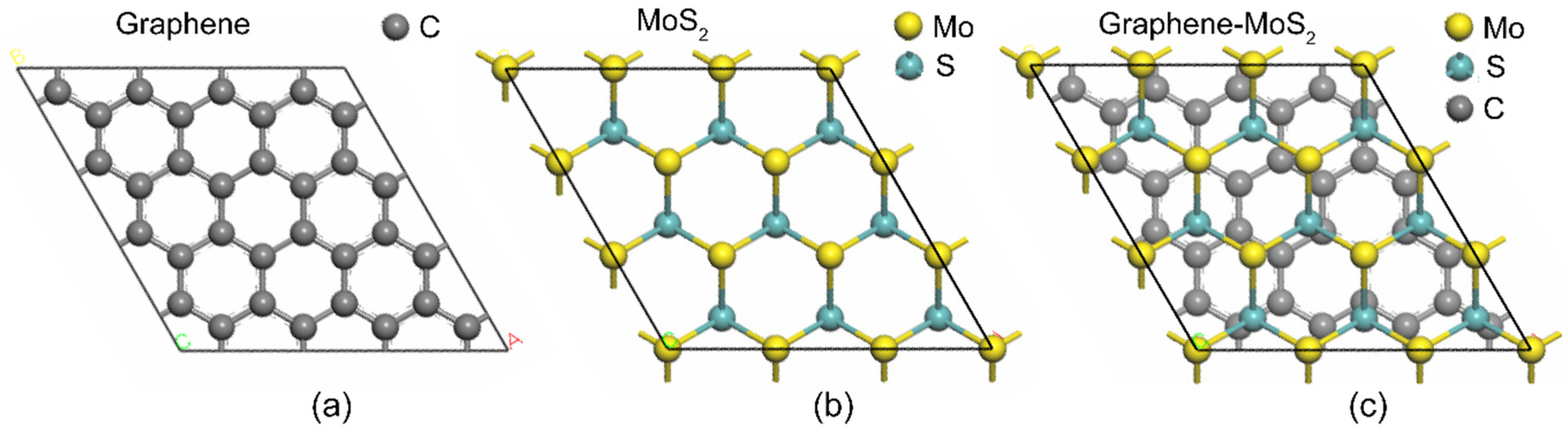
First principles calculation was performed in the framework of DFT as implemented in the Cambridge Serial Total Energy Package (CASTEP) simulation software. Suitable choice of functional parameters is important for geometrical optimization and properties calculations. From the convergence test results, the Perdew-Burke Ernzerhof (PBE) exchange-correlation functional with general gradient approximation (GGA) functional was taken for electron exchange and correlation. Ultra-soft pseudopotential was employed for the calculations of electronic interaction with 12 valence electrons of Mo (4
p6, 5
s1, 4
d5), six valence electrons of S (3
s2, 3
p4), and four valence electrons of C (2
s2, 2
p2). The plane-wave functions basis set with cut-off energy limited at 380 eV as increasing the value to 400 eV did not give any significant change in the total energy of the system. All atomic positions in the supercell have been relaxed according to the cell optimization criterion, such as displacement of 5.0 × 10
−4 Å, force of 0.01 eV/Å, and self-consistency field (SCF) tolerance of 5.0 × 10
−6 eV/atom. The plane-wave Monkhorst-Pack k-point was sampled by 4 × 4 × 1 for the relaxation and total energy calculations. The optimized model structure of graphene-MoS
2 was constructed using a 4 × 4 graphene and 3 × 3 MoS
2 supercell with a vacuum slab of 15 Å to have a smaller lattice mismatch and prevent periodic interaction. Some selected criteria and values were adopted from available literature [
7,
21,
22] as guided references. A small supercell with adequate atomic number was employed as larger supercell consumes more time and computational cost for DFT calculation to be done. The simple model of atomic structure for graphene, MoS
2, and graphene-MoS
2 are shown in
Figure 1a, 1b, and 1c, respectively. Graphene consists of hexagonal bonded carbon atoms, while MoS
2 consists of S-Mo-S layer with Molybdenum (Mo) atoms arranged in trigonal prismatic coordination between the two Sulphur (S) layers. Meanwhile, the optimized atomic configuration of graphene-MoS
2 was confirmed with previous study by [
21,
22]. The adjacent layers of the heterostructure are held together by vdW force at the selected active site.
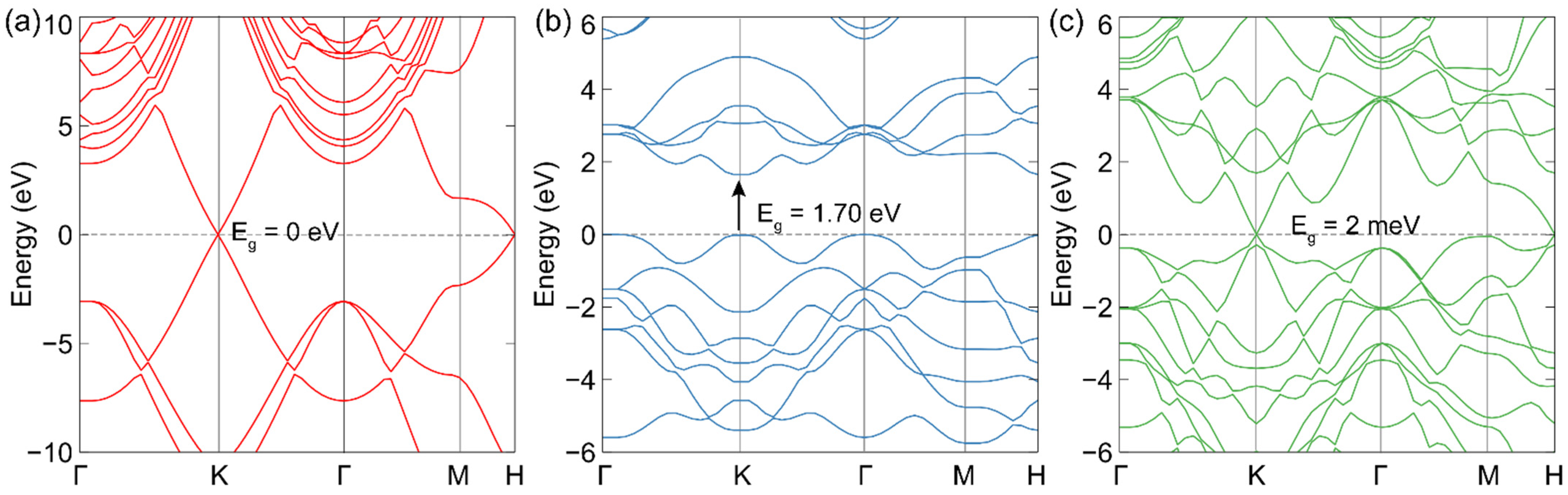
In order to explore the electronic structure properties of graphene-MoS
2, DFT calculations on typical electronic band structures have been performed and illustrated in
Figure 2. The band structures were plotted along the high symmetry point in Brillouin zone (BZ) to observe the energy band gap (E
g). The E
g can be determined by the opening gap between valence band maximum (VBM) and conduction band minimum (CBM) of occupied state presented in band structure with Fermi level equal to zero. As shown in
Figure 2a, graphene exhibits a gapless nature with formation of Dirac cone at the Fermi level. The zero-energy band gap of graphene was in excellent agreement with other reported work in literature [
7,
21,
22]. Theoretically, due to zero gap, electrons and holes inside atomic structure can freely move, thus resulting in fast carrier dynamics and broad wavelength coverage as it possesses wavelength-independent absorption [
7].
Meanwhile pure monolayer MoS
2 shows a direct band gap with value of 1.70 eV which is consistent with other theoretical report ~1.8 eV [
23], ~1.73 eV [
24] and ~1.7 eV [
25]. Upon hybridization of graphene and MoS
2, the VBM and CBM are situated along the high symmetry K point of BZ, confirming the direct type of band gap with a small magnitude equal to 2 meV. The calculated band gap value has been validated with previous theoretical study, which is 8.3 meV [
21], 3.6 meV [
22], 0.4–1.1 meV [
23], 3.49 [
24] and 27 meV [
8]. In principle, a direct band gap materials are optically active semiconductor, thus making them preferable in most photonic devices, while the indirect gap compounds show relatively less optical excitation and emission as the transition is associated with phonon energy [
25]. The Dirac properties of graphene is also preserved near the Fermi level even with the modulation in band gap energy, as shown in
Figure 2c. From the result, the band gap tuning can be attributed to the increase in crystallinity due to the variation of the interlayer coupling strength, resulting in higher atoms mobility with MoS
2 acting as the transition metal material donating the holes to the graphene [
23,
26]. The existence of energy gap in band structure can entail optical absorption edge which corresponds to the intra- and inter-band electron transitions from occupied to unoccupied states. The charge transfer and quantum confinement between two hybrid materials thereby making them optically active.
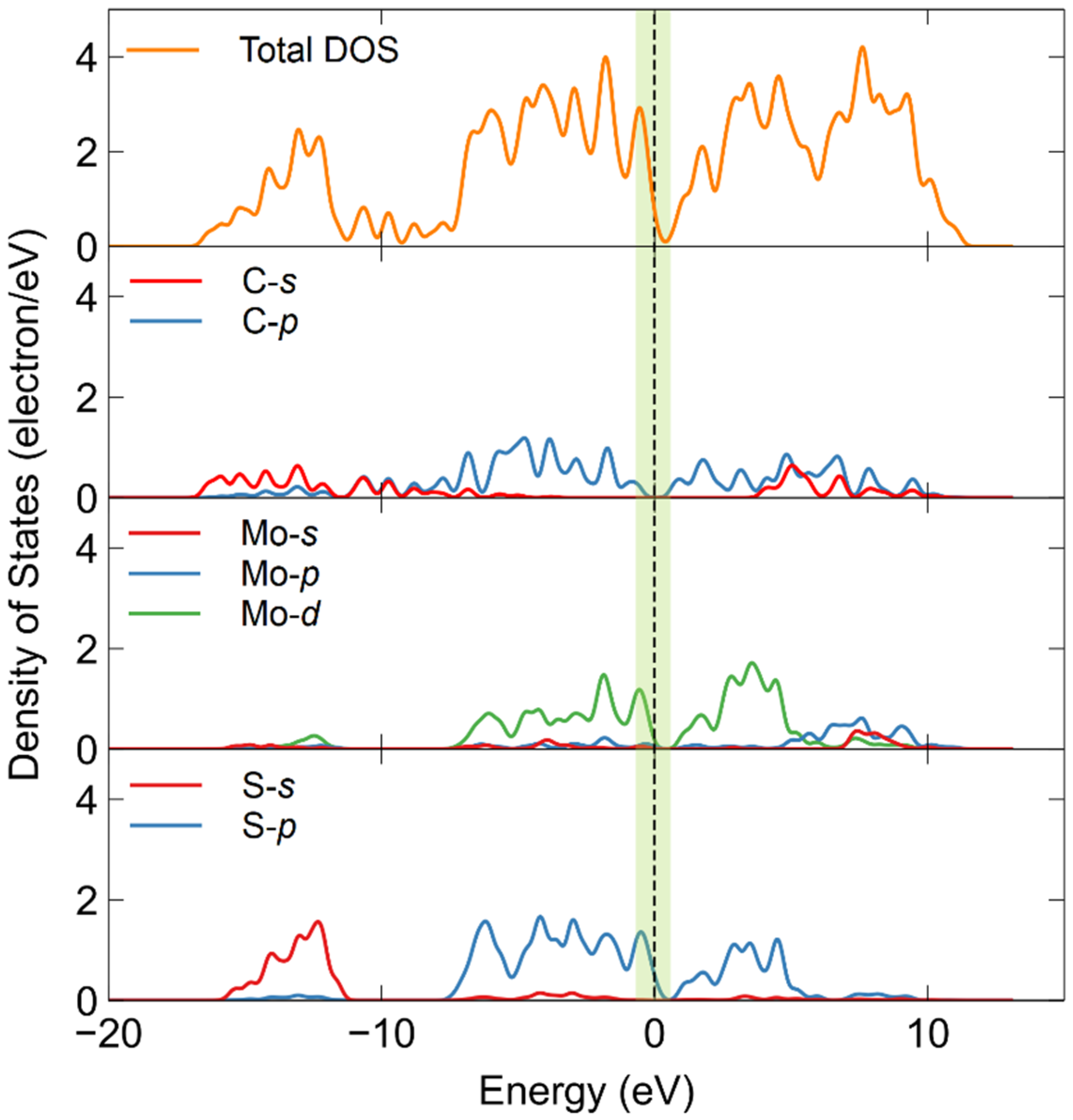
In addition, the investigation on the origin of band structure for graphene-MoS
2 is required to identify the contribution of electronic states from different orbital of the constituent atoms. Therefore, the total and partial density of states (DOS) of graphene-MoS
2 is computed and illustrated in
Figure 3. The green box highlighted in the
Figure 3 is where Fermi level and band gap is located inside atomic structure. It is demonstrated that the prevailing contribution to the total DOS at the VBM is primarily from the upshifted of Mo-
d and S-
p orbital of MoS
2. The
d and
p orbital are the lowest electronic state in the atomic arrangement of MoS
2, which signifies the active optical elements and is mainly responsible for the electronic transition inside the band gap [
22]. Meanwhile, the DOS for graphene preserved its Dirac property near the Fermi level. Therefore, the band gap of graphene hybrid can be tuned through the variation in MoS
2 concentration to determine an optimized ratio in hybridization materials [
17,
22].
Optical characterization can be modelled by the complex dielectric function of the material system derived from the Kramers-Kronig relation, ε(ω) = ε
real + ε
imaginary with function of photon energy (ω) [
25]. The real part of dielectric constant is complex permittivity associated with polarization of light caused by the applied electric field, while the imaginary part is related to the optical absorption of photon (loss or gain) of the material [
13,
14]. The equation can be expanded to other optical constants such as refractive index, absorption coefficient, reflectivity, and energy loss spectrum. The simulated real and imaginary parts of dielectric function of graphene, MoS
2, and graphene-MoS
2 are shown in
Figure 4a,b. The dielectric functions of graphene and MoS
2 material have highly anisotropic properties at low energy regions and become isotropic towards high energy region, which is similar to other studies [
24,
27]. Since optical constant is wavelength dependent, low energy zone ranging from infrared, visible to ultraviolet region is more preferable to be explored, particularly at telecommunication region of 1550 nm or 0.8 eV for photonics application.
The value of static dielectric constant of pure graphene at 0.8 eV was 4.2, with prominent peak at 2.0 eV. The simulated result showed an agreement with previous study by Qiu et al. [
24] that obtained the same trend with value of dielectric constant about 4.5 at low energy region and significant peak at 2.5 eV. For imaginary part, a significant peak at 3 eV was observed, which originates from the inter-band transitions according to the interpretation by previous reported work [
27]. The same trend can be seen for dielectric function of MoS
2 structure, except it has a high dielectric constant value at 0.8 eV, which is about 12.4 with prominent peak at 4.0 eV. The value is consistent with previous reported work by Hieu et al. [
25], which records dielectric value of 15.01 and significant peak at 3.5 eV. Meanwhile, as graphene and MoS
2 were stacked together, the dielectric constant was modulated to a value of 14.4 and significant peak at 1.6 eV. The transition of real part from positive to negative intersect at 3.1 eV indicate that graphene-MoS
2 should resonate at energy higher than that 3.1 eV [
26]. The imaginary part shows an increase of spectrum compare to the individual graphene plots, which is reflected to the rise of electronic interaction inside the material [
24]. This imaginary part is directly providing the absorption spectra analysis, which has been further illustrated in
Figure 5.
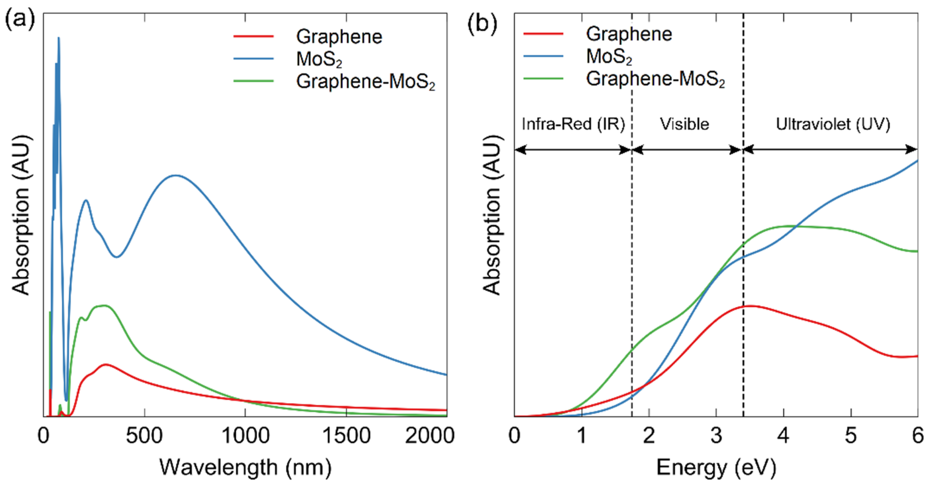
Figure 5a shows the simulated absorption spectrum with respect to wavelength and photon energy in the inset. The absorption peak at 225 nm from graphene corresponds to the typical π-π* transition of aromatic C–C bonds in the graphene network [
28]. Similar trend can be observed when MoS
2 is incorporated into graphene network with larger absorption peak. The increase in absorption peak indicates the absorption properties of graphene was preserved but exhibit a greater conjugated π bonds at the increased material concentration as described by Beer-Lambert law relation [
29]. For MoS
2, the absorption spectrum consists of characteristic peaks at around 400–450 nm ascribed from the excitonic transitions within high-density of states in Brillouin zone [
30].
In parallel, absorption spectrum with respect to energy was shown in
Figure 5b to confirm the accessible wavelength region for the three models’ structures. The absorption intensity of graphene was recorded as the lowest with broadest spectrum covering from infrared to ultraviolet region. This is in agreement with the well-known broadband wavelength range from the optical characteristic of graphene [
1,
2,
3]. The results also agree with the absorption spectrum at low energy region below 2 eV as reported by Qiu et al. [
22]. Meanwhile, optical absorption coefficient can be obtained from the absorption edge at the intersection of reverse tangent and
x-axis of lower energy region. It corresponds to the electronic transition inside the materials with binding energy and describes optical gap of material. The simulated optical gap of graphene, MoS
2, and graphene-MoS
2 is 0.45 eV, 1.62 eV, and 0.69 eV, respectively. The values were comparable with the data from previous work [
24], which recorded optical gap of 0.75 eV for graphene, 1.63 eV for MoS
2, and around 0.41 eV to 1.40 eV for graphene-MoS
2. The optical gap of graphene-MoS
2 was averagely low, allowing the photoelectron to be excited with less energy [
24,
28]. Besides that, the calculated absorption spectrum proved that hybrid of graphene-MoS
2 possesses a broadband wavelength range from infrared, visible to ultraviolet regions with significant increase in absorption intensity compare to individual graphene, leading to a widespread application.
3. Material Fabrication and Characterization
Three samples were fabricated, which are graphene-MoS
2, graphene, and MoS
2 with chitin as a host polymer to form SA film and the process is as follows. Graphene filament was employed as the starting material for the preparation of graphene suspension. Initially, graphene-polylactic acid (PLA) filament (Conductive Graphene Composites, Black Magic 3D) with a diameter of 0.4 mm was extruded through a 3D printer nozzle to reduce its diameter to a desired 400 µm for easier processing. The composition of the filament consists of graphene platelets (30–40%), polylactic acid (25–35%), Tris(nonyl phenyl)phosphite (5–10%), and carbon fibers (5–10%) which can be retrieved from
blackmagic3D.com [
31] website. The extruded filament was weighed at approximately 25 mg and added into 10 mL of tetrahydrofuran (THF), producing graphene slurry in THF solution. The graphene-PLA-THF suspension then underwent ultrasonication in ultrasonic bath for 10 min. For MoS
2 suspension, 5 mg of MoS
2 powder (Sigma Aldrich, St. Louis, MO, USA, particles diameter of ~100 nm, purity 99%) was dissolved homogeneously in 5 mL of THF solution under magnetic stirring at ambient temperature and 1000 rpm for about two hours.
Extraction process of chitin biopolymer used in this research was based on Wan Nawawi et al. [
32]. Chitin nanofiber was extracted from frozen oyster mushrooms (
Pleurotus ostreatus) using mild alkaline treatment to preserve the amorphous glucans within the matrix. The frozen mushrooms were thawed and blended for 5 min with a high-speed mixer (Vita Mixer Innofood, SX766) to break the cell wall. After that, water-soluble components were removed by hot water treatment under stirring conditions (85 °C, one hour). The suspension was filtered with a cotton filter cloth before the wet cake was being left to soak in 1 M sodium hydroxide for 3 h at 65 °C. The suspension was then neutralized using the filtration process and the neutralized wet cake was diluted with distilled water (0.4%
w/
v). For homogenous dispersion, the chitin dilution was post-blended for 5 min and kept stable at 4 °C until further use.
Solution-process of graphene-MoS
2 hybrid was done by mixing an equal amount of 1.25 mL graphene and MoS
2 solution into 2.5 mL of chitin biopolymer. Altogether, the ratio of graphene-MoS
2 to chitin is 1:1 ratio summing up to 5 mL in volume. The 5 mL value was chosen to ensure the solution could be filled into the circular petri dish with 3.5 cm diameter and 1.0 cm height producing film with thickness of around 30 µm to 50 µm. Then, the mixed solution was placed in ultrasonic bath for about three hours to ensure a well-homogenized dispersion. Ample time of sonication process allowed exfoliation of bulk crystals into nanosheets as the van der Waals interaction weakened due to production of microjets and shockwaves from collapsing cavitation bubble [
33]. The obtained dispersion mixture was then poured into a petri dish and let dry at ambient temperature for about 48 h before they were ready to be peeled off as a free-standing film SA. Meanwhile, individual graphene-chitin SA was fabricated by mixing homogeneous graphene-PLA-THF with chitin in 1:1 ratio, sonicated in ultrasonic bath for two hours and poured into petri dish before letting dry for two days. At the same time, by using the same process, the homogeneous MoS
2-THF suspension was mixed with chitin in 1:1 ratio to produce MoS
2-chitin based SA.
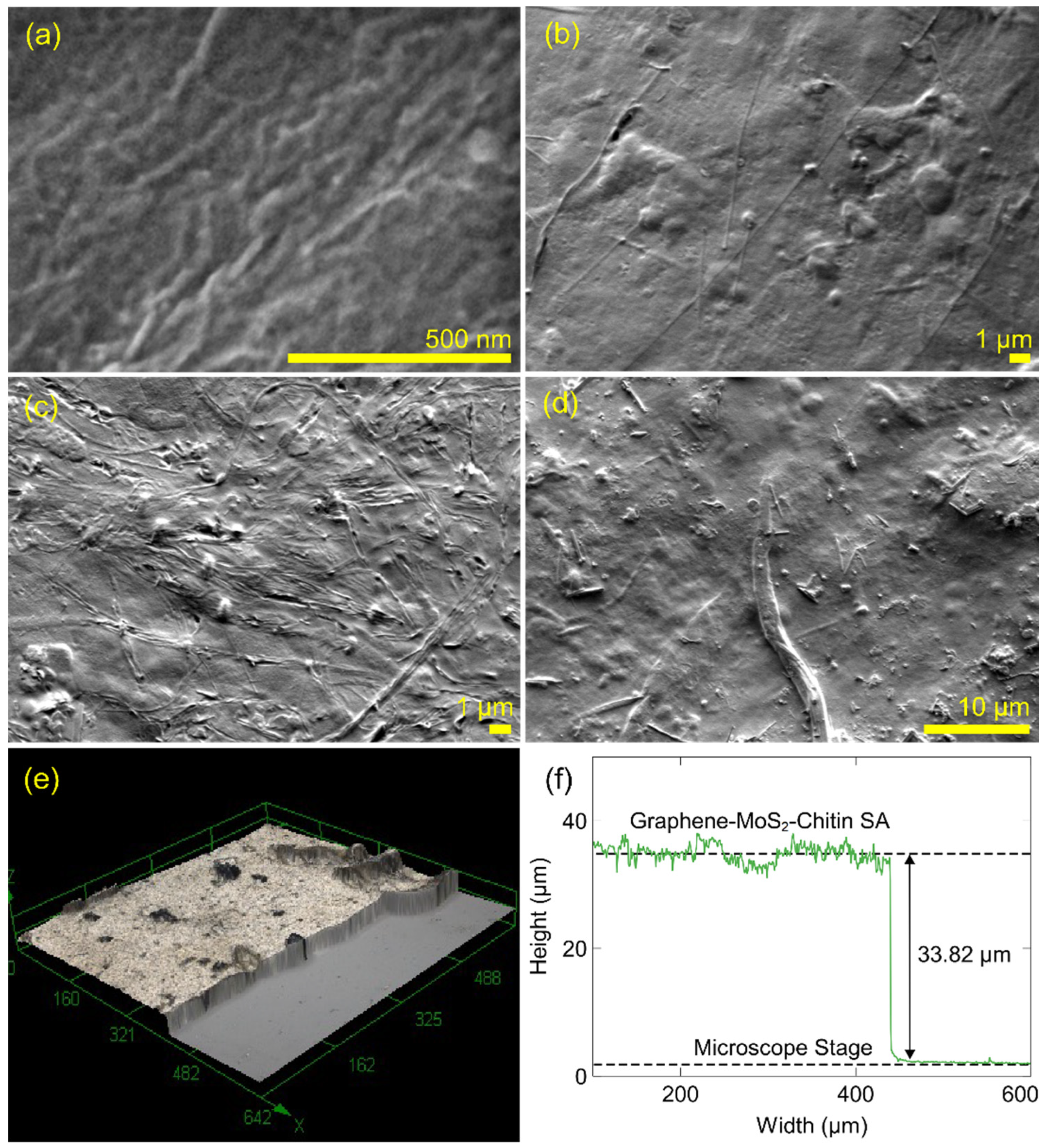
The SA films undergo structural characteristic evaluation before further demonstration of their effectiveness in pulsed fiber laser operation. The morphology of extracted fungal chitin was observed using field emission electron microscope (FESEM) (Hitachi, Tokyo, Japan, SU 8030) at 1 kV accelerating voltage, while graphene-chitin, MoS
2-chitin, and graphene-MoS
2-chitin were observed from model JSM-7800F (JEOL, Tokyo, Japan).
Figure 6a highlighted the fibrous structure of chitin with blurry image contributed by the amorphous structure of glucans that bind a dense network of fibers. As chitin becomes polymer for all developed samples, the fibrous network with tube or string-like formation and large surface area of flaky image dominates the whole composition surface as can be observed in
Figure 6b–d. This is denoted to the material embedded uniformly into the chitin bio-host polymer. In addition, all obtained FESEM image denotes a uniform distribution with no bubbles, hole, or crack which is vital for material’s performance in terms of ensuring lower amplitude fluctuations during pulse laser generation [
1].
Figure 6e,f shows the thickness profile of graphene-MoS
2-chitin which was measured using 3D laser scanning microscope (Olympus, Tokyo, Japan, OLS 4100). The thickness was measured by the difference in height of the graphene-MoS
2-chitin and microscope stage. The measured thickness is around 33.82 µm which is consistent with other reported film thickness of around 30–50 µm [
34]. In addition, the thickness of the graphene-chitin and MoS
2-chitin should be similar with the graphene-MoS
2-chitin due to the thickness of the SA is determine by the amount of sample solution before dry casting process.
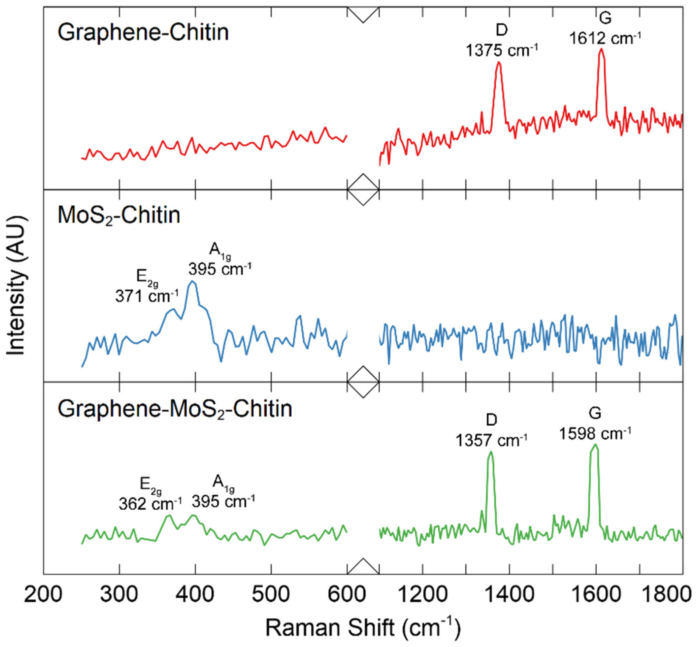
Figure 7 reveals the Raman spectrum of the fabricated film which will confirm the materials’ existence through key spectrum peaks identifiers resulted from the vibrational modes of material. In pure graphene Raman spectrum, due to the vibration of sp
2-bonded carbon atoms, the two prominent characteristic peaks of D-band and G-band of graphene layer at 1390 cm
−1 and 1584 cm
−1 are clearly displayed in the figure. The single layer graphene can be analysed from the peak intensity ratio of the 2D and G is equal to 2 or expressed by I
2D/I
G = 2 [
35]. This expression is true if the graphene has sharp symmetric peak, which confirms the high quality and defect-free graphene sample. Since the obtained peak from the Raman spectrum is not sharp and symmetric, this indicates that the developed graphene is not defect-free and has relatively high number of layers produced. The fact that LPE method is employed, it is worth mentioning that structural defect cannot be avoided. Nevertheless, we had successfully confirmed the graphene existence in the sample through the Raman spectrum. Meanwhile, Raman peaks at E
2g and A
1g which are the characteristic peaks of the 2H-phase MoS
2 are confirmed at 376.59 cm
−1 and 395.71 cm
−1 respectively. For graphene-MoS
2 nanocomposite, the corresponding two significant peaks at 1357.03 cm
−1 and 1574.58 cm
−1 are in agreement with previous reported study [
36]. As MoS
2 is introduced in graphene matrices, the G-band of graphene is down-shifted to 1574.58 cm
−1 as a result of the softening of the atomic bond with addition of doping which also reveals the evidence of interlayer coupling inside the nanocomposite [
36].
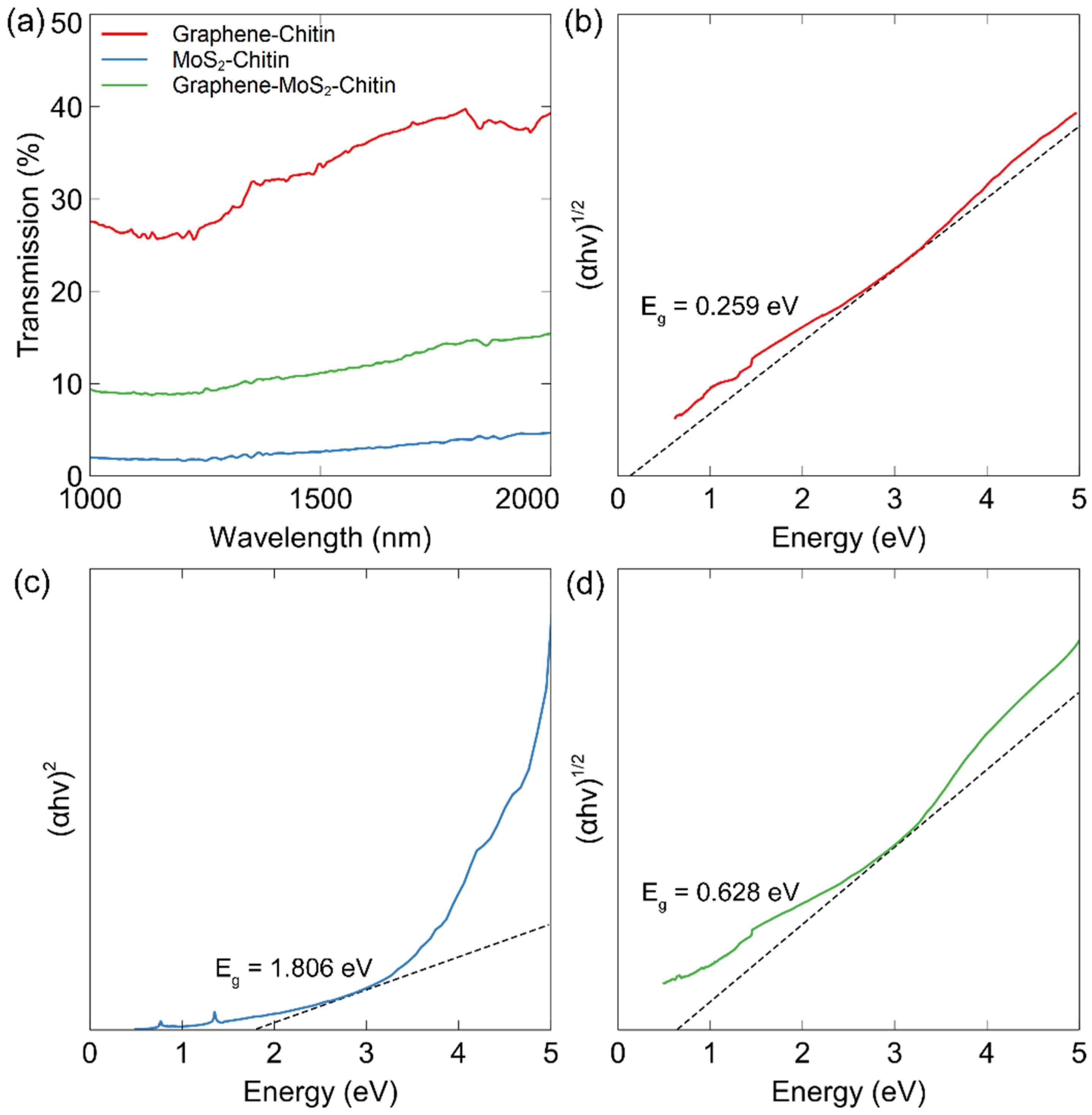
Figure 8a shows the ultraviolet-visible-near infrared (UV-Vis-NIR) (Perkin-Elmer, Waltham, MA, USA, Lambda 750) transmission spectrum of graphene-MoS
2, graphene and MoS
2 film to investigate the optical absorption and transmission response of the prepared materials. The transmission of 11.54% was recorded at a wavelength of 1550 nm for graphene-MoS
2 film which is lower than that of graphene (~33%) but higher than MoS
2 (~3%). The obtained value depicts that the incident light passing through the graphene-MoS
2-chitin SA was reduced due to heightened absorption ability has been achieved. From the UV-Vis-NIR spectrum, the optical bandgap can be obtained by using Tauc plot method in which (
αhv)
n was plotted as a function of photon energy (
hv) where
α is the linear absorption coefficient,
hv is the incident photon energy and
n can be ½ or 2 for a direct and indirect allowed transition, respectively [
37]. As shown in the
Figure 8b–d, the linear fitting interception at
x-axis and by fitting the suitable values of
n in the Tauc relation gives the bandgap value. Based on the linear intercept, the value of band gap is comparable with those theoretical value obtained from the band structure in
Figure 2. From the
n value, both Graphene-MoS
2 and graphene has direct bandgap of 0.628 eV and 0.259 eV respectively. Meanwhile, MoS
2 exhibit indirect band gap of 1.806 eV. It is expected that experimental value for graphene, MoS
2 and graphene-MoS
2 are slightly different from theoretical simulation mainly arises from the additional composition of the host polymer material such as chitin and the inevitably impurities throughout the fabrication process. Nevertheless, the result of Tauc relation is in agreement with the theoretical band structure in determining direct and indirect energy gap.
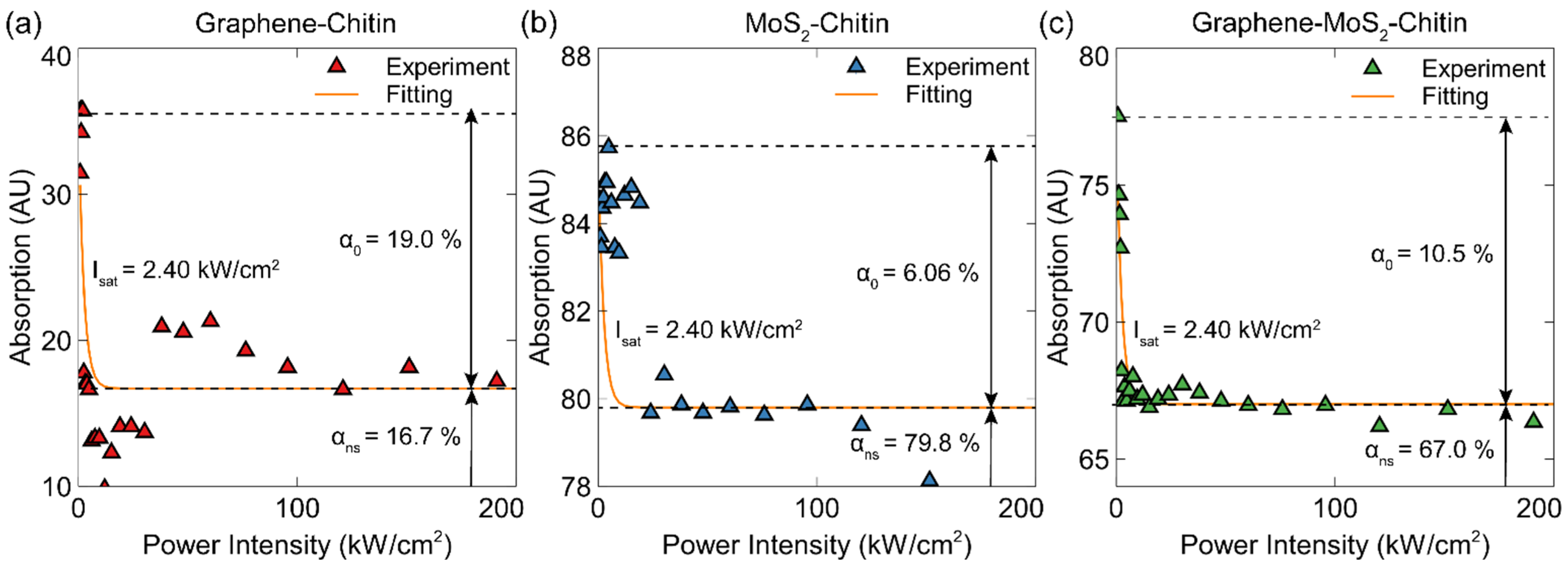
The nonlinear absorption properties of the graphene-MoS
2 nanocomposite SA were investigated by a balanced twin detector method. In the measurement, the nanosecond pulse fiber laser with repetition rate of 1.89 MHz and pulse width of 191.6 ns was used as a light source.
Figure 9 shows the experimental data and curves fitted by the following equation;
where
A,
I,
α0, Isat, and
αns is absorption, input intensity, saturable absorption (modulation depth), saturation intensity, and non-saturable absorbance coefficient respectively [
38]. As shown in
Figure 9, the highest modulation depth is shown by individual graphene at 19.0%, higher compared to previous graphene-based SA [
39]. Meanwhile, graphene-MoS
2 SA has modulation depth of 10.5% with saturation absorption intensity of 2.40 kW/cm
2. The lowest modulation depth at around 6.06% is achieved by individual MoS
2 with saturation intensity of 2.40 kW/cm
2.
4. Fiber Laser Setup and Nanosecond Pulse Performance
The fabricated SA film was integrated into an EDFL ring cavity by sandwiching it between two ferrules, as shown in
Figure 10. The ring cavity consists of additional 100 m long standard single mode fiber (SMF) to tailor the dispersion characteristic and nonlinearity of the cavity, thus allowing a nanosecond pulse generation with the extension of the cavity length. The EDFL cavity works in anomalous dispersion with net total dispersion at around ~2.25 ps
2/km. The output was tapped out by a 90/10 optical coupler, where 90% of the light is kept oscillating in the cavity, and the remaining 10% is used for output measurement to simultaneously observe the pulse train, signal-to-noise ratio, and optical spectrum through a 10 dB coupler. The laser outputs were obtained through an optical spectrum analyzer (Ando, Kanagawa, Japan, AQ-6370C) for optical spectrum trace and optical power meter (OPM, Thorlab, Newton, NJ, USA, PM100D) for output power measurement. A 5 GHz photodetector (Thorlab, DET08C) was connected to 500-MHz digital oscilloscope (GW Instek, New Taipei City, Taiwan, GDS3352) for pulse train and a 7.8 GHz Radio Frequency (RF) spectrum analyzer (Anritsu, Kanagawa, Japan, MS2683A) for signal-to-noise ratio (SNR) measurement. The overall length of this laser cavity was approximately 110 m.
The performance of the pulsed laser generation was investigated by varying the 980 nm input pump power. Except for MoS
2-chitin, the developed SAs are able to realize nanosecond pulsed laser. Therefore, presented here are the nanosecond pulsed laser performance for graphene-chitin and graphene-MoS
2-chitin and Q-switched pulsed laser for MoS
2-chitin.
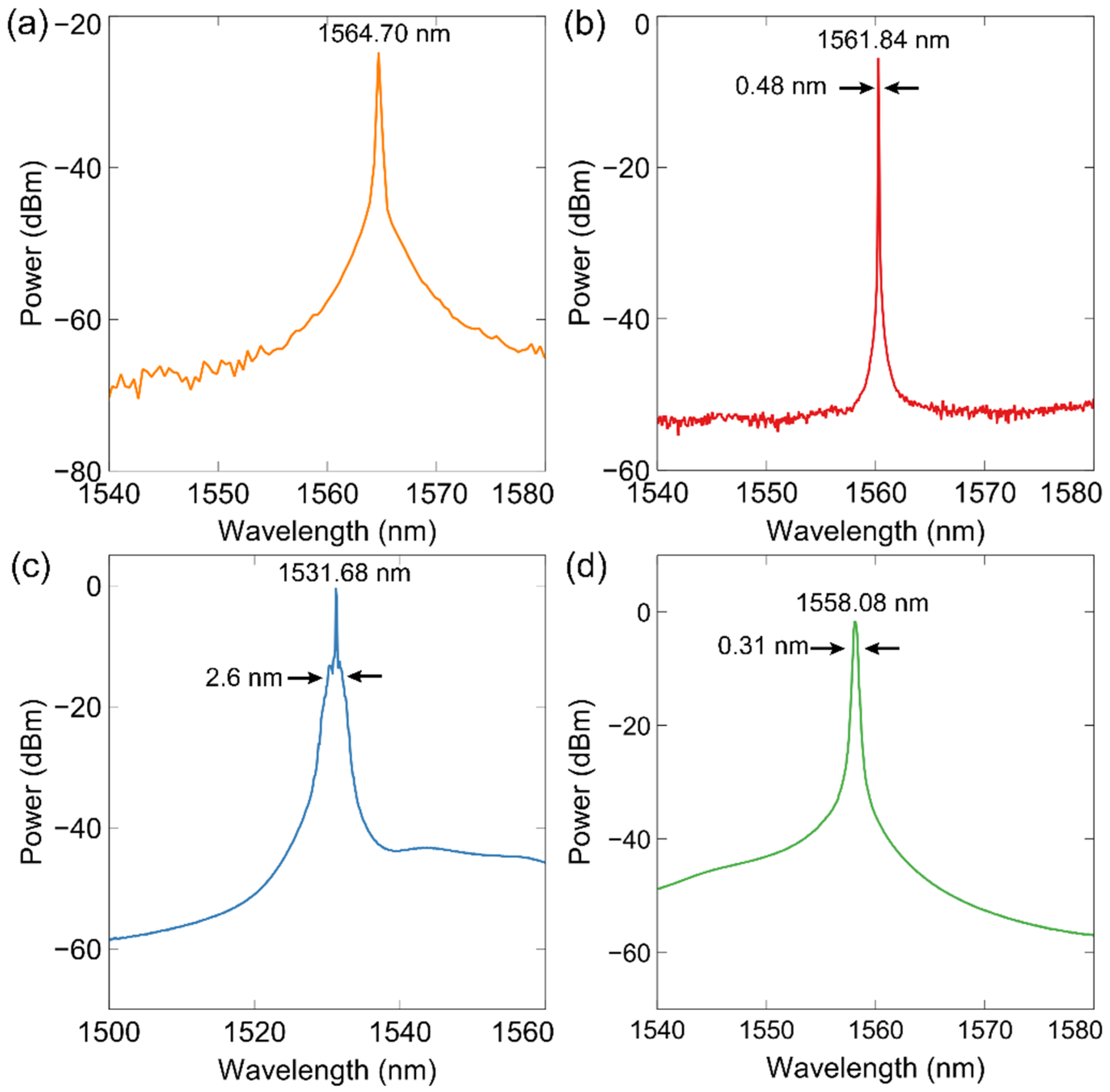
Figure 11 shows the OSA trace for the developed SAs compared to the continuous wave (CW) spectrum. The CW wavelength was recorded at 1564.70 nm as depicted in
Figure 11a. When the SAs were inserted in the cavity, the wavelength showed some shift as can be seen in
Figure 11b–d for graphene-chitin, MoS
2-chitin, and graphene-MoS
2-chitin, respectively. At maximum pump power of 75.91 mW, the graphene-chitin SA exhibited an almost similar wavelength (~1564 nm) with graphene composite fabricated via electrochemical exfoliation proposed by Ismail et al. [
39]. The operating wavelength of 1561.84 nm for graphene-chitin SA showed a slight shift from the CW with spectrum broadening of 0.48 nm as shown in
Figure 11b.
A broad wavelength spectrum can also be observed when using graphene-MoS
2-chitin based SA with spectral bandwidth of 0.31 nm at 1558.08 nm central wavelength. The observed optical spectrum broadening can be inferred to the self-phase modulation effect in the laser cavity and the nanosecond operation of the EDFL. Meanwhile, MoS
2-chitin based SA produced a broad wavelength of 1531.68 nm with a sharp peak due to parasitic lasing as shown in
Figure 11c. Parasitic lasing is an uncontrolled lasing resulting from the internal reflection of light inside laser system, thereby making a highly unsaturated laser gain during pumping period [
40]. It can also relate to the uneven dispersion and surface condition of the material [
41]. The optical spectrum that exhibits parasitic lasing can reduce the reliability of a high-gain laser [
40]. This could probably be one of the hindering factors in generating nanosecond pulsed laser using this specific SA. The low saturable absorption of MoS
2-chitin SA (as observed in
Figure 9b) cannot provide enough gain to produce sufficient optical power and overcome the parasitic lasing [
41].
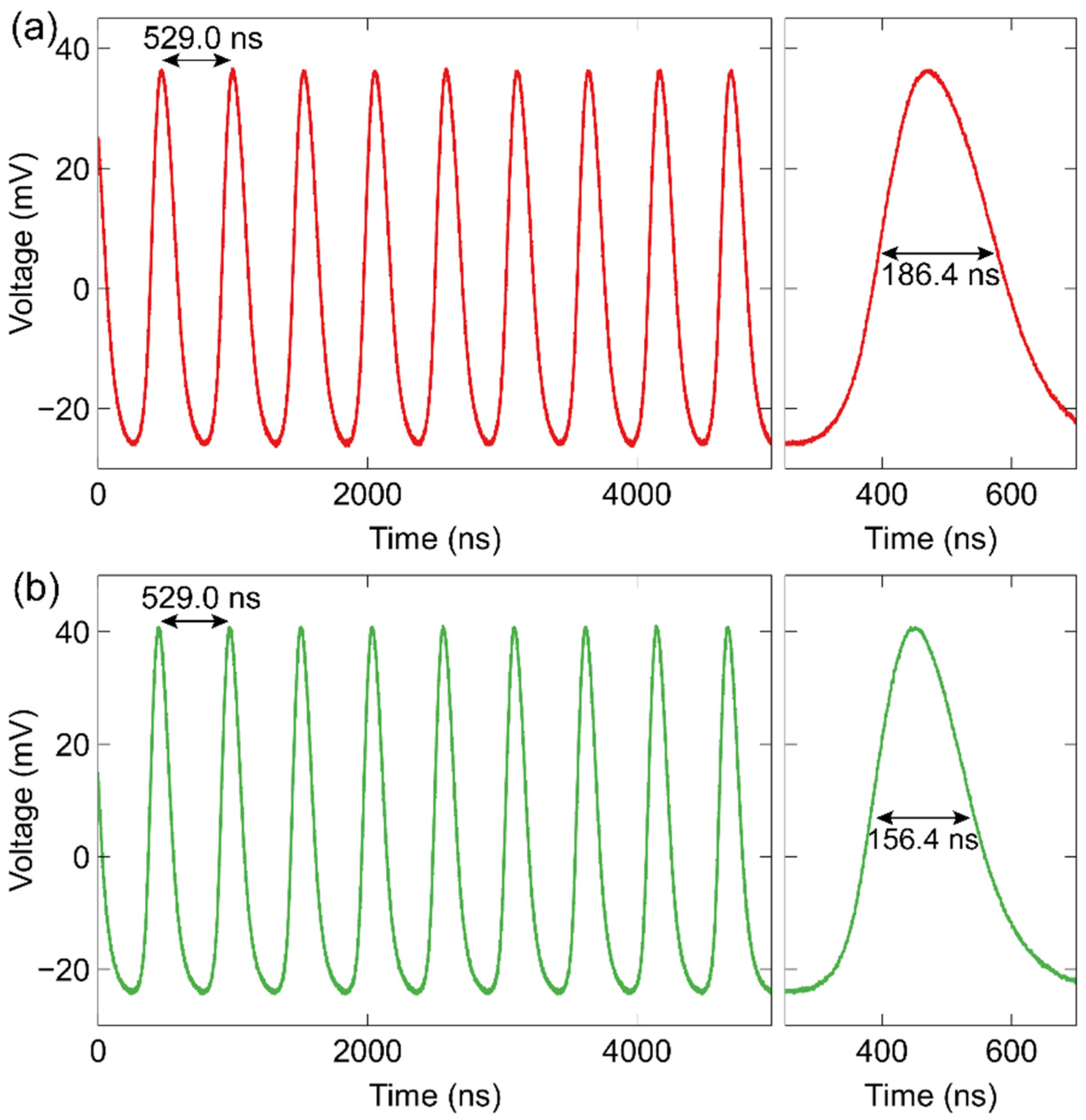
A stable self-started nanosecond pulse was obtained as the input pump power was increased gradually above the threshold of 40.29 mW until 111.52 mW for graphene-MoS
2-chitin and 35.20 mW until 75.91 mW for graphene-chitin. The threshold pump power is relatively high due to the insertion loss of the SA film and the long cavity. As the pump power was further increased, both SA films were observed to maintain their stability without any thermal damage. The stable repetition rate and pulse width were achieved, which denotes that the nanosecond pulse laser operation was able to be maintained until the maximum pump power. Repetition rate of graphene-chitin and graphene-MoS
2-chitin SA was recorded at a similar frequency of 1.89 MHz. This is because the repetition rate is dependent to the length of laser cavity. The oscilloscope trace of the pulse train as illustrated in
Figure 12a,b, demonstrated that the time interval between the pulses is about 529 ns, equal to 1.89 MHz which corresponds to the cavity length of 110 m. The shortest pulse width was achieved by graphene-MoS
2-chitin at 156.4 ns and was maintained when adjusting the input pump power from 40.29 mW to 111.52 mW. The recorded nanosecond pulse width is also lower than previous reported SA based on single-walled carbon nanotube (SWCNT) by drop-cast technique at 332 ns [
42], zinc oxide-polyvinyl alcohol (PVA) at 400 ns [
43], silver nanoparticle-polyvinyl alcohol (AgNP-PVA) at 202 ns [
44] and copper nanowires-polydimethylsiloxane (CuNWs-PDMS) film at 173 ns [
45] indicating that the developed hybrid graphene SA yielded better performance for nanosecond pulsed laser in EDFL. In comparison with its single component, graphene-chitin has slightly longer pulse width of 186.4 ns, but still shorter than graphene-polyethylene oxide (graphene-PEO) developed by another work [
39] that records 400 ns pulse width.
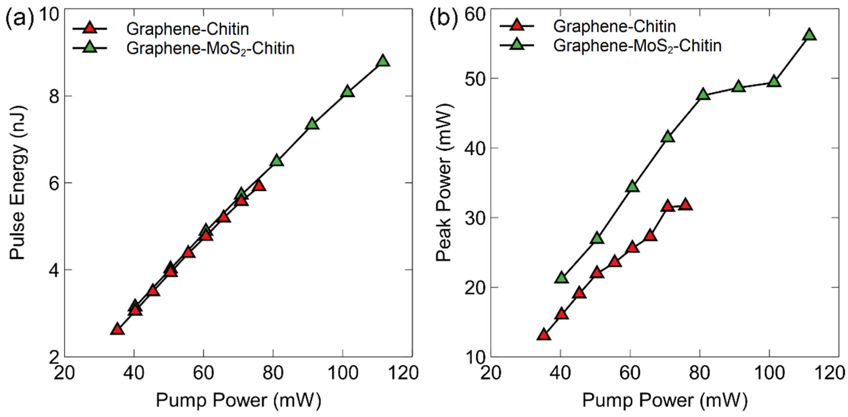
Figure 13a,b show the average output power and pulse energy of the generated laser pulses against pump power. The output power was observed to have a typical increasing trend with the corresponding pump power. At maximum pump power, peak power and pulse energy recorded by graphene-chitin are 31.71 mW and 5.91 nJ respectively, five times higher than graphene-PEO based SA proposed by Ismail et al., [
39] that recorded at about 1.739 mW and 1.79 nJ. Meanwhile, a higher value of peak power and pulse energy was achieved by graphene-MoS
2 than individual graphene-based SA at maximum pump power which was recorded at 56.13 mW and 8.78 nJ respectively. The results demonstrated that the hybrid graphene could generate high-energy pulsed lasers at a high incident laser pump.
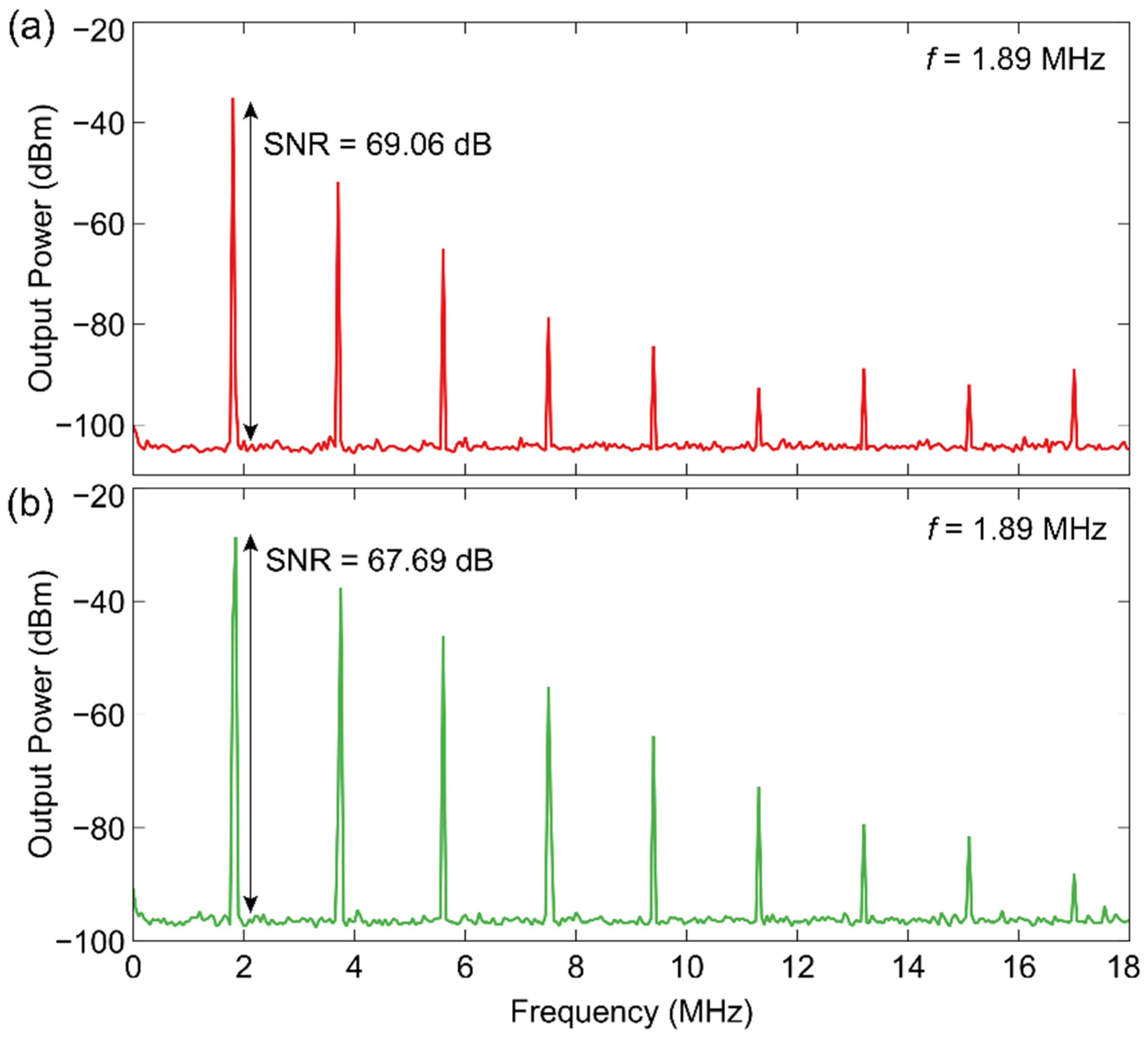
Besides, the stability of the pulsed laser was analysed based on the RF spectrum obtained from the RF spectrum analyser as shown in
Figure 14a,b. The RF spectrum for both developed SAs show high signal-to-noise ratio (SNR) above ~60 dB which indicate the stability of the pulses with no signal inconsistency. The plotted result also demonstrated the fundamental frequency of 1.89 MHz that matches with the peak-to-peak duration of the oscilloscope pulse period. The SNR value recorded by graphene-chitin and graphene-MoS
2-chitin were 69.06 dB and 67.69 dB respectively, higher than graphene-PEO (57.3 dB) [
39], SWCNT (36 dB) [
42], ZnO-PVA (64 dB) [
43], and CuNWs-PDMS (61 dB) [
45]. These results suggest that graphene-MoS
2-chitin hybrid developed through LPE method could be as an effective SA for nanosecond pulse generation and exhibit better SA performance compared to previous reported works [
39,
42,
43,
44,
45]. Finally, the performance of the proposed SA is compared with recent publication of nanosecond EDFL as summarized in
Table 1. These results verified the ability of graphene-MoS
2-chitin SA film to generate nanosecond pulsed lasers and their potential applications in optoelectronic devices.
The developed MoS
2-chitin SA yielded a stable Q-switched pulsed laser in the same laser cavity.
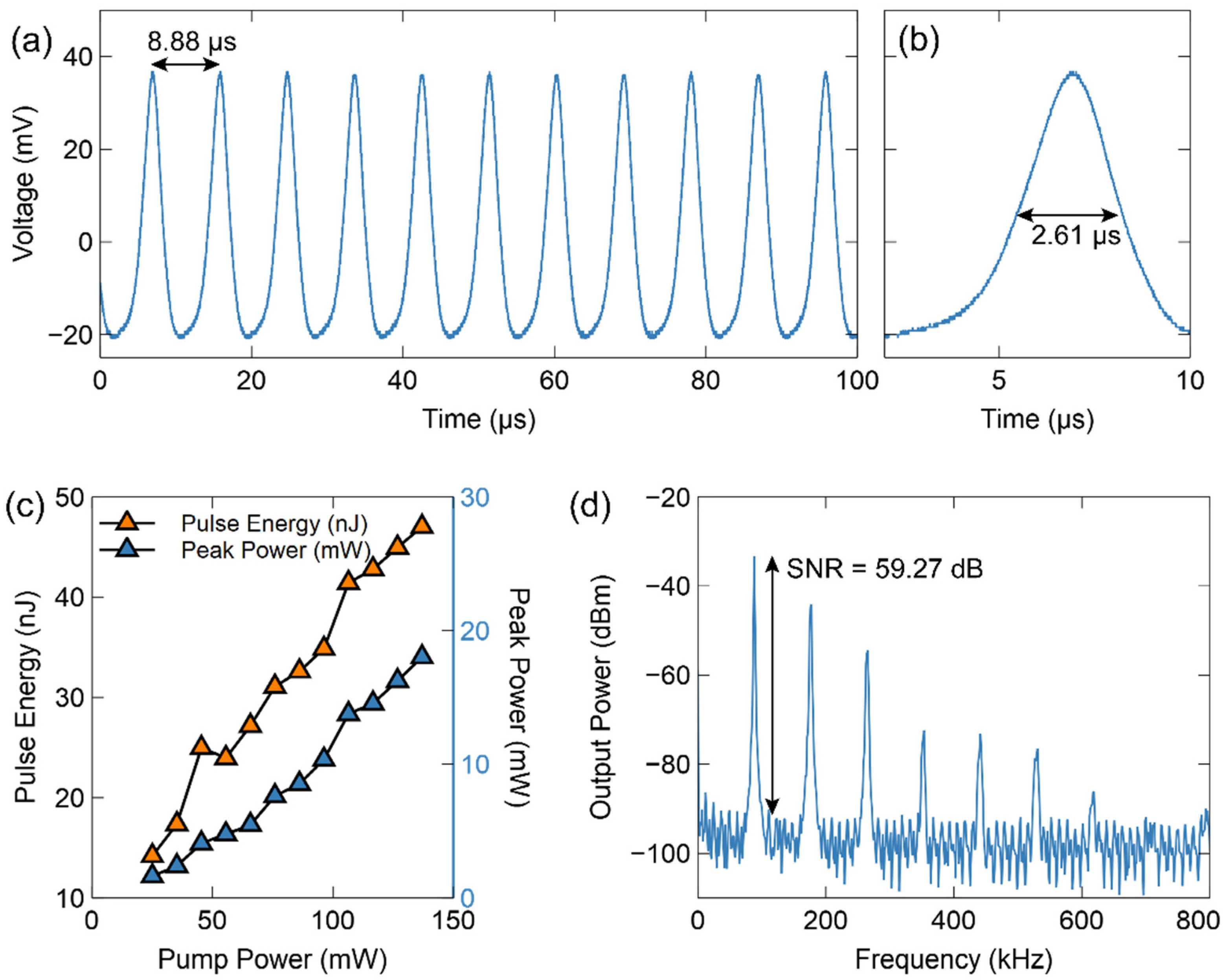
Figure 15 shows the laser characterisation of MoS
2-chitin SA. At maximum pump power of 136.96 mW, a high repetition rate of 112.3 kHz with very small amplitude jitters and pulse width of 2.61 μs were recorded. The repetition rate was by far the highest recorded value compared to other reported works developed by liquid-phase exfoliation and mechanical exfoliation approach, which is 27.0 kHz [
46], 38.43 kHz [
47], and 43.47 kHz [
48]. A typical Q-switched operation can be observed from the ascending trend of pulse energy and peak power against absorbed pump power. As shown in
Figure 15c, the maximum instantaneous peak power of 18.01 mW and pulse energy of 47.02 nJ were obtained at maximum pump power. Next, the RF spectrum was graphed to further verify the stability of the Q-switched lasers. Based on the data illustrated in
Figure 15d, it reveals MoS
2-chitin SA’s SNR of up to ~59.27 dB. The obtained value is quite impressive compared to other previous works [
46,
47,
48].
Table 2 summarizes the Q-switched performance from a few recent studies. Among the list, our developed MoS
2-chitin SA has the highest repetition rate of 112.3 kHz, low pulse width of 2.61 µs, and high SNR value of 59.27 dB.

 ,
, 


