Article

Effective Failure Analysis for Packaged Semiconductor Lasers with a Simple Sample Preparation and Home-Made PEM System

1
College of Information Science and Engineering, Zhejiang University, Hangzhou 310027, China
2
ZTE Corporation, Shenzhen 518057, China
*
Author to whom correspondence should be addressed.
Photonics 2021, 8(6), 184; https://doi.org/10.3390/photonics8060184
Submission received: 13 April 2021 / Revised: 11 May 2021 / Accepted: 22 May 2021 / Published: 24 May 2021
(This article belongs to the Special Issue Semiconductor Lasers)

Abstract

:
As the application requirements of semiconductor lasers continue to increase, severe challenges are brought to the reliability of semiconductor lasers. In order to promote the study of laser failure, this paper proposes an effective failure analysis method for packaged semiconductor lasers with a simple sample preparation and home-made photon emission microscopy (PEM) system. The new simple sample preparation process for failure analysis is presented and the necessary polishing fixture is designed so that sample can be obtained without expensive and complex micro-/nano-processing. Two types of home-made PEM experimental systems were established for observing the failure from the front facet and active region of semiconductor lasers. Experimental results showed that, with the proposed sample preparation flow, the home-made PEM experimental system effectively observed the leakage defects from the front facet and dark spot defects (DSDs) in the active region of semiconductor lasers. The method can help researchers and laser manufactures to perform effective failure analysis of packaged semiconductor lasers.

1. Introduction

Since the 1960s, the successive development of semiconductor laser diodes (LDs) [1] and optical fiber technology [2] has promoted the arrival of the information age and social progress. Beyond all doubt, light has become an important information carrier, not only in the field of communication, but also in the fields of sensing [3,4], medicine, material processing [5], military [6], and quantum communications [7]. Semiconductor lasers are widely applied in various fields due to their outstanding characteristics such as small size, high efficiency, simple structure, and wide wavelength range [8,9]. The packaged semiconductor laser is an important component for enterprise to develop optical devices and systems, and its failure will bring significant losses to enterprises in various industries. However, semiconductor lasers will be degraded due to the presence of threading dislocations in the substrate [10,11], contamination introduced by the preparation process [12,13], voltage overload [14], facet oxidation [15,16], and mechanical damage during packaging [17]. The phenomenon that semiconductor lasers suffer from failure is widespread, and therefore the failure analysis of semiconductor lasers has brought great attention from researchers and manufactures.
Improving the stability of semiconductor lasers lies in the study of their degradation mechanism so as to find appropriate measures to suppress the degradation. The degradation forms of semiconductor lasers include gradual degradation, catastrophic degradation, and rapid degradation [18]. The main reason for the degradation is the appearance of non-radiative recombination centers such as dark line defects (DLDs) [19] or dark spot defects (DSDs) [20]. The failure analysis method of semiconductor lasers mainly includes electroluminescence (EL) [21], cathodoluminescence (CL) [22], photoluminescence (PL) [23], electron beam-induced current (EBIC) [24], energy-dispersive X-ray spectroscopy (EDX) [25], and transmission electron microscopy (TEM) [26]. Among them, the EL has been successfully applied to the failure analysis of the prepared semiconductor laser bar. Park et al. investigated Al-free InGaAs/InGaP laser DLDs through EL and confirmed that the defect area became polycrystalline phase due to local melting [27]. Sanayeh et al. observed the dark spot on the output facet of the failed AlGaInP lasers through EL for investigating DLDs caused by catastrophic optical damage (COD) [19]. Their sample preparation method for EL mainly adopts wet or dry etching to form the light-transmitting window of the substrate so as to observe the defect distribution in the active area of the semiconductor laser under the excitation of an external current. This method is expensive, complicated, and only for chip-level semiconductor lasers, but it is not applicable to packaged semiconductor lasers. To best of our knowledge, there is no detailed study of failure analysis of packaged semiconductor lasers or long-term-used semiconductor lasers, which are actually of significant importance for the manufacturers and researchers. This paper presents an effective failure analysis method for packaged semiconductor lasers with a simple sample preparation and home-made PEM experimental system. Two types of PEM experimental systems were established to observe lasers’ defects from their front facets and active regions. The sample for failure analysis can be obtained by polishing without expensive and complicated micro-/nano- processing technology (e.g., sputtering, evaporation, lithography, wet etching, dry etching, and development). We adopted the proposed sample preparation method for the used 1310 nm transistor outline (TO) packaged distributed feedback (DFB) lasers, and experimental results showed that the leakage defects judged by the output light from the front facet [28] and dark spot defects in the active region of semiconductor lasers can be effectively observed by the proposed failure analysis method.
This paper is organized as follows. In Section 2, we introduce the PEM principle. In Section 3, we describe the two types of home-made PEM system: type I; PEM system for observing the front facet of lasers, and type II PEM system for active region. Section 4 introduces the sample preparation method. The experimental measurement results are discussed in Section 5, and the conclusion is given in Section 6.

2. Principle of PEM

PEM has been successfully applied to the defect detection of integrated circuits (ICs) [29] and light-emitting diodes (LEDs) [30]. EL is the core principle of PEM. Through external electric excitation, different luminescence behaviors between existing defects and normal areas can be distinguished, which can be used to effectively locate a defect. There are two main detection modes for PEM:
(1) Band–band electron–hole pair recombination radiation. This process occurs between the conduction band and the valence band, which is an interband transition. As shown in Figure 1a, light emission can be effectively observed by injecting minority carriers under the forward bias, which is accompanied by strong electron–hole recombination. Since the defect is a non-recombination center, there is no light emission in the defect area under the forward bias; therefore, defects appear as dark areas under the forward bias.
(2) Relaxation of carriers with high kinetic energy accompanied by light emission. This mode requires carriers to obtain a larger kinetic energy, and thus a larger voltage is required. As shown in Figure 1b, a reverse bias of the PN junction can cause a strong electric field that accelerates the carrier transport in space charge region (SCR). The carriers with high kinetic energy relax at lattice defects, accompanied by radiation. Since this only occurs within the same band, it is an intraband process. Generally, the reverse current of the PN junction is relatively small. For PEM detection, in order to obtain a luminous efficiency exceeding the detection limit (horizontal dotted line in Figure 1c), the reverse bias should be large enough (the reverse voltage should be greater than the reverse voltage at point L in Figure 1c), but not too large as to cause avalanche breakdown (the reverse voltage should be less than the reverse voltage at point A in Figure 1c). Therefore, defects appear as bright areas under the reverse bias.

3. PEM Configuration

In order to satisfy the defect observation from laser’s front facet and active region, we designed and built two types of PEM (type Ⅰ and type Ⅱ) systems. The two types of equipment systems can realize the front and back observation for prepared laser sample, respectively. As shown in Figure 1d, the front and back observation correspond to the front view and the backside view, respectively. Each system mainly consists of visible light imaging module, infrared light imaging module, power-on module, and displacement module. In order to prevent interference from the external environment (e.g., sunlight), we equipped each PEM experimental system with a darkroom environment to ensure the reliability and accuracy of the experimental results.

3.1. Type Ⅰ PEM

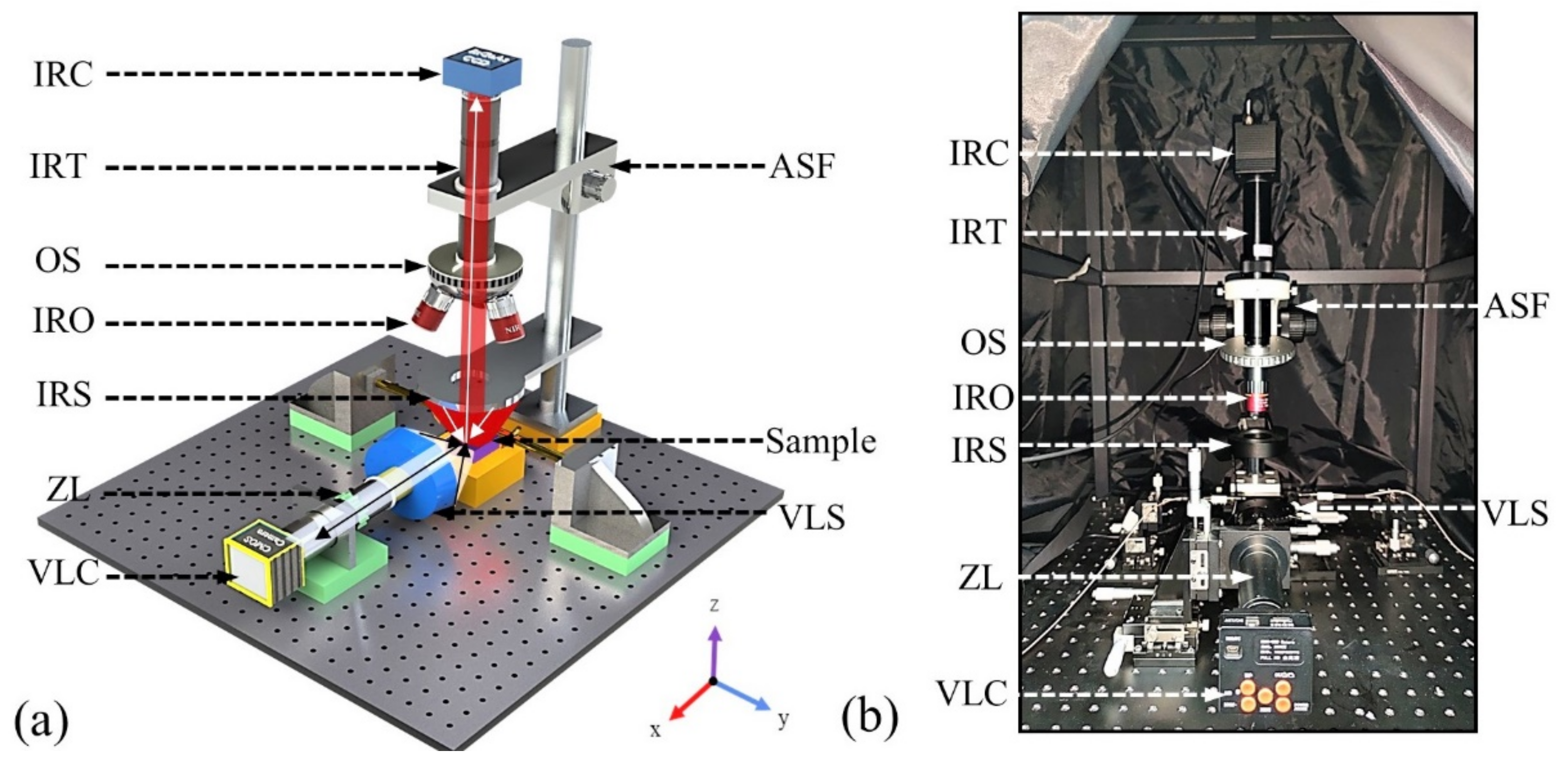
Type Ⅰ PEM system can provide the observation of a laser’s upper surface and front facet surface. The schematic of type I PEM system is shown in Figure 2a. In type I PEM system, the visible light imaging module includes a visible light CMOS camera, a zoom lens tube, and a visible light ring light source. The visible light camera has 30 million pixels, and the zoom lens can realize the adjustment of the optical magnification from 42X to 270X. In the PEM equipment system, the visible light imaging module is used to observe the laser chip surface and make the power-on probe alignment. The optical path of the visible light module is parallel to the xy plane. Infrared imaging module consists of a near-infrared InGaAs CCD camera (detection wavelength range is 900–1700 nm), infrared tube (built-in infrared anti-reflective lens and fine-tuning focus function), strut, infrared ring light source (center wavelength of light is 940 nm), objective switcher (the number of objective lenses can be assembled up to four), and infrared objectives (5X/10X/20X/50X). The light path of the infrared imaging module is perpendicular to the xy plane. When the forward or reverse bias voltages are applied to the laser, the radiated light is collected by the infrared imaging module and finally processed by the computer. The power-on module includes probe holders, tungsten steel gold-plated probes (the probe diameter can be varied from 5 to 30 μm as needed), and a DC power supply. If the laser chip has pins, it can be powered directly through the wire without the probe. The displacement module mainly includes adjustable support frame, XY displacement platform, and XYZ displacement platform. The infrared lens tube is fixed on the focusing frame. Through the focusing frame, we can realize the focusing process by adjusting the distance between the CCD and the sample. Two XY stages are placed on the bottom of the strut and the sample stage, respectively, in order to adjust the position of the observation area. Another XYZ displacement platform is placed on the bottom of the visible light imaging module to adjust the observation position and focus length. The photograph of type I PEM is shown in Figure 2b.

3.2. Type Ⅱ PEM

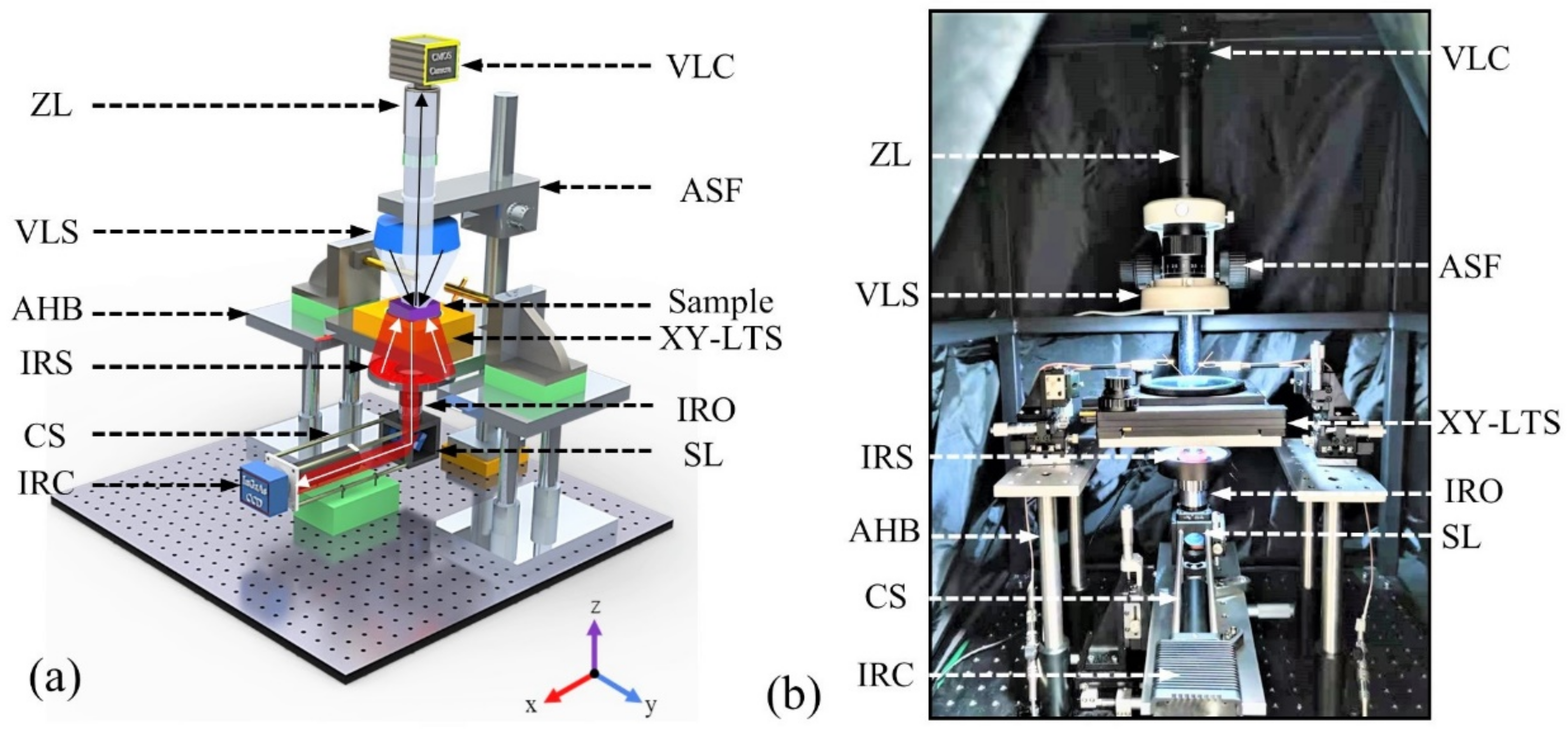
Type II PEM system can be used to observe the active region of a laser chip. The schematic of type II PEM is shown in Figure 3a. For the active region of semiconductor laser to be observed, the system structure of type II is different from type I. The first difference is that the infrared camera and the visible light are installed at the opposite position. In type II, the visible light module is installed on the adjustable support frame, and the infrared module is installed on the XYZ stage. The second is that the infrared module adopts a cage system, which can steer the light path through the infrared 90-degree steering lens, as shown in Figure 4a,b (the front surface of the lens glass is coated by broadband dielectric film to increase reflection, which can meet the reflectivity of light in the wavelength range of 1280 to 1600 nm greater than 97%, and the steering angle can be fine-tuned through the angle fine-tuning structure), and the objective is mounted on the cage plate. The third is that the XY stage in the displacement module becomes a light-transmitting stage that enables the system to observe the backside light emission while the probe is powered on the upper surface of the laser. At the same time, the probe base adds an adjustable height block for the raised sample stage. The photograph of type Ⅱ PEM is shown in Figure 3b.

4. Sample Preparation Method for Failure Analysis

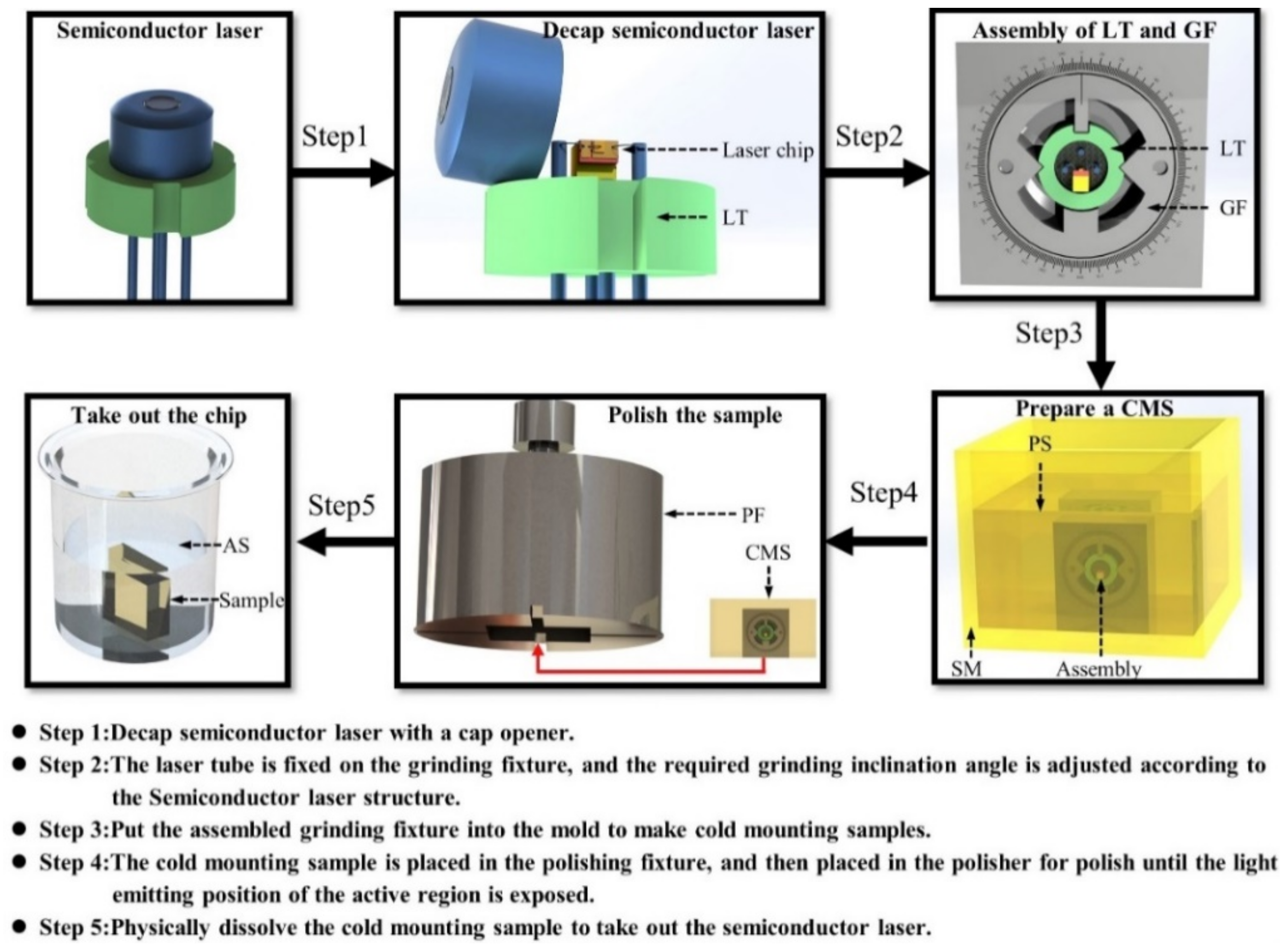
The traditional sample preparation for laser failure analysis needs to use the micro-/nano- processing. This processing method is not only expensive but also time-consuming. In this paper, we propose a simple sample preparation method of laser failure analysis that can be used in the packaged semiconductor lasers. Figure 5 shows the flow chart, and the detailed preparation steps are given as follows:
First step: Use the cap opener to decap semiconductor lasers (be careful to avoid touching the laser during the opening process). The schematic of semiconductor laser after being decapped is showed in Figure 6a.
Second step: Fix the semiconductor laser after being decapped on the grinding fixture and rotate a certain angle. As shown in the Figure 7a, the fixture is composed of an internal load block with calibration line and a shell with the tick mark. The inner load block can be rotated to a certain angle according to the tick mark. After the whole is fixed, the leads can be electrically connected to the pins and put into type I PEM system for observation from the upper surface and front facet of semiconductor lasers. After observing the intact semiconductor laser, we can further observe the active region through type II PEM system by polishing along a certain angle. As shown in Figure 6b, the angle is adjusted through the grinding fixture so that part of the bottom gold electrode of the semiconductor laser is reserved after polishing, and meanwhile the active region of the semiconductor laser can be exposed. The top view of sample after being polished is shown in Figure 6c. From the top view, we can conclude that the Au layer can be effectively used as an electrode for subsequent experiments
Third step: Put the grinding fixture into the soft silicone mold as shown in Figure 7b. Acrylic resin and butyl methacrylate were prepared according to a mass ratio of 1:0.8 to obtain a polyester solution and then were poured into the silicone mold. Place the sample at room temperature for 20 min to obtain a cold mounting sample. The maximum exposed temperature was 80 °C.
Fourth step: Embed the cold mounting sample in the polishing fixture as shown in Figure 7c and place it into the polisher for polishing. Control the polishing thickness by adjusting the micrometer head on the polishing fixture and polish it until the light-emitting position of the active region is revealed and there are some bottom gold electrodes left. The polisher material is aluminum oxide. We first use 300 grit size abrasive with 200 rpm rotation speed to polish the laser tube; then, use 600 grit size abrasive with 200 rpm rotation speed to polish the heat sink until the light-emitting position of the active region is revealed; finally, use 6000 and 12,000 grit size abrasives with 50 rpm orderly to polish laser chip for 2 min. The whole polished sample is shown in Figure 7d. The laser tube, heat sink, and gold electrode are selectively removed by tilt polishing. We can find the laser chip from the polished section, as shown in Figure 7d.
Fifth step: The sample is soaked in acetone solution for about 40 min, and then the chip can be taken out. The failure analysis sample preparation for observing the possible defect in the active region is completed, which can be put into the PEM type II system for measurement.

5. Results and Discussion

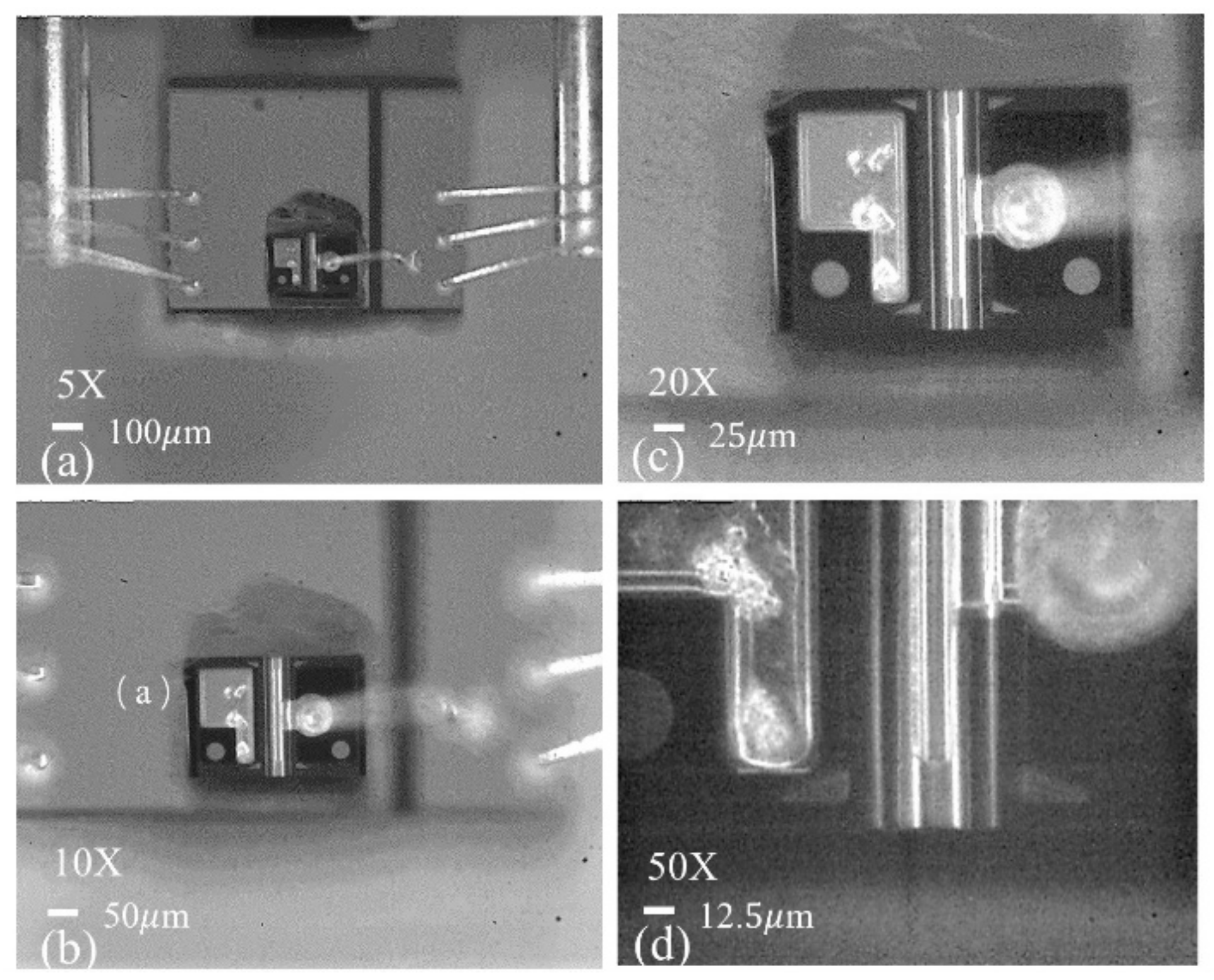
In the following experiment, we took the 1310 nm DFB TO packaged semiconductor lasers as objectives, which is provided by the corporation. The two home-made types of PEM equipment system were adopted to perform the failure analysis by detecting from the front facet and active region, respectively. As the light emission from the active region will be absorbed by the metal electrode, we employed the above sample preparation method and type II PEM system for detecting the active region. Through the type I PEM system, we took images with various magnifications (5X, 10X, 20X, and 50X) under the 940 nm light source without the bias electric source. As shown in Figure 8, the structure of semiconductor lasers was clearly observed with different magnitudes, which suggests the home-made PEM I system can realize high-definition, near-infrared imaging. When we applied 1 V positive voltage to the semiconductor laser, it was able to generate the output light. However, the emitted light spot was uneven, and there was obviously a larger discontinuity on the left side, as shown in Figure 9a. When a reverse voltage of 8 V was applied, there was a faint light spot on the left side of the front facet, as shown in Figure 9c. This was because the defect in the semiconductor laser generated the output light under the large leakage current. It needs to be noted that we needed to turn down the 940 nm illumination light source to make the light from the defect easier to be distinguished. It can be seen from the image that the discontinuous position of the forward-biased laser spot coincided with the defect light-emission position under the reverse bias voltage. Therefore, it can be preliminarily diagnosed that the semiconductor laser had leakage, and the leakage defects were concentrated in the left area of the front facet surface.
In order to further confirm the occurrence of optical radiation due to leakage current, we also detected the laser front facet surface by type I PEM system. Comparing Figure 9b with Figure 9d, we found that the emitted light under the reverse bias voltage was indeed generated through the front facet, which further proved that the laser had leakage failure.
Active region is the most important part of the semiconductor laser. Furthermore, in order to further find and ensure the defect position in the active region, we used the mentioned sample preparation method in Section 4 to deal with the semiconductor lasers. Figure 10a shows the whole semiconductor laser sample after processing. Figure 10b shows the active region was exposed after polishing, while there was some golden metal left. In order to effectively power on the sample, we positioned the two probes of the power supply module to electrode pads (labelled 1 and 2 in Figure 10a). The area of pad was larger than 200 μm× 200 μm, and the probe with the diameter of 15 μm was employed to provide electric power for the sample. The ohmic contact of the sample was changed because part of the electrode was removed. The voltage applied to the sample was larger than the initial threshold voltage of the laser so that the light emission of the active region could be observed. For this sample, we chose a forward voltage of 0.8 V as the test voltage. By applying a forward bias of 0.8 V on the pad, we were able to see the resulting electroluminescence, as is shown in Figure 10c. It was obvious that there was a large dark spot defect focused in the middle area. It can be inferred that the main reasons for the occurrence of this defect were as follows:
  • The quantum well optical power in the ridge waveguide region was relatively large. Due to the large optical power, the temperature rises resulted in defects and even local melting and polycrystalline.
  • There were trenches on both sides of the ridge waveguide. In the process of etching for forming the channel, lattice defects and surface defect states were generated. As impurities were accumulated at the channel after fabrication, defects continued to grow and climb to both sides in a large area.
  • During the operation of the semiconductor laser, there was electrostatic breakdown, which caused COD on the facet. At the same time, the defects grew and diffused from the position where COD occurred to the inside of the active region during subsequent use, and finally appeared as a larger dark area in the active region.
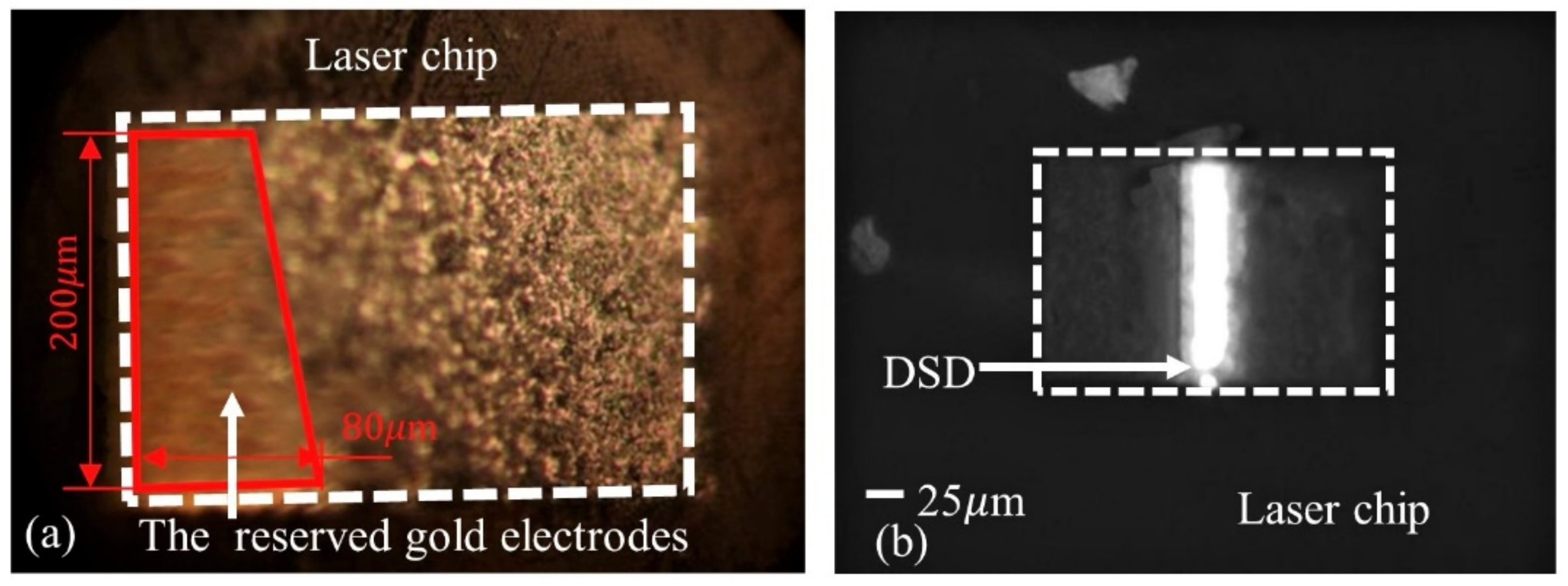
In order to further confirm the feasibility of sample preparation method and home-made PEM experimental system, we realized the back observation for another degraded semiconductor laser from the production line (the second laser sample). The whole preparation process was consistent with that shown in Figure 5. As shown in Figure 11a, part of the bottom gold electrodes of semiconductor laser was reserved after polishing. The area of reserved gold electrodes was about 100 × 80 μm, which was approximately one-third of the bottom electrode. The probe with 10 μm diameter and a forward voltage of 0.65 V was adopted. The obtained back electroluminescence image of the second laser sample through type II PEM system is shown in Figure 11b. It can be clearly observed that there were obvious DSDs in the active region of the laser. Compared with the first sample, the dark area of the second one was smaller, and the location was also different from that of the first one. Therefore, we inferred that the reasons resulting in the failure of the first and second laser samples were different, and the causes of such defects (the second laser sample) were as follows:
  • The substrate had dislocations, resulting in defects to be generated in the active area through dislocation gliding and climbing.
  • The laser internal COD occurred, which caused local melting of the crystal lattice and a huge stress. During the stress release process, dislocations were generated.
PEM has the advantages of short experiment time (0.2–0.6 h) and low cost. At the same time, non-destructive detection can be achieved for the laser whose active region is not blocked by the electrode. Due to the optical diffraction, the resolution is on the order of microns (several microns). Laser-scanning microscopy (LSM) and EBIC are two other main defect detection methods. LSM uses the focused beam as an excitation source to scan the sample in order to obtain a defect map [26,31]. Due to optical diffraction, the resolution of LSM is also at the micron level (its resolution can reach a few tenths of a micron if the sample is thin enough). However, its experiment time is longer (4 h), and the experiment cost is higher. In contrast, EBIC scans the sample with a nanometer-level electron beam to locate the defect by acquiring the distribution image of the internally induced current [32]. The resolution of EBIC is higher than that of the optical microscope (tens to hundreds of nanometers), but the difficult sample preparation (the sample thickness is required to reach a few micrometers) leads to high cost and a long period of time (0.6–1 h), and therefore it is not suitable for rapid detection [33]. When the resolution requirement is tens of nanometers, EBIC is the better solution. When the resolution requirement is around a few hundred nanometers for a laser, LSM is the better solution. When micron-level detections for lasers are performed, PEM’s rapidity and low cost have more significant advantages over other experiment solutions.

6. Conclusions

In this paper, we have presented an effective failure analysis method for semiconductor lasers with two home-made types of PEM systems and simple sample preparation. On the basis of the PEM I system, we successfully observed the light spot of defect from the upper surface and front facets under reverse bias voltage. Moreover, we further observed dark spot defects in the active region by employing the new simple sample preparation method, which does not need to involve complicated and expensive micro-/nano-processing processes. As discussed in the Results and Discussion section, PEM has the advantages of rapid detection, low cost, and non-destructive detection compared to other detection methods. The proposed failure analysis method provides an important choice for related researchers and semiconductor laser manufactures. Meanwhile, the two types of PEM systems can be important candidates for fast failure detection and analysis in the related fields including lasers and integrated circuits, among others.

Author Contributions

Conceptualization, T.S. and M.X.; methodology, T.S. and M.X.; software, T.S.; validation, T.S.; formal analysis, T.S. and M.X.; investigation, T.S. and M.X.; resources, M.X. and L.Q.; data curation, T.S.; writing—original draft preparation, T.S.; writing—review and editing, M.X.; supervision, M.X.; project administration, M.X. and L.Q.; funding acquisition, M.X. All authors have read and agreed to the published version of the manuscript.

Funding

This research was funded by ZTE Corporation Research Foundation (grant number HC-CN-20200304002), National Natural Science Foundation of China (grant number 61905217), Open Project Program of Wuhan National Laboratory for Optoelectronics (grant number 2019WNLOKF012), and Natural Science Foundation of Zhejiang Province (grant number LQ19F040010).

Data Availability Statement

Data are available from the authors on request.

Conflicts of Interest

The authors declare no conflict of interest.

References

  1. Hall, R.N.; Fenner, G.E.; Kingsley, J.D.; Soltys, T.J.; Carlson, R.O. Coherent light emission from GaAs junctions. Phys. Rev. Lett. 1962, 9, 366. [Google Scholar] [CrossRef]
  2. Kao, K.C.; Hockham, G.A. Dielectric-fibre surface waveguides for optical frequencies. Proc. Inst. Elec. Eng. 1966, 113, 1151–1158. [Google Scholar] [CrossRef] [Green Version]
  3. Cranch, G.A.; Flockhart, G.M.; Kirkendall, C.K. Distributed Feedback Fiber Laser Strain Sensors. IEEE Sen. J. 2008, 8, 1161–1172. [Google Scholar] [CrossRef]
  4. Chen, X.F.; Dong, X.; Lv, H.J.; Hu, Y.X.; Yu, X.J.X.; Chen, F.; Liu, S.C. Real-time interrogation technology for a large-scale fiber-ring laser sensor array. IEEE Photon. J. 2017, 9, 1–9. [Google Scholar] [CrossRef]
  5. Rabi, L.; André, S.; Oliver, M.; Stefan, K.; Ludger, O. Investigations on laser welding of dissimilar joints of steel and aluminum using a high-power diode laser. J. Laser Appl. 2018, 30, 032422. [Google Scholar]
  6. Paul, M. Review of ladar: A historic, yet emerging, sensor technology with rich phenomenology. Opt. Eng. 2012, 51, 060901. [Google Scholar]
  7. Chapuran, T.E.; Toliver, P.; Peters, N.A.; Jackel, J.; Goodman, M.S.; Runser, R.J.; McNown, S.R.; Dallmann, N.; Hughes, R.J.; McCabe, K.P.; et al. Optical networking for quantum key distribution and quantum communications. New J. Phys. 2009, 11, 105001. [Google Scholar] [CrossRef]
  8. Gourley, P.L. Microstructured semiconductor lasers for high-speed information processing. Nature 1994, 371, 571–577. [Google Scholar] [CrossRef]
  9. Eaton, S.W.; Fu, A.; Wong, A.B.; Ning, C.Z.; Yang, P.D. Semiconductor nanowire lasers. Nat. Rev. Mater. 2016, 1, 16028. [Google Scholar] [CrossRef]
  10. Nakamura, S. The Roles of Structural Imperfections in InGaN-Based Blue Light-Emitting Diodes and Laser Diodes. Science 1998, 281, 956–961. [Google Scholar] [CrossRef] [Green Version]
  11. Jung, D.; Herrick, R.; Norman, J.; Turnlund, K.; Jan, C.; Feng, K.Y.; Gossard, A.C.; Bowers, J.E. Impact of threading dislocation density on the lifetime of InAs quantum dot lasers on Si. Appl. Phys. Lett. 2018, 112, 153507. [Google Scholar] [CrossRef]
  12. Gontijo, I.; Qiu, Y.M.; Shapiro, A.A. Reliability of semiconductor laser packaging in space applications. In Proceedings of the 2008 2nd Electronics System-Integration Technology Conference, Greenwich, UK, 1–4 September 2008; pp. 1127–1130. [Google Scholar]
  13. Field, E.S.; Kletecka, D.E. Impact of contamination and aging effects on the long-term laser damage resistance of SiO2/HfO2/TiO2 high reflection coatings for 1054 nm. Opt. Eng. 2019, 58, 105105. [Google Scholar] [CrossRef] [Green Version]
  14. Magistrali, F.; Sala, D.; Salmini, G.; Vanzi, M.; Fantini, F.; Giansante, M.; Zazzetti, L. ESD induced degradation mechanisms of InGaAsP/InP lasers. Qual. Reliab. Eng. Int. 1992, 8, 287–293. [Google Scholar] [CrossRef]
  15. Yuasa, T.; Ogawa, M.; Endo, K.; Yonezu, H. Degradation of (AlGa)As DH lasers due to facet oxidation. Appl. Phys. Lett. 1978, 32, 119. [Google Scholar] [CrossRef]
  16. Schoedl, T.; Schwarz, U.T. Facet degradation of GaN heterostructure laser diodes. Appl. Phys. Lett. 2005, 97, 123102. [Google Scholar] [CrossRef]
  17. Waters, R.G. Diode laser degradation mechanisms: A review. Prog. Quantum Electron. 1991, 15, 153–174. [Google Scholar] [CrossRef]
  18. Jiménez, J. Laser diode reliability: Crystal defects and degradation modes. C. R. Phys. 2003, 4, 663–673. [Google Scholar] [CrossRef]
  19. Sanayeh, M.B.; Jaeger, A.; Schmid, W.; Tautz, S.; Brick, P.; Streubel, K. Investigation of dark line defects induced by catastrophic optical damage in broad-area AlGaInP laser diodes. Appl. Phys. Lett. 2006, 89, 101111. [Google Scholar] [CrossRef]
  20. Ueda, O.; Yamakoshi, S.; Komiya, S.; Akita, K.; Yamaoka, Y. Transmission electron microscope observation of dark-spot defects in InGaAsP/InP double-heterostructure light-emitting diodes aged at high temperature. Appl. Phys. Lett. 1980, 36, 300–301. [Google Scholar] [CrossRef]
  21. Nomoto, E.; Nakahara, K.; Shimaoka, M. Stress on junction-down-mounted ridge-waveguide laser diodes. Jpn. J. Appl. Phys. 2005, 44, 1756–1758. [Google Scholar] [CrossRef]
  22. Dagdostar, S.; Souto, J.; Jiménez, J. CL as a tool for device characterisation: The case of laser diode degradation. Nano Ex. 2021, 2, 014001. [Google Scholar] [CrossRef]
  23. Liu, J.X.; Wang, J.; Sun, X.J.; Sun, Q.; Feng, M.X.; Ge, X.T.; Ning, J.Q.; Zhou, R.; Zhou, Y.; Gao, H.W.; et al. Performance improvement of InGaN-based laser grown on Si by suppressing point defects. Opt. Express 2019, 27, 25943–25952. [Google Scholar] [CrossRef] [PubMed]
  24. Yellen, S.L.; Shepard, A.H.; Dalby, R.J.; Baumann, J.A.; Serreze, H.B.; Guido, T.S.; Soltz, R.; Bystrom, K.J.; Harding, C.M.; Waters, R.G. Reliability of GaAs-Based Semiconductor Diode Lasers: 0.6–1.1 μm. IEEE J. Quantum Electron. 1993, 29, 2058–2067. [Google Scholar] [CrossRef]
  25. Ueda, O.; Imai, H.; Yamaguchi, A.; Komiya, S.; Umebu, I.; Kotani, T. Mechanism of catastrophic degradation in 1.3-μm V-grooved substrate buried-heterostructure lasers with the application of large pulsed currents. J. Appl. Phys. 1984, 55, 665. [Google Scholar] [CrossRef]
  26. Lei, C.; Li, N.; Xie, C.; Carson, R.; Sun, X.Y.; Luo, W.L.; Zhao, L.; Helms, C.; Jensen, D.; Liu, C. Emcore VCSEL failure mechanism and resolution. In Proceedings of the SPIE, Vertical-Cavity Surface-Emitting Lasers XIV, San Francisco, CA, USA, 5 February 2010; p. 761504. [Google Scholar]
  27. Park, K.H.; Lee, J.K.; Jang, D.H.; Cho, H.S.; Park, C.S.; Pyun, K.E. Characterization of catastrophic optical damage in Al-free InGaAs/InGaP 0.98 μm high-power lasers. Appl. Phys. Lett. 1998, 73, 2576. [Google Scholar] [CrossRef]
  28. McEifresh, D.K.; Lopez, L.D.; Vacar, D. Reverse-bias emission sheds light on the failure mechanism of degraded vertical-cavity surface-emitting lasers. J. Appl. Phys. 2006, 99, 123113. [Google Scholar] [CrossRef]
  29. Richard, J.R. Microelectrionics Failure Analysis, 6th ed.; ASM International: Materials Park, OH, USA, 2011; pp. 279–281. [Google Scholar]
  30. Yang, S.C.; Pang, L.; Wang, C.P.; Huang, S.B.; Chen, C.L.; Chiang, P.F.; Lee, A.T.; Chu, M.T. Failure and degradation mechanisms of high-power white light emitting diodes. Microelectron. Reliab. 2010, 50, 959–964. [Google Scholar] [CrossRef]
  31. Bushmaker, A.W.; Lingley, Z.; Brodie, M.; Foran, B.; Sin, Y. Optical Beam Induced Current and Time Resolved Electro-Luminescence in Vertical Cavity Surface Emitting Lasers During Accelerated Aging. IEEE Photonics J. 2019, 11, 1–11. [Google Scholar] [CrossRef]
  32. Mann, R.S.; McElfresh, D.K. Categorizing light output degradation failures in LEDs using the relationship between defect revealing mechanisms responsible for electroluminescence (EL), cathodoluminescence (CL), EBIC, and reverse bias photoemission (RP). In Proceedings of the 1995 IEEE International Reliability Physics Symposium, Las Vegas, NV, USA, 4 April 1995; pp. 177–186. [Google Scholar]
  33. Ueda, O.; Herrick, R.W. Failure Analysis of Semiconductor Optical Devices. In Book Materials and Reliability Handbook for Semiconductor Optical and Electron Devices; Ueda, O., Pearton, S.J., Eds.; Springer: New York, NY, USA, 2013; p. 22. [Google Scholar]
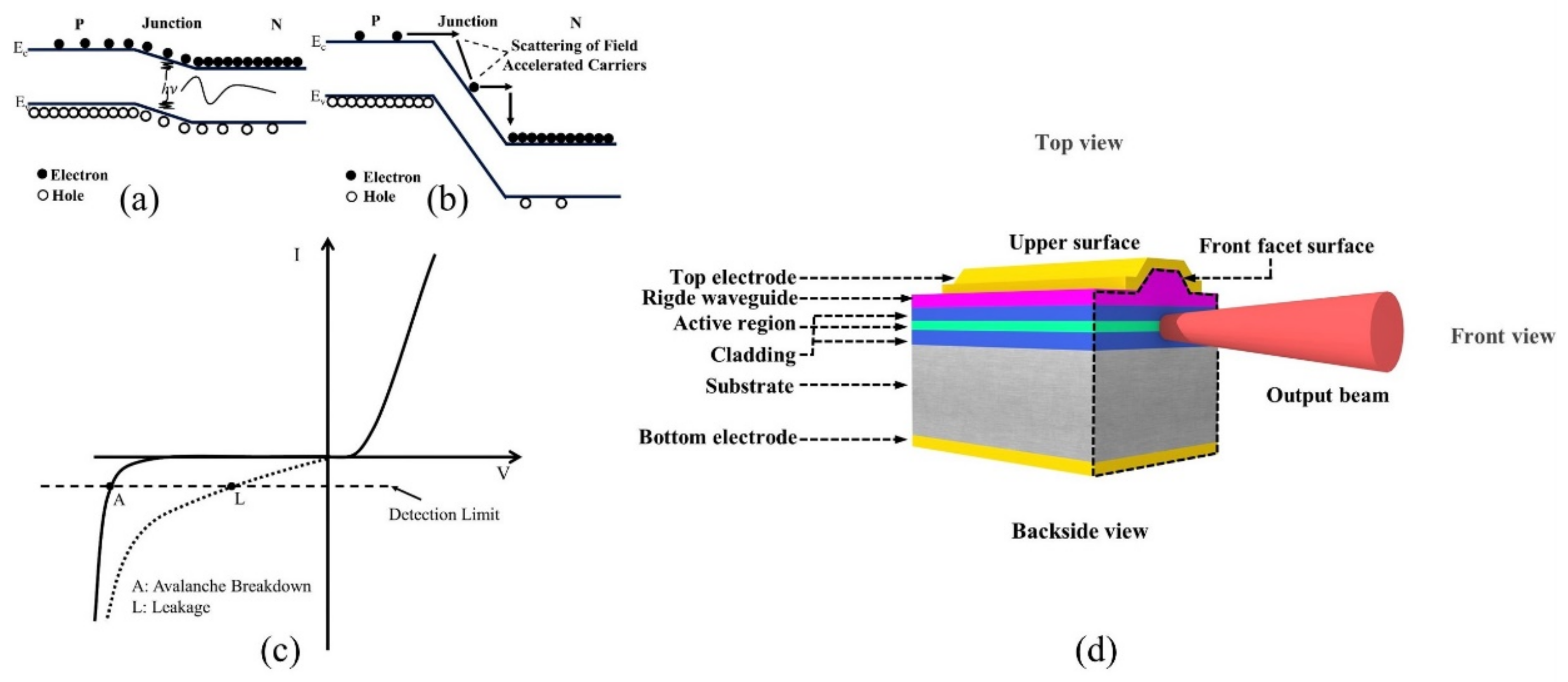
Figure 1. (a) Radiative recombination in forward biased junction; (b) relaxation accompanied with light emission in reverse biased junction; (c) I-V curve of PN-junction and PEM detection under reverse bias [29]; (d) schematic of laser structure and observation direction.
Photonics 08 00184 g001
Figure 2. (a) Schematic of type Ⅰ PEM; (b) photograph of type Ⅰ PEM. IRC, infrared camera; IRT, infrared tube; OS, objective switcher; IRO, infrared objectives; IRS, infrared source; ZL, zoom lens tube; VLC, visible light camera; ASF, adjustable support frame; VLS, visible light source. Infrared light propagates along the direction of the white arrow in the red-colored area. Visible light propagates along the direction of the black arrow in the white-colored area.
Photonics 08 00184 g002
Figure 3. (a) Schematic of type Ⅱ PEM; (b) photograph of type Ⅱ PEM. AHB, adjustable height block; CS, cage system; XY-LTS, XY light transmitting displacement stage; SL, steering lens. Infrared light propagates along the direction of the white arrow in the red-colored area. Visible light propagates along the direction of the black arrow in the white-colored area.
Photonics 08 00184 g003
Figure 4. (a) Schematic of 90-degree steering lens; (b) schematic of optical path in 90-degree steering lens (the input light can be steered by SL to make the output light perpendicular to the incident light). AFTS, angle fine-tuning structure.
Photonics 08 00184 g004
Figure 5. Sample preparation flow chart. LT, laser tube; GF, grinding fixture; PS, polyester solution; SM, silicone mold; CMS, cold mounting sample; PF, polishing fixture; AS, acetone solution.
Photonics 08 00184 g005
Figure 6. (a) The schematic of semiconductor laser after being decapped; (b) the front view of sample after being polished; (c) the top view of sample after being polished. The area enclosed by the dashed line is the polished area. Under the condition that the laser is effectively powered, the light-transmitting window of the substrate is made by polishing.
Photonics 08 00184 g006
Figure 7. (a) The schematic of the assembly of laser tube and grinding fixture; (b) silicone mold; (c) polishing fixture; (d) the cold mounting sample after polishing. After polishing, the laser chip can be found from the polished section.
Photonics 08 00184 g007
Figure 8. Infrared imaging of semiconductor laser under different magnifications in PEM Ⅰ system: (a) 5X; (b) 10X; (c) 20X; (d) 50X.
Photonics 08 00184 g008
Figure 9. (a) Image obtained from upper surface of semiconductor laser under 1 V forward bias voltage; (b) image obtained from the front facet of semiconductor laser without bias voltage; (c) image obtained from the upper surface of semiconductor laser under 8 V reverse bias voltage; (d) image obtained from the front facet of semiconductor laser under 8 V reverse bias voltage.
Photonics 08 00184 g009
Figure 10. (a) The upper surface of polished semiconductor laser; (b) backside view of polished semiconductor laser; (c) dark spot defects observation through electroluminescence imaging. The position of the laser chip is marked by a dotted line. The area enclosed by the solid yellow line is the residual heat sink. The dark spot in the active region is observed in Figure 10c.
Photonics 08 00184 g010
Figure 11. (a) Backside view of the second polished semiconductor laser; (b) dark spot defect observation through electroluminescence imaging (the second laser sample). The position of the laser chip is marked by a dotted line. Approximately one-third of the bottom electrode of the second semiconductor sample is reserved to ensure effective power supply for the test in Figure 11a. The DSD in the active region is observed in Figure 11b.
Photonics 08 00184 g011
Publisher’s Note: MDPI stays neutral with regard to jurisdictional claims in published maps and institutional affiliations.